EP0287444A1 - Vorrichtung zur optischen Steuerung einer Abtastantenne - Google Patents
Vorrichtung zur optischen Steuerung einer Abtastantenne Download PDFInfo
- Publication number
- EP0287444A1 EP0287444A1 EP88400856A EP88400856A EP0287444A1 EP 0287444 A1 EP0287444 A1 EP 0287444A1 EP 88400856 A EP88400856 A EP 88400856A EP 88400856 A EP88400856 A EP 88400856A EP 0287444 A1 EP0287444 A1 EP 0287444A1
- Authority
- EP
- European Patent Office
- Prior art keywords
- modulators
- control device
- beams
- modulator
- optical
- Prior art date
- Legal status (The legal status is an assumption and is not a legal conclusion. Google has not performed a legal analysis and makes no representation as to the accuracy of the status listed.)
- Granted
Links
- 230000003287 optical effect Effects 0.000 title claims abstract description 32
- 230000005540 biological transmission Effects 0.000 claims description 12
- 239000004065 semiconductor Substances 0.000 claims description 6
- 239000004973 liquid crystal related substance Substances 0.000 claims description 4
- 230000000694 effects Effects 0.000 claims description 3
- 238000002310 reflectometry Methods 0.000 claims description 3
- 239000000463 material Substances 0.000 claims description 2
- 239000013307 optical fiber Substances 0.000 claims description 2
- 210000002858 crystal cell Anatomy 0.000 claims 1
- 230000010363 phase shift Effects 0.000 abstract description 11
- 238000010586 diagram Methods 0.000 description 3
- 239000000835 fiber Substances 0.000 description 3
- 239000011159 matrix material Substances 0.000 description 3
- 230000005855 radiation Effects 0.000 description 3
- 238000010009 beating Methods 0.000 description 2
- 238000001514 detection method Methods 0.000 description 2
- 238000000034 method Methods 0.000 description 2
- 230000000704 physical effect Effects 0.000 description 2
- 229910003327 LiNbO3 Inorganic materials 0.000 description 1
- 239000004988 Nematic liquid crystal Substances 0.000 description 1
- 239000004990 Smectic liquid crystal Substances 0.000 description 1
- 238000010521 absorption reaction Methods 0.000 description 1
- 238000003491 array Methods 0.000 description 1
- 230000001934 delay Effects 0.000 description 1
- 238000009792 diffusion process Methods 0.000 description 1
- 230000001939 inductive effect Effects 0.000 description 1
- 239000012528 membrane Substances 0.000 description 1
- 238000013139 quantization Methods 0.000 description 1
- 238000005070 sampling Methods 0.000 description 1
- 239000000758 substrate Substances 0.000 description 1
Images

Classifications
-
- G—PHYSICS
- G02—OPTICS
- G02F—OPTICAL DEVICES OR ARRANGEMENTS FOR THE CONTROL OF LIGHT BY MODIFICATION OF THE OPTICAL PROPERTIES OF THE MEDIA OF THE ELEMENTS INVOLVED THEREIN; NON-LINEAR OPTICS; FREQUENCY-CHANGING OF LIGHT; OPTICAL LOGIC ELEMENTS; OPTICAL ANALOGUE/DIGITAL CONVERTERS
- G02F2/00—Demodulating light; Transferring the modulation of modulated light; Frequency-changing of light
- G02F2/002—Demodulating light; Transferring the modulation of modulated light; Frequency-changing of light using optical mixing
-
- H—ELECTRICITY
- H01—ELECTRIC ELEMENTS
- H01Q—ANTENNAS, i.e. RADIO AERIALS
- H01Q3/00—Arrangements for changing or varying the orientation or the shape of the directional pattern of the waves radiated from an antenna or antenna system
- H01Q3/26—Arrangements for changing or varying the orientation or the shape of the directional pattern of the waves radiated from an antenna or antenna system varying the relative phase or relative amplitude of energisation between two or more active radiating elements; varying the distribution of energy across a radiating aperture
- H01Q3/2676—Optically controlled phased array
Definitions
- the invention relates to a device for the optical control of a scanning antenna and more particularly to a device making it possible to control by its optical means the radiation pattern of a radar antenna emitting for example in the frequency band 1 - 12 GHz.
- the proposed device provides in particular the angular scanning function of the radar beam from the phase control of each element of the antenna.
- the invention is applicable to antennas with electronic scanning, each radiating element of which is electronically controlled independently so as to obtain scanning for the antenna.
- Electronic scanning changes the position of the scanning beam. Beam scanning should be done quickly compared to the radar repetition time.
- the electronic control according to a method known in the art, consists in acting on the respective phases of the controls of the various radiating elements. It is therefore advisable to carry out a rapid phase control.
- a microwave phase shifter is associated with each antenna element.
- the invention relates to a device for optical control of the antenna elements making it possible to avoid the use of these microwave phase shifters.
- the invention therefore relates to a device for optical control of a scanning antenna comprising an array of antenna elements, the various elements being arranged in a determined order and each controlled by a microwave generator, characterized in that it comprises also: - a light source simultaneously emitting at least two collinear beams of different frequencies; optical transmission means determining as many optical paths as there are microwave generators, arranged in the same determined order as that of the antenna elements, each optical path having an input receiving the two beams emitted by the laser source and retransmitting it to an output, and each optical path of determined rank (2 for example) having a length greater than that of the optical path of lower rank according to the example taken; - a set of photodetectors, each photodetector being optically coupled to an output of an optical path, detecting the light intensity coming from this output and supplying a microwave generator with an intensity control signal whose frequency reflects the beat due to two frequencies of the two beams emitted by the laser source.
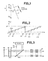
- FIG. 1 represents a linear network of elements E1 to EN of antennas, the main emission lobe of which is directed in a direction such that the radiated wave plane makes an angle ⁇ with the plane of the antenna array.
- ⁇ wavelength emitted
- ⁇ angle made by the radiated wave plane with the plane of the array of antenna elements
- ⁇ length of part of the antenna array for which a phase shift of 2 ⁇ radians is obtained.
- the emission of the beam around a direction will be obtained by limiting the phase excursion to the interval 0-2 ⁇ and by controlling each elementary antenna by increments of amplitude 2 ⁇ / N, N being the number of quantization levels of the phase law.
- N being the number of quantization levels of the phase law.
- a phase control law is obtained in which the control of each element is phase-shifted by 2 ⁇ / N relative to the neighboring elements. It is the same for another series of elements E ⁇ 1 to E ⁇ N.
- microwave phase shifter networks are bulky, expensive and require a high consumption of electric current.
- the invention relates to a phase control device with optical beams making it possible to avoid the drawbacks of known systems.
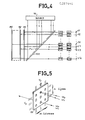
- FIG. 3 represents an exemplary embodiment of the device according to the invention.
- Each spatial modulator consists of n ⁇ n cells whose reflectivity can be controlled by means of voltages V ⁇ V y applied to row and column electrodes; - a semi-reflecting mirror MS1 makes it possible to reflect the two beams emitted by the laser source towards the modulators; a network of n ⁇ n photodetectors receiving, by means of the semi-reflecting mirror MS, the optical signals at frequencies ⁇ 0, ⁇ 1 having undergone the phase shifts ⁇ o and ⁇ l respectively such that:
- c represents the speed of light
- d represents the distance between two modulators
- N the number of modulators.
- n ⁇ n microwave generators controlled by the signal from each photodetector.
- the phase of the beat signal between the two beams at frequency ⁇ 0 and ⁇ 1 will serve as a pilot for the relative phases between the n ⁇ n elements of the antenna.
- each modulator M1 to MN reflects part of the beams received from the source SL towards a photodetector P1 to PN, while it lets pass to the modulator according to the rest of the beams.
- the modulator M1 reflects part of the beams and transmits the rest of the light to the modulators M2 to MN.
- the photodetectors P1 to PN receive light beams having undergone more or less significant phase shifts due to the distance traveled by the light beams according to the modulator which reflected the light.
- the photocurrent detected iph resulting from this wave beat is proportional to the square of ⁇ iph ⁇ ⁇ ⁇ ⁇ 2
- the iph photocurrent is therefore proportional to: iph ⁇ l + cos [ ⁇ .t - ⁇ . z vs ]
- FIG. 5 An exemplary embodiment of a spatial modulator has been shown in FIG. 5. It comprises a matrix of elements controlled by row and column electrodes. In this matrix with n rows and m columns, a single crossing point is controlled to reflect the light. The other crossing points are ordered to transmit it.
- the spatial modulator therefore provides controlled reflection of the incident wave at a single point of coordinates XY under the action of applied voltages V X and V Y.
- the number of points m ⁇ n corresponds to the number of elements of the antenna, ie: in the case where the distance between elements is of the order of 0.6 ⁇ : S: antenna surface ⁇ : emission wavelength.
- the physical effects that can be used to perform such a function are as follows: - variation of index in liquid crystals leading to a variation of reflectivity of the liquid crystal substrate interface ( ⁇ n ⁇ 0.2). - electro-reflectance in semiconductor materials and in particular in quantum multi-well structures.
- all the space modulators M1, M2 to MN are lit simultaneously by transmission from semi-transparent plates MT1, MT2, ... MTN and from a single laser source emitting on the two frequencies ⁇ 0 and ⁇ 1 .
- the semi-transparent plates are parallel aligned in the direction of the beams emitted by the source SL.
- Each modulation M1 to MN is associated with a semi-transparent plate MT 1 to MTN.
- the spatial modulator operates by local variation of transmission, controlled under the action of applied voltages V X and V Y.
- V X and V Y A number of these devices exist from the following effects: - birefringence induced in nematic liquid crystals addressed by TFT, - controlled diffusion in smectic liquid crystals, - local membrane deformation, - birefringence induced by magneto-optical effect.
- Each space modulator M1 to MN is associated with another semi-transparent mirror MU1 to MUN located on the other side of the space modulator with respect to the semi-transparent mirrors MT1 to MTN.
- the semi-transparent mirrors MU1 to MUN are parallel and aligned in the same direction so as to return the light towards the photodetectors P1 to PN whose outputs are connected to the microwave generators G1 to GN not shown.
- modulators M1 to MN The control of modulators M1 to MN is such that each modulator transmits part of the light beams, emitted by the source, to a single photodetector.
- the photodetectors P1 to PN receive light beams having traveled different paths, the length of the paths increasing with the sequence numbers 1 to N of the photodetectors P1 to PN.
- the path differences and therefore the respective positions of the modulators are provided to obtain, between two neighboring modulators, a phase shift of 2 ⁇ / N or a phase shift of 2 ⁇ between the modulator M1 and the modulator MN.
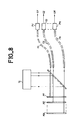
- the system of FIG. 6 is also applicable by using modulators operating in reflection.
- the modulators M1, M2, ... MN are aligned in the same plane in the same direction.
- the light source SL emits the two collinear light beams of frequencies ⁇ 0 and ⁇ 1 to a semi-reflecting MW mirror. This retransmits the two beams in a direction parallel to the alignment direction of the modulators M1 to MN.
- Each modulator M1 to MN is associated with a semi-reflecting mirror MV1 to MVN.
- the mirrors MV1 to MVN are aligned in the direction of the beams and each of them reflects part of the light beams towards the associated modulator.
- Each modulator is controlled so that only one of these zones (or part of its surface) reflects part of the beams towards the associated mirror.
- the associated mirror reflects this part of the beam towards a photodetector P1, ... PN, through the semi-reflecting mirror MW.
- the modulator M1 reflects a part of the frequency beams 0 towards the photodetector P1 and the modulator MN reflects another part towards the photodetector PN.
- the two waves ⁇ 0 and ⁇ 1 are easily generated from an acousto-optical cell controlled by a microwave signal.
- ⁇ ⁇ ⁇ 1 - ⁇ 0.
- Ultrasonic absorption limits the use of these cells for higher frequencies (4 to 12 GHz).
- the desired frequency difference can be obtained by: - association of Bragg cells, - beating between two modes of the same laser cavity (gas laser; semiconductor laser), - beat between two independent monofrequency lasers with a frequency difference equal to ⁇ ⁇ (Semiconductor lasers).
- An interesting improvement to the device consists in using a network of n2 single-mode optical fibers of the same length for the transmission of the signal to the network of photodetectors. These fibers make the emission part of the antenna independent of the optical processor ensuring the control of phase shifts.
- n2 3 S ⁇ ⁇ 2
- the spatial modulators will each be in the form of a matrix of points with a number of points equal to 100 ⁇ 100.
- the dimension of each point could be 30 ⁇ 30 ⁇ m.
- the antenna scanning control device thus described has the following advantages: - Control of the phase of the microwave signal by programmable optical delays on space modulators. The device therefore avoids the use of microwave phase shifters and their power systems. - Space modulators lit by the laser source can be replaced by two-dimensional arrays of semiconductor lasers. - It is possible to vary the frequencies ⁇ o and ⁇ l of the incident beam (frequency agility).
Landscapes
- Physics & Mathematics (AREA)
- General Physics & Mathematics (AREA)
- Nonlinear Science (AREA)
- Optics & Photonics (AREA)
- Variable-Direction Aerials And Aerial Arrays (AREA)
Applications Claiming Priority (2)
| Application Number | Priority Date | Filing Date | Title |
|---|---|---|---|
| FR8705267A FR2614136B1 (fr) | 1987-04-14 | 1987-04-14 | Dispositif de commande optique d'une antenne a balayage |
| FR8705267 | 1987-04-14 |
Publications (2)
| Publication Number | Publication Date |
|---|---|
| EP0287444A1 true EP0287444A1 (de) | 1988-10-19 |
| EP0287444B1 EP0287444B1 (de) | 1992-06-17 |
Family
ID=9350094
Family Applications (1)
| Application Number | Title | Priority Date | Filing Date |
|---|---|---|---|
| EP88400856A Expired - Lifetime EP0287444B1 (de) | 1987-04-14 | 1988-04-08 | Vorrichtung zur optischen Steuerung einer Abtastantenne |
Country Status (5)
| Country | Link |
|---|---|
| US (1) | US4864312A (de) |
| EP (1) | EP0287444B1 (de) |
| JP (1) | JP2754488B2 (de) |
| DE (1) | DE3872032T2 (de) |
| FR (1) | FR2614136B1 (de) |
Cited By (3)
| Publication number | Priority date | Publication date | Assignee | Title |
|---|---|---|---|---|
| EP0442562A1 (de) * | 1990-02-16 | 1991-08-21 | Hollandse Signaalapparaten B.V. | Antennensystem mit verstellbarer Strahlbreite und Strahlrichtung |
| WO1991014196A1 (fr) * | 1990-03-16 | 1991-09-19 | Thomson-Csf | Dispositif de creation de retards optiques et application a un systeme de commande optique d'une antenne a balayage |
| CN112350073A (zh) * | 2020-09-29 | 2021-02-09 | 北京理工大学 | 一种基于次镜阵列的超大口径反射天线 |
Families Citing this family (15)
| Publication number | Priority date | Publication date | Assignee | Title |
|---|---|---|---|---|
| DE3769301D1 (de) * | 1986-12-03 | 1991-05-16 | Philips Nv | Magnetkopf mit einem elektro-chemisch inerten spalt aus hartem material. |
| FR2674391B1 (fr) * | 1991-03-19 | 1993-06-04 | Thomson Csf | Dispositif d'intercorrelation large bande et dispositif mettant en óoeuvre ce procede. |
| US5103495A (en) * | 1991-04-11 | 1992-04-07 | The United States Of America As Represented By The Secretary Of The Air Force | Partitioned optical delay line architecture for time steering of large 1-D array antennas |
| FR2681988A1 (fr) * | 1991-09-27 | 1993-04-02 | Thomson Csf | Laser de puissance a deflexion. |
| US5365239A (en) * | 1991-11-06 | 1994-11-15 | The United States Of America As Represented By The Secretary Of The Navy | Fiber optic feed and phased array antenna |
| US5191339A (en) * | 1992-03-05 | 1993-03-02 | General Electric Company | Phased-array antenna controller |
| US5187487A (en) * | 1992-03-05 | 1993-02-16 | General Electric Company | Compact wide tunable bandwidth phased array antenna controller |
| US5461687A (en) * | 1992-03-18 | 1995-10-24 | Trw Inc. | Wavelength controlled optical true time delay generator |
| WO1996026554A1 (fr) * | 1995-02-24 | 1996-08-29 | Thomson-Csf | Dephaseur hyperfrequence et application a une antenne reseaux |
| FR2755516B1 (fr) | 1996-11-05 | 1999-01-22 | Thomson Csf | Dispositif compact d'illumination |
| US6243012B1 (en) | 1996-12-31 | 2001-06-05 | Lucent Technologies Inc. | Inexpensive modulated backscatter reflector |
| FR2819061B1 (fr) * | 2000-12-28 | 2003-04-11 | Thomson Csf | Dispositif de controle de polarisation dans une liaison optique |
| WO2010001438A1 (ja) * | 2008-07-03 | 2010-01-07 | 独立行政法人情報通信研究機構 | ファイバ無線用ユニット及びファイバ無線用システム |
| EP2244102A1 (de) * | 2009-04-21 | 2010-10-27 | Astrium Limited | Radarsystem |
| US12519218B2 (en) | 2021-03-30 | 2026-01-06 | Nec Corporation | Liquid crystal antenna and method for manufacturing liquid crystal antenna |
Citations (2)
| Publication number | Priority date | Publication date | Assignee | Title |
|---|---|---|---|---|
| US3878520A (en) * | 1973-01-24 | 1975-04-15 | Stanford Research Inst | Optically operated microwave phased-array antenna system |
| US4238797A (en) * | 1979-05-25 | 1980-12-09 | The United States Of America As Represented By The Secretary Of The Army | Multi-beam antenna controller |
Family Cites Families (5)
| Publication number | Priority date | Publication date | Assignee | Title |
|---|---|---|---|---|
| US4028702A (en) * | 1975-07-21 | 1977-06-07 | International Telephone And Telegraph Corporation | Fiber optic phased array antenna system for RF transmission |
| NL7807170A (nl) * | 1978-06-30 | 1980-01-03 | Hollandse Signaalapparaten Bv | Radarsysteem. |
| US4241351A (en) * | 1979-05-11 | 1980-12-23 | The United States Of America As Represented By The Secretary Of The Army | Array antenna controller |
| US4583096A (en) * | 1983-05-23 | 1986-04-15 | The United States Of America As Represented By The Secretary Of The Air Force | Fiber optic data distribution for phased array antenna |
| US4739334A (en) * | 1986-09-30 | 1988-04-19 | The United States Of America As Represented By The Secretary Of The Air Force | Electro-optical beamforming network for phased array antennas |
-
1987
- 1987-04-14 FR FR8705267A patent/FR2614136B1/fr not_active Expired
-
1988
- 1988-04-08 EP EP88400856A patent/EP0287444B1/de not_active Expired - Lifetime
- 1988-04-08 DE DE8888400856T patent/DE3872032T2/de not_active Expired - Fee Related
- 1988-04-11 US US07/180,313 patent/US4864312A/en not_active Expired - Lifetime
- 1988-04-14 JP JP63092630A patent/JP2754488B2/ja not_active Expired - Fee Related
Patent Citations (2)
| Publication number | Priority date | Publication date | Assignee | Title |
|---|---|---|---|---|
| US3878520A (en) * | 1973-01-24 | 1975-04-15 | Stanford Research Inst | Optically operated microwave phased-array antenna system |
| US4238797A (en) * | 1979-05-25 | 1980-12-09 | The United States Of America As Represented By The Secretary Of The Army | Multi-beam antenna controller |
Non-Patent Citations (3)
| Title |
|---|
| JOURNAL OF LIGHTWAVE TECHNOLOGY, vol. LT-3, no. 5, octobre 1985, pages 992-998, New York, US; R.A. SOREF: "Voltage-controlled optical/RF phase shifter" * |
| JOURNAL OF OPTICS, vol. 15, no. 6, novembre/décembre 1984, pages 403-407, Paris, FR; J.P. GOEDGEBUER et al.: "Nouvelle technique de modulation électro-optique adaptée aux sources à spectre large" * |
| RADAR-82, INTERNATIONAL CONFERENCE, 18-20 octobre 1982, pages 408-412, Londres, GB; J.R. FORREST et al.: "Optical fibre networks for signal distribution and control in phased array radars" * |
Cited By (7)
| Publication number | Priority date | Publication date | Assignee | Title |
|---|---|---|---|---|
| EP0442562A1 (de) * | 1990-02-16 | 1991-08-21 | Hollandse Signaalapparaten B.V. | Antennensystem mit verstellbarer Strahlbreite und Strahlrichtung |
| TR24873A (tr) * | 1990-02-16 | 1992-07-01 | Hollandse Signaalapparaten Bv | AYARLANABILIR HüZME GENISLIGI VE HüZME YÖNLENDIRME SINE SAHIP ANTEN SISTEMI |
| WO1991014196A1 (fr) * | 1990-03-16 | 1991-09-19 | Thomson-Csf | Dispositif de creation de retards optiques et application a un systeme de commande optique d'une antenne a balayage |
| FR2659754A1 (fr) * | 1990-03-16 | 1991-09-20 | Thomson Csf | Dispositif de creation de retards optiques et application a un systeme de commande optique d'une antenne a balayage. |
| US5430454A (en) * | 1990-03-16 | 1995-07-04 | Thomson-Csf | Device for creating optical delays and application to an optical control system for a scanning antenna |
| CN112350073A (zh) * | 2020-09-29 | 2021-02-09 | 北京理工大学 | 一种基于次镜阵列的超大口径反射天线 |
| CN112350073B (zh) * | 2020-09-29 | 2021-11-26 | 北京理工大学 | 一种基于次镜阵列的超大口径反射天线 |
Also Published As
| Publication number | Publication date |
|---|---|
| FR2614136A1 (fr) | 1988-10-21 |
| FR2614136B1 (fr) | 1989-06-09 |
| US4864312A (en) | 1989-09-05 |
| JPS6416002A (en) | 1989-01-19 |
| EP0287444B1 (de) | 1992-06-17 |
| JP2754488B2 (ja) | 1998-05-20 |
| DE3872032D1 (de) | 1992-07-23 |
| DE3872032T2 (de) | 1993-01-14 |
Similar Documents
| Publication | Publication Date | Title |
|---|---|---|
| EP0287444B1 (de) | Vorrichtung zur optischen Steuerung einer Abtastantenne | |
| JP7392066B2 (ja) | 光構造物 | |
| EP0472709B1 (de) | Vorrichtung zur erzeugung von optischen verzögerungen und deren anwendung in einem system zur optischen steuerung einer abtastantenne | |
| US11555923B2 (en) | LIDAR system with speckle mitigation | |
| FR2674035A1 (fr) | Dispositif a reseau de phase, pour l'orientation d'un faisceau optique suivant deux directions et systeme radar le comportant. | |
| US6337660B1 (en) | Fiber optic true time-delay array antenna feed system | |
| US4906092A (en) | Range doppler self-referencing imaging system | |
| US4460250A (en) | Acousto-optical channelized processor | |
| US4836629A (en) | Device to control a light beam in a wide angle field and application to a sensing device | |
| US4448494A (en) | Acousto-optical signal detector | |
| Zhang et al. | A fully solid-state beam scanner for FMCW LiDAR application | |
| US4344675A (en) | Optical signal processing device | |
| Guo et al. | Multi-beam top-facing optical phased array enabling a 360° field of view | |
| Dolfi et al. | Optically controlled true time delays for phased array antenna | |
| US20240168223A1 (en) | Photonic integrated circuit for multiple frequency shifting of light | |
| US5641954A (en) | Programmable delay line using laser diode taps | |
| US4355869A (en) | Self scanned optical Fourier transform arrangement | |
| US5963347A (en) | Holographic neurochip | |
| US5088808A (en) | Range Doppler self-referencing imaging system | |
| GB2152689A (en) | Optical fibre sensing apparatus | |
| EP0130859B1 (de) | Vorrichtung zur Abweichung einer Infrarotstrahlung mittels elektronischer Steuerung | |
| FR2640820A1 (fr) | Dispositif a retard d'un signal de frequence et systeme appliquant ce dispositif | |
| Colice et al. | Holographic method of cohering fiber tapped delay lines | |
| FR2881886A1 (fr) | Antenne multifaisceau de reception | |
| Tonda-Goldstein et al. | Optoelectronic arbitrary-waveform generator for radar applications |
Legal Events
| Date | Code | Title | Description |
|---|---|---|---|
| PUAI | Public reference made under article 153(3) epc to a published international application that has entered the european phase |
Free format text: ORIGINAL CODE: 0009012 |
|
| AK | Designated contracting states |
Kind code of ref document: A1 Designated state(s): DE GB IT NL SE |
|
| 17P | Request for examination filed |
Effective date: 19890320 |
|
| RAP3 | Party data changed (applicant data changed or rights of an application transferred) |
Owner name: THOMSON-CSF |
|
| 17Q | First examination report despatched |
Effective date: 19910305 |
|
| GRAA | (expected) grant |
Free format text: ORIGINAL CODE: 0009210 |
|
| AK | Designated contracting states |
Kind code of ref document: B1 Designated state(s): DE GB IT NL SE |
|
| PG25 | Lapsed in a contracting state [announced via postgrant information from national office to epo] |
Ref country code: NL Effective date: 19920617 |
|
| ITF | It: translation for a ep patent filed | ||
| REF | Corresponds to: |
Ref document number: 3872032 Country of ref document: DE Date of ref document: 19920723 |
|
| GBT | Gb: translation of ep patent filed (gb section 77(6)(a)/1977) | ||
| NLV1 | Nl: lapsed or annulled due to failure to fulfill the requirements of art. 29p and 29m of the patents act | ||
| PG25 | Lapsed in a contracting state [announced via postgrant information from national office to epo] |
Ref country code: SE Effective date: 19930409 |
|
| PLBE | No opposition filed within time limit |
Free format text: ORIGINAL CODE: 0009261 |
|
| STAA | Information on the status of an ep patent application or granted ep patent |
Free format text: STATUS: NO OPPOSITION FILED WITHIN TIME LIMIT |
|
| 26N | No opposition filed | ||
| EUG | Se: european patent has lapsed |
Ref document number: 88400856.6 Effective date: 19931110 |
|
| REG | Reference to a national code |
Ref country code: GB Ref legal event code: IF02 |
|
| PGFP | Annual fee paid to national office [announced via postgrant information from national office to epo] |
Ref country code: DE Payment date: 20050331 Year of fee payment: 18 |
|
| PGFP | Annual fee paid to national office [announced via postgrant information from national office to epo] |
Ref country code: GB Payment date: 20050406 Year of fee payment: 18 |
|
| PG25 | Lapsed in a contracting state [announced via postgrant information from national office to epo] |
Ref country code: GB Free format text: LAPSE BECAUSE OF NON-PAYMENT OF DUE FEES Effective date: 20060408 |
|
| PGFP | Annual fee paid to national office [announced via postgrant information from national office to epo] |
Ref country code: IT Payment date: 20060430 Year of fee payment: 19 |
|
| PG25 | Lapsed in a contracting state [announced via postgrant information from national office to epo] |
Ref country code: DE Free format text: LAPSE BECAUSE OF NON-PAYMENT OF DUE FEES Effective date: 20061101 |
|
| GBPC | Gb: european patent ceased through non-payment of renewal fee |
Effective date: 20060408 |
|
| PG25 | Lapsed in a contracting state [announced via postgrant information from national office to epo] |
Ref country code: IT Free format text: LAPSE BECAUSE OF NON-PAYMENT OF DUE FEES Effective date: 20070408 |