EP0287722A1 - Procédé pour le soudage au laser d'éléments à base d'aluminium - Google Patents
Procédé pour le soudage au laser d'éléments à base d'aluminium Download PDFInfo
- Publication number
- EP0287722A1 EP0287722A1 EP87303537A EP87303537A EP0287722A1 EP 0287722 A1 EP0287722 A1 EP 0287722A1 EP 87303537 A EP87303537 A EP 87303537A EP 87303537 A EP87303537 A EP 87303537A EP 0287722 A1 EP0287722 A1 EP 0287722A1
- Authority
- EP
- European Patent Office
- Prior art keywords
- casing
- aluminium
- cover
- nickel
- welding
- Prior art date
- Legal status (The legal status is an assumption and is not a legal conclusion. Google has not performed a legal analysis and makes no representation as to the accuracy of the status listed.)
- Withdrawn
Links
Images
Classifications
-
- B—PERFORMING OPERATIONS; TRANSPORTING
- B23—MACHINE TOOLS; METAL-WORKING NOT OTHERWISE PROVIDED FOR
- B23K—SOLDERING OR UNSOLDERING; WELDING; CLADDING OR PLATING BY SOLDERING OR WELDING; CUTTING BY APPLYING HEAT LOCALLY, e.g. FLAME CUTTING; WORKING BY LASER BEAM
- B23K26/00—Working by laser beam, e.g. welding, cutting or boring
- B23K26/20—Bonding
- B23K26/206—Laser sealing
-
- B—PERFORMING OPERATIONS; TRANSPORTING
- B23—MACHINE TOOLS; METAL-WORKING NOT OTHERWISE PROVIDED FOR
- B23K—SOLDERING OR UNSOLDERING; WELDING; CLADDING OR PLATING BY SOLDERING OR WELDING; CUTTING BY APPLYING HEAT LOCALLY, e.g. FLAME CUTTING; WORKING BY LASER BEAM
- B23K26/00—Working by laser beam, e.g. welding, cutting or boring
- B23K26/20—Bonding
- B23K26/32—Bonding taking account of the properties of the material involved
-
- B—PERFORMING OPERATIONS; TRANSPORTING
- B23—MACHINE TOOLS; METAL-WORKING NOT OTHERWISE PROVIDED FOR
- B23K—SOLDERING OR UNSOLDERING; WELDING; CLADDING OR PLATING BY SOLDERING OR WELDING; CUTTING BY APPLYING HEAT LOCALLY, e.g. FLAME CUTTING; WORKING BY LASER BEAM
- B23K35/00—Rods, electrodes, materials, or media, for use in soldering, welding, or cutting
- B23K35/22—Rods, electrodes, materials, or media, for use in soldering, welding, or cutting characterised by the composition or nature of the material
- B23K35/24—Selection of soldering or welding materials proper
- B23K35/28—Selection of soldering or welding materials proper with the principal constituent melting at less than 950°C
- B23K35/286—Al as the principal constituent
-
- H—ELECTRICITY
- H10—SEMICONDUCTOR DEVICES; ELECTRIC SOLID-STATE DEVICES NOT OTHERWISE PROVIDED FOR
- H10W—GENERIC PACKAGES, INTERCONNECTIONS, CONNECTORS OR OTHER CONSTRUCTIONAL DETAILS OF DEVICES COVERED BY CLASS H10
- H10W95/00—Packaging processes not covered by the other groups of this subclass
-
- B—PERFORMING OPERATIONS; TRANSPORTING
- B23—MACHINE TOOLS; METAL-WORKING NOT OTHERWISE PROVIDED FOR
- B23K—SOLDERING OR UNSOLDERING; WELDING; CLADDING OR PLATING BY SOLDERING OR WELDING; CUTTING BY APPLYING HEAT LOCALLY, e.g. FLAME CUTTING; WORKING BY LASER BEAM
- B23K2101/00—Articles made by soldering, welding or cutting
- B23K2101/34—Coated articles ; Surface treated articles
-
- B—PERFORMING OPERATIONS; TRANSPORTING
- B23—MACHINE TOOLS; METAL-WORKING NOT OTHERWISE PROVIDED FOR
- B23K—SOLDERING OR UNSOLDERING; WELDING; CLADDING OR PLATING BY SOLDERING OR WELDING; CUTTING BY APPLYING HEAT LOCALLY, e.g. FLAME CUTTING; WORKING BY LASER BEAM
- B23K2103/00—Materials to be soldered, welded or cut
- B23K2103/08—Non-ferrous metals or alloys
- B23K2103/10—Aluminium or alloys thereof
Definitions
- the present invention relates to an assembly of welded aluminium based elements, particularly a process for making a package for a microwave amplifier.
- This low thermal conductivity causes a deterioration in the performance of IC's mounted in the package because of its low heat dissipation property, particularly in a package for high output amplifiers.
- aluminium or an aluminium alloy is lighter and exhibits a desirable malleability and excellent thermal conductivity, and therefore, aluminium or an aluminium alloy is more suitable for producing a package for IC's. Nevertheless, where the aluminium or aluminium alloy elements must be bonded together to produce such a package, this cannot be achieved by brazing, because this method makes it necessary to subject the whole package including the IC's to a high temperature.
- Steve Bolin et al disclose, on page 26 of an article Laser Welding, Cutting and Drilling, Part 2, Assembly Engineering, July 1980, that one successful solution to this problem was to alter the composition of the weld joint by adding a filler metal - specifically type 4047 aluminium alloy (same as 718 braze alloy).
- a filler metal - specifically type 4047 aluminium alloy (same as 718 braze alloy).
- the 12% silicon content of this material prevented the occurrence of cracks in a welded zone by increasing the high temperature strength of the metal.
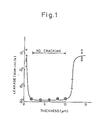
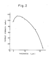
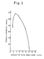
- a process for laser welding a cover and a casing, each made of aluminium or an aluminium based alloy, with a nickel intermediate layer to form a package of electronic devices comprises the steps of: boring holes in sides of the casing, thereby providing holes through which input/output and source terminals can be inserted and be soldered hermetically to the casing; plating a nickel layer on the surface of the casing; mounting electronic devices in the casing and forming connections between the devices and the terminals; and welding the cover and the casing together to seal the cover and the casing hermetically using a pulsed YAG laser beam, thereby forming a weld zone containing 1.5 to 10.0% of nickel by weight.
- the cover and casing may be formed by casting or by cutting of essentially pure aluminium or a cast aluminium based alloy, or a corrosion resistant aluminium based alloy or other aluminium based alloy.
- a pure aluminium may be, e.g. A 1100 as defined in Japanese Industrial Standard (JIS) H 4000.
- a cast aluminium based alloy may be, e.g. AC4A alloy, which contains, in percentage by weight ⁇ 0.2 Cu, 8.0 to 10.0 Si, 0.2 to 0.8 Mg, ⁇ 0.2 Zn, ⁇ 0.7 Fe, 0.3 to 0.8 Mn, ⁇ 0.2 Ti.
- a corrosion resistant aluminium based alloy may be, e.g., A 5052 alloy which contains, in percentage by weight, ⁇ 0.45 (Si + Fe), ⁇ 0.10 Cu, ⁇ 0.10 Mn, 2.2 to 2.8 Mg, 0.15 to 0.35 Cr, ⁇ 0.10 Zn. Both of these alloys are defined also in JIS H 4000.
- a cover 1 and a casing 2 having a side thickness of 2.5 mm were produced of A 1100 pure aluminium.
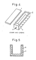
- Two holes for inserting input/output terminals 3 were bored in the end side surfaces of the casing, and twenty four holes for inserting source terminals 4 were bored in the longitudinal side surface of the casing, as shown in Figure 4.
- the casing 2 was chemically plated by means of a plating solution which comprised nickel sulfate 350 g/l, nickel chloride 50 g/l, and boron sulfate 10 g/l, as shown in Figure 5.
- Gallium arsenic FET devices were mounted in the recess of the casing, and the input/output terminals 3 and source terminals 4 were inserted in the side wall of the casing and were soldered to the casing hermetically.
- the nickel layer 5 exhibited a good underplating for soldering. The necessary connections were accomplished between the electronic devices and the terminals.
- the cover 1 and casing 2 were butted together via plated nickel layer 5.
- the laser welding was carried out in nitrogen with a welding speed of 4 mm/s by a 0.3 mm laser beam with an average output of 200 W, a pulse width of 4 ms, and a pulse rate of 15 p/s.
Landscapes
- Physics & Mathematics (AREA)
- Optics & Photonics (AREA)
- Engineering & Computer Science (AREA)
- Mechanical Engineering (AREA)
- Plasma & Fusion (AREA)
- Laser Beam Processing (AREA)
Priority Applications (1)
| Application Number | Priority Date | Filing Date | Title |
|---|---|---|---|
| EP87303537A EP0287722A1 (fr) | 1987-04-22 | 1987-04-22 | Procédé pour le soudage au laser d'éléments à base d'aluminium |
Applications Claiming Priority (1)
| Application Number | Priority Date | Filing Date | Title |
|---|---|---|---|
| EP87303537A EP0287722A1 (fr) | 1987-04-22 | 1987-04-22 | Procédé pour le soudage au laser d'éléments à base d'aluminium |
Publications (1)
| Publication Number | Publication Date |
|---|---|
| EP0287722A1 true EP0287722A1 (fr) | 1988-10-26 |
Family
ID=8197872
Family Applications (1)
| Application Number | Title | Priority Date | Filing Date |
|---|---|---|---|
| EP87303537A Withdrawn EP0287722A1 (fr) | 1987-04-22 | 1987-04-22 | Procédé pour le soudage au laser d'éléments à base d'aluminium |
Country Status (1)
| Country | Link |
|---|---|
| EP (1) | EP0287722A1 (fr) |
Cited By (7)
| Publication number | Priority date | Publication date | Assignee | Title |
|---|---|---|---|---|
| EP0379431A1 (fr) * | 1989-01-20 | 1990-07-25 | Dassault Electronique | Procédé de scellement verre-aluminium, notamment pour traversée électrique de boîtier de circuit hybride, objet composite et composition de verre correspondants |
| WO1995008842A1 (fr) * | 1993-09-22 | 1995-03-30 | Unisys Corporation | Boitier de circuit integre avec un couvercle specialement conçu pour etre assujetti au laser |
| US20140084752A1 (en) * | 2012-09-26 | 2014-03-27 | Seiko Epson Corporation | Method of manufacturing electronic device, electronic apparatus, and mobile apparatus |
| US20140146451A1 (en) * | 2012-11-26 | 2014-05-29 | Seiko Epson Corporation | Method for manufacturing electronic device, cover body, electronic device, electronic apparatus, and moving object |
| CN103846549A (zh) * | 2012-11-29 | 2014-06-11 | 北京航星机器制造公司 | 一种电子成件及电子产品壳的激光焊接封装方法 |
| WO2016005172A1 (fr) * | 2014-07-08 | 2016-01-14 | Continental Automotive Gmbh | Boîtier pour appareil de commande |
| CN116441711A (zh) * | 2023-02-28 | 2023-07-18 | 大族激光科技产业集团股份有限公司 | 7系铝合金的激光焊接方法、激光焊接设备及存储介质 |
Citations (2)
| Publication number | Priority date | Publication date | Assignee | Title |
|---|---|---|---|---|
| US4270986A (en) * | 1979-07-12 | 1981-06-02 | Sifco Industries, Inc. | Method for soldering aluminum |
| US4521668A (en) * | 1983-11-08 | 1985-06-04 | Westinghouse Electric Corp. | Method of hermetically laser sealing electronic packages |
-
1987
- 1987-04-22 EP EP87303537A patent/EP0287722A1/fr not_active Withdrawn
Patent Citations (2)
| Publication number | Priority date | Publication date | Assignee | Title |
|---|---|---|---|---|
| US4270986A (en) * | 1979-07-12 | 1981-06-02 | Sifco Industries, Inc. | Method for soldering aluminum |
| US4521668A (en) * | 1983-11-08 | 1985-06-04 | Westinghouse Electric Corp. | Method of hermetically laser sealing electronic packages |
Non-Patent Citations (1)
| Title |
|---|
| PATENT ABSTRACTS OF JAPAN, vol. 10, no. 151 (M-483)[2208], 31st May 1986; & JP-A-61 003 694 (FUJITSU K.K.) 09-01-1986 * |
Cited By (15)
| Publication number | Priority date | Publication date | Assignee | Title |
|---|---|---|---|---|
| EP0379431A1 (fr) * | 1989-01-20 | 1990-07-25 | Dassault Electronique | Procédé de scellement verre-aluminium, notamment pour traversée électrique de boîtier de circuit hybride, objet composite et composition de verre correspondants |
| FR2642257A1 (fr) * | 1989-01-20 | 1990-07-27 | Dassault Electronique | Procede de scellement verre-aluminium, notamment pour traversee electrique de boitier de circuit hybride, objet composite et composition de verre correspondants |
| US5538527A (en) * | 1989-01-20 | 1996-07-23 | Dassault Electronique | Method of sealing glass to aluminum, particularly for electrical feed-through connectors |
| WO1995008842A1 (fr) * | 1993-09-22 | 1995-03-30 | Unisys Corporation | Boitier de circuit integre avec un couvercle specialement conçu pour etre assujetti au laser |
| US20140084752A1 (en) * | 2012-09-26 | 2014-03-27 | Seiko Epson Corporation | Method of manufacturing electronic device, electronic apparatus, and mobile apparatus |
| US9660176B2 (en) * | 2012-09-26 | 2017-05-23 | Seiko Epson Corporation | Method of manufacturing electronic device, electronic apparatus, and mobile apparatus |
| US9350318B2 (en) * | 2012-11-26 | 2016-05-24 | Seiko Epson Corporation | Method for manufacturing electronic device, cover body, electronic device, electronic apparatus, and moving object |
| US20140146451A1 (en) * | 2012-11-26 | 2014-05-29 | Seiko Epson Corporation | Method for manufacturing electronic device, cover body, electronic device, electronic apparatus, and moving object |
| CN103846549B (zh) * | 2012-11-29 | 2016-02-10 | 北京航星机器制造公司 | 一种电子成件及电子产品壳体的激光焊接封装方法 |
| CN103846549A (zh) * | 2012-11-29 | 2014-06-11 | 北京航星机器制造公司 | 一种电子成件及电子产品壳的激光焊接封装方法 |
| WO2016005172A1 (fr) * | 2014-07-08 | 2016-01-14 | Continental Automotive Gmbh | Boîtier pour appareil de commande |
| CN106470793A (zh) * | 2014-07-08 | 2017-03-01 | 大陆汽车有限公司 | 用于控制单元的壳体 |
| US10421421B2 (en) | 2014-07-08 | 2019-09-24 | Continental Automotive Gmbh | Housing for a control unit |
| DE102014213243B4 (de) | 2014-07-08 | 2024-10-17 | Vitesco Technologies GmbH | Gehäuse für ein Steuergerät |
| CN116441711A (zh) * | 2023-02-28 | 2023-07-18 | 大族激光科技产业集团股份有限公司 | 7系铝合金的激光焊接方法、激光焊接设备及存储介质 |
Similar Documents
| Publication | Publication Date | Title |
|---|---|---|
| US4760240A (en) | Process for laser welding of aluminum based elements | |
| EP0522687B1 (fr) | Connecteur hermétique | |
| US3482305A (en) | Method of bonding aluminum | |
| US4506108A (en) | Copper body power hybrid package and method of manufacture | |
| US6231691B1 (en) | Lead-free solder | |
| EP0568568B1 (fr) | Procede de brasage de surfaces metalliques | |
| KR20060015749A (ko) | 알루미늄재의 납땜방법 | |
| EP0491959B1 (fr) | Procede de soudage de metaux de types differents au moyen d'une energie laser | |
| KR20060123217A (ko) | 브레이징용 알루미늄 합금 스트립 | |
| US20040023487A1 (en) | Electronic component package and method of manufacturing same | |
| Jacobson et al. | Diffusion soldering | |
| JPH02196074A (ja) | セラミックスと金属の接合体の製造法 | |
| JPH08218137A (ja) | レーザー溶接性に優れた銅または銅合金部材 | |
| JPH07223090A (ja) | アルミニウム合金と銅の接合用ろう材およびこのろう材によって接合された複合材 | |
| EP0366082A2 (fr) | Support pour dispositif semi-conducteur | |
| US3553825A (en) | Method of bonding aluminum | |
| JPH0574977A (ja) | アルミナ基体の亀裂を無くす方法 | |
| CN118951479A (zh) | 一种提升铝/铜焊接接头强韧性和耐蚀性的焊料 | |
| Iikawa et al. | Aluminum alloy package for microwave amplifier | |
| Sakai et al. | A new laser hermetic sealing technique for aluminum package | |
| Biro et al. | The effects of Ni and Au/Ni platings on laser welding of thin sheets | |
| JP7586449B2 (ja) | 封止構造体の製造方法 | |
| JPH0947895A (ja) | ろう材 | |
| JPS6325501B2 (fr) | ||
| SU1479246A1 (ru) | Способ диффузионной сварки через промежуточную прокладку |
Legal Events
| Date | Code | Title | Description |
|---|---|---|---|
| PUAI | Public reference made under article 153(3) epc to a published international application that has entered the european phase |
Free format text: ORIGINAL CODE: 0009012 |
|
| AK | Designated contracting states |
Kind code of ref document: A1 Designated state(s): DE FR GB IT NL |
|
| 17P | Request for examination filed |
Effective date: 19881013 |
|
| 17Q | First examination report despatched |
Effective date: 19890323 |
|
| STAA | Information on the status of an ep patent application or granted ep patent |
Free format text: STATUS: THE APPLICATION IS DEEMED TO BE WITHDRAWN |
|
| 18D | Application deemed to be withdrawn |
Effective date: 19890803 |
|
| RIN1 | Information on inventor provided before grant (corrected) |
Inventor name: NAGAI, TAKESHI Inventor name: SAKAI, TAKEAKI Inventor name: NATORI, KATSUHIDE Inventor name: IIKAWA, TSUTOMU Inventor name: KAWAMURA, ISAO Inventor name: OKAMOTO, SHIGEKI |