EP0288007A2 - Appareil générateur de signaux utilisant un circuit à boucle d'asservissement de phase - Google Patents
Appareil générateur de signaux utilisant un circuit à boucle d'asservissement de phase Download PDFInfo
- Publication number
- EP0288007A2 EP0288007A2 EP88106225A EP88106225A EP0288007A2 EP 0288007 A2 EP0288007 A2 EP 0288007A2 EP 88106225 A EP88106225 A EP 88106225A EP 88106225 A EP88106225 A EP 88106225A EP 0288007 A2 EP0288007 A2 EP 0288007A2
- Authority
- EP
- European Patent Office
- Prior art keywords
- signal
- frequency
- mixer
- vco
- switching
- Prior art date
- Legal status (The legal status is an assumption and is not a legal conclusion. Google has not performed a legal analysis and makes no representation as to the accuracy of the status listed.)
- Withdrawn
Links
Images



Classifications
-
- H—ELECTRICITY
- H03—ELECTRONIC CIRCUITRY
- H03L—AUTOMATIC CONTROL, STARTING, SYNCHRONISATION OR STABILISATION OF GENERATORS OF ELECTRONIC OSCILLATIONS OR PULSES
- H03L7/00—Automatic control of frequency or phase; Synchronisation
- H03L7/06—Automatic control of frequency or phase; Synchronisation using a reference signal applied to a frequency- or phase-locked loop
- H03L7/16—Indirect frequency synthesis, i.e. generating a desired one of a number of predetermined frequencies using a frequency- or phase-locked loop
- H03L7/20—Indirect frequency synthesis, i.e. generating a desired one of a number of predetermined frequencies using a frequency- or phase-locked loop using a harmonic phase-locked loop, i.e. a loop which can be locked to one of a number of harmonically related frequencies applied to it
Definitions
- This invention relates to a signal generating apparatus and, more particularly, to a signal generating apparatus using a phase locked loop (PLL) circuit for causing a voltage controlled oscillator (VCO) included in the PLL circuit to generate, in a series of steps, and in a substantially continuous manner, signals having desired frequencies within a predetermined frequency bandwidth.
- PLL phase locked loop
- VCO voltage controlled oscillator
- a signal generating apparatus which uses a PLL circuit is an example of a known conventional signal generating apparatus which can generate signals in the manner described above.
- Fig. 1 shows an example of this type of conventional signal generating apparatus in which an output signal from voltage controlled oscillator 11, contained in the PLL circuit, and a local oscillation signal (frequency fL) from local oscillator 20 are mixed with each other by mixer 12, and the resulting composite signal is fed back to phase detector 14 through low-pass filter 13.
- an output signal from voltage controlled oscillator 11, contained in the PLL circuit, and a local oscillation signal (frequency fL) from local oscillator 20 are mixed with each other by mixer 12, and the resulting composite signal is fed back to phase detector 14 through low-pass filter 13.
- reference signal fr1 is a high-precision signal supplied from reference signal generator 10.
- the PLL circuit functions such that a phase locked relationship is established between reference signal fr1 and composite signal fr2 (or output signal fv and local oscillation signal fL) at a point where composite signal fr2 has always frequency n ⁇ ⁇ f, thereby generating signal having desired frequency fv.
- a signal generating apparatus using a PLL circuit which includes a reference signal generator, a phase detector, a voltage controlled oscillator (VCO), a mixer, and a local oscillator, for generating a signal having a desired frequency within a predetermined frequency bandwidth
- said apparatus further comprises: switching means for performing a switching operation to connect an output terminal of the phase detector to an input terminal of the VCO in a first state, and connect an output terminal of the mixer to an input terminal of the VCO in a second state; and control means, connected to the switching means, for selectively supplying first and second switching signals to the switch means so as to establish connection relationships corresponding to the first and second states, the control means substantially determining a coincidence between a frequency of an output signal from the VCO and a frequency of a local oscillation signal from the local oscillator so as to generate the first switching signal for establishing the connection relationship corresponding to the
- a PLL type signal generating apparatus is realized with a possibly simple arrangement.
- the signal generating apparatus continuously generates a signal having a desired frequency with predetermined steps within a relatively wide frequency bandwidth (e.g., 520 to 1,070 MHz).
- a specific bandwidth becomes as wide as 250 MHz.
- local oscillation signal fL is preferably set in a narrowest bandwidth in substantially a central range of the entire frequency range, it is set at 770 to 820 MHz (a specific bandwidth of 50 MHz) in the above case.
- phase detector in the PLL circuit is inevitably set in the inoperative state due to the dead band.
- n 0 and a signal obtained by mixing an output signal from the voltage controlled oscillator with a local oscillation signal from the local oscillator, i.e., a DC signal, is output from the mixer to be supplied to the phase detector as a feedback signal, the following problems are posed. Since the phase detector is not operated by a DC signal, a separate circuit capable of performing comparison must be added to the PLL circuit. In addition, a DC reference signal must be output. Moreover, signals including high-frequency to DC signals must be stably transmitted between the mixer and the phase detector. That is, in order to solve these problems, a phase detector, a DC comparator, a reference signal amplifier, and the like must be additionally arranged in the PLL circuit and each constituent circuit must be switched. However, such a solution is not preferable because it makes the circuit arrangement complex.
- the present invention has been made in consideration of the various problems described above.
- the arrangement of the present invention is characterized in that stable signals having desired frequencies with predetermined steps can be substantially continuously generated within a predetermined bandwidth by selectively switching and supplying output signals from the mixer to first and second feedback paths in accordance with switching signals corresponding to set frequencies.
- the switching unit switches the output from the mixer to the phase detector side in accordance with the switching signal from the controller. Then, the phase detector compares the phase of the output from the mixer with that of a reference signal and supplies a signal based on this comparison result to the voltage controlled oscillator so as to control its oscillation frequency. As a result, the voltage controlled oscillator outputs a signal having a desired frequency in the range for n ⁇ 0.
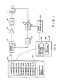
- Fig. 3 is a block diagram of a signal generating apparatus according a first embodiment of the present invention.
- a PLL type signal generating apparatus comprises reference signal generator 10A, phase detector 14, DC amplifier 15, loop (low-pass) filter 16, voltage controlled oscillator 11, mixer 12, low-pass filter 13, switching unit 17, low-pass filter 18, controller 19, and local oscillator 20.
- An output signal from mixer 12 is selectively switched and supplied to phase detector 14 side or directly to voltage controlled oscillator 11 side by switching unit 17 operated by a switching signal output from controller 19. With this operation, feedback path I or is determined, and voltage controlled oscillator 11 substantially continuously generates signals having desired frequencies with predetermined steps within a predetermined frequency bandwidth, e.g., 570 to 1,070 MHz.
- the predetermined steps mean a frequency resolution which can be set and is determined in such a manner that setting section 19a in controller 19, which will be described in detail later, sets a value of 1 Hz or 10 Hz as a minimum unit of frequency in local oscillator 20 in accordance with, e.g., a key operation.
- DC amplifier 15 and loop filter 16 process the low-frequency error signal supplied from phase detector 14 and supply the resultant signal to voltage controlled oscillator 11.
- a loop-response damping factor is determined by variable gain control and the filter effect. For example, when the apparatus outputs a signal other than a signal having a desired frequency determined by setting section 19a because of noise generated when a switching operation is performed by switching unit 17, DC amplifier 15 and loop filter 16 variably control a loop response speed, a lock range, and the like so as to cause the apparatus to restore the normal operation and output a signal having a desired frequency.
- Mixer 12 mixes the feedback signal from voltage controlled oscillator 11 with local oscillation signal fL, which is supplied from local oscillator 20 and corresponds to a desired frequency variably set by setting section 19a in controller 19 to be described later.
- the functions of mixer 12 are selectively switched in accordance with the value of local oscillation signal fL, i.e., substantially the value of frequency index n . More specifically, when n ⁇ 0, mixer 12 functions as a normal mixer for mixing feedback signal fv with local oscillation signal fL, and supplying composite signal fr2 to phase detector 14 through low-pass filter 13.
- mixer 12 when mixer 12 causes voltage controlled oscillator 11 to output a signal having a desired frequency within a bandwidth of 520 to 770 MHz while inequality fL ⁇ fv is satisfied, mixer 12 adds feedback signal fv to local oscillation signal fL.
- mixer 12 subtracts feedback signal fv from local oscillation signal fL.
- mixer 12 compares the phases of feedback signal fv and local oscillation signal fL with each other in the same manner as in phase detector 14, and supplies a signal based on this comparison result to voltage controlled oscillator 11 through low-pass filter 18, switching unit 17, DC amplifier 15, and loop filter 16, thereby controlling the oscillation frequency of voltage controlled oscillator 11.
- voltage controlled oscillator 11 outputs a signal having a desired frequency within a bandwidth of 770 to 820 MHz.
- Low-pass filter 13 eliminates a high-frequency component of the composite signal supplied from mixer 12 when n ⁇ 0.
- the composite signal free from high-frequency component is supplied to phase detector 14.
- switching unit 17 switches the feedback paths in accordance with the value of n .
- switching unit 17 is normally switched so as to select feedback path I .
- switching unit 17 is switched so as to select feedback path .
- Controller 19 comprises setting section 19 and ALU section 19b.
- These input setting operations are performed by a ten-key pad or the like (not shown) arranged on a panel of the apparatus.
- ALU section 19b controls a drive operation of each circuit within the loop. Note that reference symbols A1 and A2 in Fig. 3 respectively denote compensating amplifiers.
- feedback path I is set by ALU section 19b in accordance with a frequency setting operation, and local oscillation signal fL supplied to mixer 12 and position n (n > 1 to 5: inteS ger) of switch SWa in reference signal generator 10 are variably set by setting section 19a. Then, feedback signal fv from voltage controlled oscillator 11 and local oscillation signal fL are added/mixed by mixer 12. The resultant composite signal is supplied to phase detector 14 through low-pass filter 13.
- Phase detector 14 receives composite signal fr2 and supplies to voltage controlled oscillator 11 an error signal proportional to the phase difference between composite signal fr2 and a reference signal through switching unit 17, DC amplifier 15, and loop filter 16.
- the oscillation frequency of voltage controlled oscillator 11 is controlled by the error signal, and a signal having a desired frequency is output within a bandwidth of 520 to 770 MHz.
- a desired signal can be obtained in the same manner as described above except that a difference between feedback signal fv from voltage controlled oscillator 11 and local oscillation signal fL from local oscillator 20 is calculated by mixer 12.
- n 0 wherein a signal having a desired frequency is to be generated by voltage controlled oscillator 11 within a bandwidth of 770 to 820 MHz
- feedback path I is switched to feedback path .
- local oscillation signal fL to be supplied to mixer 12 is variably set, the phases of feedback signal fv from voltage controlled oscillator 11 and local oscillation signal fL are compared with each other in mixer 12.
- a signal (a DC voltage signal) based on this comparison result is supplied to voltage controlled oscillator 11 through low-pass filter 18, switching unit 17, DC amplifier 15, and loop filter 16.
- the oscillation frequency of voltage controlled oscillator 11 is controlled by the above-described DC voltage signal and a signal having a desired frequency in a bandwidth of 770 to 820 MHz is output.
- Fig. 5 shows a second embodiment, in which the same reference numerals denote the same constituent elements as in Fig. 3.
- low-pass filters 13 and 18, and compensating amplifiers A1 and A2 in Fig. 3, which are not essential elements, are omitted.
- Local oscillator 20A constitutes a continuous oscillator having ⁇ f width of, e.g., 770 to 820 MHz and includes lower-digit variable synthesizer 201 for outputting a local oscillation signal obtained by interpolating 88 to 138 MHz in 10-Hz steps, and mixer 202.
- An FM signal from FM source 20B constituted by 600-MHz fixed oscillator 203, 82-MHz FM modulation signal source 204, and mixer 205 is supplied to mixer 202, as needed.
- An local oscillation signal from local oscillator 20B with such an arrangement is supplied to mixer 12 through 770- to 820-MHz bandpass filter 21.
- Fig. 6 is a flow chart for explaining an operation in Fig. 5.
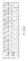
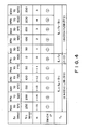
- the contents in Fig. 4 are stored in a memory section in the form of a table in controller 19 constituted by a CPU.
- reference signal fr1 is set at 150 MHz, and then switching unit 17 is set to the feedback path I side.
- controller 19 may performs a predetermined operation using ALU section 19b.
- the output from lower-digit variable synthesizer 201 and the high-frequency output obtained by mixer 205 are added to each other by mixer 202, thereby obtaining local oscillation signal fL. Therefore, the upper limit oscillation frequency of lower-digit variable synthesizer 201 can be minimized to a low frequency. Consequently, the size of a PLL circuit using the lower-digit synthesizer can be reduced while a lower-digit synthesizer capable of relatively easily increasing the number of set digits can be realized.
- this lower-digit synthesizer is required to perform only interpolation between ⁇ f, the specific bandwidth of the oscillation frequency of the VCO in the PLL circuit used therein can be restricted to two times (actually 1.5 times). As a result, even if variations in constants of parts to be used are considered, a sufficiently stable variable range (specific bandwidth) of the oscillation frequency can be assured.
- a high-frequency filter specifically, bandpass filter 21
- the signal generating apparatus can achieve excellent signal purity and frequency stability in state of non-PLL (free-running state).
- the switching unit selectively switches an output from the mixer to the phase detector side in the first state, and to the voltage controlled oscillator side in the second state in response to a switching signal from the controller in accordance with a frequency setting operation, and hence the output from the mixer can be switched to the first or second feedback path.
- the signal generating apparatus utilizes the fact that the mixer can be operated as a phase detector, the apparatus can be maximally simplified and realized at low cost without complicating the circuit arrangement.
Landscapes
- Stabilization Of Oscillater, Synchronisation, Frequency Synthesizers (AREA)
Applications Claiming Priority (2)
| Application Number | Priority Date | Filing Date | Title |
|---|---|---|---|
| JP9507987 | 1987-04-20 | ||
| JP95079/87 | 1987-04-20 |
Publications (2)
| Publication Number | Publication Date |
|---|---|
| EP0288007A2 true EP0288007A2 (fr) | 1988-10-26 |
| EP0288007A3 EP0288007A3 (fr) | 1990-03-28 |
Family
ID=14127951
Family Applications (1)
| Application Number | Title | Priority Date | Filing Date |
|---|---|---|---|
| EP88106225A Withdrawn EP0288007A3 (fr) | 1987-04-20 | 1988-04-19 | Appareil générateur de signaux utilisant un circuit à boucle d'asservissement de phase |
Country Status (2)
| Country | Link |
|---|---|
| US (1) | US4862106A (fr) |
| EP (1) | EP0288007A3 (fr) |
Families Citing this family (8)
| Publication number | Priority date | Publication date | Assignee | Title |
|---|---|---|---|---|
| EP0364679B1 (fr) * | 1988-10-18 | 1994-11-02 | Siemens-Albis Aktiengesellschaft | Appareil synthétiseur de fréquence |
| US5349613A (en) * | 1991-05-08 | 1994-09-20 | U.S. Philips Corporation | Digital phase locked loop, and digital oscillator arranged to be used in the digital phase locked loop |
| US5239271A (en) * | 1991-11-01 | 1993-08-24 | Ben Efraim Gideon | Microwave synthesizer |
| KR100193862B1 (ko) * | 1996-03-19 | 1999-06-15 | 윤종용 | 안정된 주파수를 얻기 위한 주파수변환기 |
| JP4401011B2 (ja) * | 2000-08-04 | 2010-01-20 | Necエレクトロニクス株式会社 | Pll回路 |
| ATE422729T1 (de) * | 2000-12-28 | 2009-02-15 | Renesas Tech Corp | Pll-schaltung mit reduzierter einschwingzeit |
| US7119583B2 (en) * | 2004-03-31 | 2006-10-10 | Micron Technology, Inc. | Phase detector and method having hysteresis characteristics |
| US7423456B2 (en) * | 2006-12-01 | 2008-09-09 | Micron Technology, Inc. | Fast response time, low power phase detector circuits, devices and systems incorporating the same, and associated methods |
Family Cites Families (4)
| Publication number | Priority date | Publication date | Assignee | Title |
|---|---|---|---|---|
| JPS5854683B2 (ja) * | 1978-11-28 | 1983-12-06 | 安立電気株式会社 | Pll周波数シンセサイザ |
| FR2497425B1 (fr) * | 1980-12-31 | 1985-10-31 | Adret Electronique | Synthetiseur de frequence a multiplicateur fractionnaire |
| DE3122274A1 (de) * | 1981-06-04 | 1982-12-23 | Siemens AG, 1000 Berlin und 8000 München | Oszillatorschaltung mit einem ersten frei durchstimmbaren oszillator und mindestens einem zweiten quarzstabilisierten oszillator |
| GB2209442A (en) * | 1987-09-04 | 1989-05-10 | Marconi Instruments Ltd | Frequency synthesizer |
-
1988
- 1988-04-19 EP EP88106225A patent/EP0288007A3/fr not_active Withdrawn
- 1988-04-20 US US07/183,827 patent/US4862106A/en not_active Expired - Fee Related
Also Published As
| Publication number | Publication date |
|---|---|
| US4862106A (en) | 1989-08-29 |
| EP0288007A3 (fr) | 1990-03-28 |
Similar Documents
| Publication | Publication Date | Title |
|---|---|---|
| US5825252A (en) | Synthesized oscillation circuit | |
| US5140284A (en) | Broad band frequency synthesizer for quick frequency retuning | |
| US5152005A (en) | High resolution frequency synthesis | |
| US4211975A (en) | Local signal generation arrangement | |
| CA2125443C (fr) | Circuit pour oscillateur controlable | |
| US5831481A (en) | Phase lock loop circuit having a broad loop band and small step frequency | |
| CA2010176A1 (fr) | Dispositif de syntonisation | |
| US4603304A (en) | Reference frequency generation for split-comb frequency synthesizer | |
| EP0622904B1 (fr) | Circuit PLL comportant plusieurs boucles, méthode de réception de signaux FM et dispositif les mettant en oeuvre | |
| EP0288007A2 (fr) | Appareil générateur de signaux utilisant un circuit à boucle d'asservissement de phase | |
| US6239660B1 (en) | Step-controlled frequency synthesizer | |
| US4459560A (en) | Plural phase locked loop frequency synthesizer | |
| US4963838A (en) | Frequency synthesizer | |
| JPH0946225A (ja) | マイクロ波・ミリ波帯位相同期発振回路 | |
| US4797637A (en) | PLL frequency synthesizer | |
| US4186356A (en) | Phase locked loop frequency synthesizer and frequency modulator | |
| JP2830815B2 (ja) | Pll周波数シンセサイザ | |
| JPH1079666A (ja) | 位相同期発振回路 | |
| JP2853817B2 (ja) | フェイズロックループ | |
| JP3260567B2 (ja) | クロック生成回路 | |
| JP2631009B2 (ja) | Pll回路 | |
| JP3248453B2 (ja) | 発振装置 | |
| JPH06291645A (ja) | 周波数シンセサイザ | |
| JPS6359008A (ja) | Fm変調回路 | |
| KR960011423B1 (ko) | 주파수 합성시 잡음억제 방법 |
Legal Events
| Date | Code | Title | Description |
|---|---|---|---|
| PUAI | Public reference made under article 153(3) epc to a published international application that has entered the european phase |
Free format text: ORIGINAL CODE: 0009012 |
|
| AK | Designated contracting states |
Kind code of ref document: A2 Designated state(s): DE GB |
|
| PUAL | Search report despatched |
Free format text: ORIGINAL CODE: 0009013 |
|
| AK | Designated contracting states |
Kind code of ref document: A3 Designated state(s): DE GB |
|
| 17P | Request for examination filed |
Effective date: 19900607 |
|
| 17Q | First examination report despatched |
Effective date: 19920903 |
|
| STAA | Information on the status of an ep patent application or granted ep patent |
Free format text: STATUS: THE APPLICATION IS DEEMED TO BE WITHDRAWN |
|
| 18D | Application deemed to be withdrawn |
Effective date: 19930216 |