EP0288052A2 - Semiconductor device comprising a substrate, and production method thereof - Google Patents
Semiconductor device comprising a substrate, and production method thereof Download PDFInfo
- Publication number
- EP0288052A2 EP0288052A2 EP88106396A EP88106396A EP0288052A2 EP 0288052 A2 EP0288052 A2 EP 0288052A2 EP 88106396 A EP88106396 A EP 88106396A EP 88106396 A EP88106396 A EP 88106396A EP 0288052 A2 EP0288052 A2 EP 0288052A2
- Authority
- EP
- European Patent Office
- Prior art keywords
- semiconductor device
- semiconductor chip
- compound semiconductor
- concave portion
- silicon substrate
- Prior art date
- Legal status (The legal status is an assumption and is not a legal conclusion. Google has not performed a legal analysis and makes no representation as to the accuracy of the status listed.)
- Ceased
Links
Images
Classifications
-
- H—ELECTRICITY
- H10—SEMICONDUCTOR DEVICES; ELECTRIC SOLID-STATE DEVICES NOT OTHERWISE PROVIDED FOR
- H10P—GENERIC PROCESSES OR APPARATUS FOR THE MANUFACTURE OR TREATMENT OF DEVICES COVERED BY CLASS H10
- H10P50/00—Etching of wafers, substrates or parts of devices
- H10P50/60—Wet etching
- H10P50/64—Wet etching of semiconductor materials
- H10P50/642—Chemical etching
- H10P50/644—Anisotropic liquid etching
-
- H—ELECTRICITY
- H10—SEMICONDUCTOR DEVICES; ELECTRIC SOLID-STATE DEVICES NOT OTHERWISE PROVIDED FOR
- H10W—GENERIC PACKAGES, INTERCONNECTIONS, CONNECTORS OR OTHER CONSTRUCTIONAL DETAILS OF DEVICES COVERED BY CLASS H10
- H10W20/00—Interconnections in chips, wafers or substrates
- H10W20/40—Interconnections external to wafers or substrates, e.g. back-end-of-line [BEOL] metallisations or vias connecting to gate electrodes
-
- H—ELECTRICITY
- H10—SEMICONDUCTOR DEVICES; ELECTRIC SOLID-STATE DEVICES NOT OTHERWISE PROVIDED FOR
- H10W—GENERIC PACKAGES, INTERCONNECTIONS, CONNECTORS OR OTHER CONSTRUCTIONAL DETAILS OF DEVICES COVERED BY CLASS H10
- H10W70/00—Package substrates; Interposers; Redistribution layers [RDL]
- H10W70/01—Manufacture or treatment
- H10W70/05—Manufacture or treatment of insulating or insulated package substrates, or of interposers, or of redistribution layers
- H10W70/093—Connecting or disconnecting other interconnections thereto or therefrom, e.g. connecting bond wires or bumps
-
- H—ELECTRICITY
- H10—SEMICONDUCTOR DEVICES; ELECTRIC SOLID-STATE DEVICES NOT OTHERWISE PROVIDED FOR
- H10W—GENERIC PACKAGES, INTERCONNECTIONS, CONNECTORS OR OTHER CONSTRUCTIONAL DETAILS OF DEVICES COVERED BY CLASS H10
- H10W70/00—Package substrates; Interposers; Redistribution layers [RDL]
- H10W70/60—Insulating or insulated package substrates; Interposers; Redistribution layers
-
- H—ELECTRICITY
- H10—SEMICONDUCTOR DEVICES; ELECTRIC SOLID-STATE DEVICES NOT OTHERWISE PROVIDED FOR
- H10W—GENERIC PACKAGES, INTERCONNECTIONS, CONNECTORS OR OTHER CONSTRUCTIONAL DETAILS OF DEVICES COVERED BY CLASS H10
- H10W70/00—Package substrates; Interposers; Redistribution layers [RDL]
- H10W70/60—Insulating or insulated package substrates; Interposers; Redistribution layers
- H10W70/67—Insulating or insulated package substrates; Interposers; Redistribution layers characterised by their insulating layers or insulating parts
- H10W70/68—Shapes or dispositions thereof
-
- H—ELECTRICITY
- H10—SEMICONDUCTOR DEVICES; ELECTRIC SOLID-STATE DEVICES NOT OTHERWISE PROVIDED FOR
- H10W—GENERIC PACKAGES, INTERCONNECTIONS, CONNECTORS OR OTHER CONSTRUCTIONAL DETAILS OF DEVICES COVERED BY CLASS H10
- H10W70/00—Package substrates; Interposers; Redistribution layers [RDL]
- H10W70/60—Insulating or insulated package substrates; Interposers; Redistribution layers
- H10W70/67—Insulating or insulated package substrates; Interposers; Redistribution layers characterised by their insulating layers or insulating parts
- H10W70/69—Insulating materials thereof
- H10W70/698—Semiconductor materials that are electrically insulating, e.g. undoped silicon
-
- H—ELECTRICITY
- H10—SEMICONDUCTOR DEVICES; ELECTRIC SOLID-STATE DEVICES NOT OTHERWISE PROVIDED FOR
- H10W—GENERIC PACKAGES, INTERCONNECTIONS, CONNECTORS OR OTHER CONSTRUCTIONAL DETAILS OF DEVICES COVERED BY CLASS H10
- H10W70/00—Package substrates; Interposers; Redistribution layers [RDL]
- H10W70/60—Insulating or insulated package substrates; Interposers; Redistribution layers
- H10W70/67—Insulating or insulated package substrates; Interposers; Redistribution layers characterised by their insulating layers or insulating parts
- H10W70/68—Shapes or dispositions thereof
- H10W70/682—Shapes or dispositions thereof comprising holes having chips therein
-
- H—ELECTRICITY
- H10—SEMICONDUCTOR DEVICES; ELECTRIC SOLID-STATE DEVICES NOT OTHERWISE PROVIDED FOR
- H10W—GENERIC PACKAGES, INTERCONNECTIONS, CONNECTORS OR OTHER CONSTRUCTIONAL DETAILS OF DEVICES COVERED BY CLASS H10
- H10W72/00—Interconnections or connectors in packages
- H10W72/01—Manufacture or treatment
- H10W72/0198—Manufacture or treatment batch processes
-
- H—ELECTRICITY
- H10—SEMICONDUCTOR DEVICES; ELECTRIC SOLID-STATE DEVICES NOT OTHERWISE PROVIDED FOR
- H10W—GENERIC PACKAGES, INTERCONNECTIONS, CONNECTORS OR OTHER CONSTRUCTIONAL DETAILS OF DEVICES COVERED BY CLASS H10
- H10W72/00—Interconnections or connectors in packages
- H10W72/071—Connecting or disconnecting
- H10W72/075—Connecting or disconnecting of bond wires
-
- H—ELECTRICITY
- H10—SEMICONDUCTOR DEVICES; ELECTRIC SOLID-STATE DEVICES NOT OTHERWISE PROVIDED FOR
- H10W—GENERIC PACKAGES, INTERCONNECTIONS, CONNECTORS OR OTHER CONSTRUCTIONAL DETAILS OF DEVICES COVERED BY CLASS H10
- H10W90/00—Package configurations
-
- H—ELECTRICITY
- H10—SEMICONDUCTOR DEVICES; ELECTRIC SOLID-STATE DEVICES NOT OTHERWISE PROVIDED FOR
- H10W—GENERIC PACKAGES, INTERCONNECTIONS, CONNECTORS OR OTHER CONSTRUCTIONAL DETAILS OF DEVICES COVERED BY CLASS H10
- H10W90/00—Package configurations
- H10W90/701—Package configurations characterised by the relative positions of pads or connectors relative to package parts
- H10W90/751—Package configurations characterised by the relative positions of pads or connectors relative to package parts of bond wires
- H10W90/754—Package configurations characterised by the relative positions of pads or connectors relative to package parts of bond wires between a chip and a stacked insulating package substrate, interposer or RDL
Definitions
- the present invention relates to a semiconductor device in which a high speed and high integrated compound semiconductor element such as gallium arsenide is used, particularly relates to a semiconductor device which is used in a high speed signal processing, and also relates to a method for producing such a semiconductor device.
- gallium arsenide semiconductor device for performing a high speed signal processing in a high frequency band, particularly in a GHz band and higher frequency band.
- An object of the present invention is to provide a semiconductor device and the production method thereof, wherein the semiconductor device has a sufficiently high density of thin film circuit and has good characteristics of high speed operation.
- the semiconductor device comprises; a compound semiconductor chip which is disposed in a concave portion, a silicon substrate having a first connecting circuit pattern formed on the surface of the silicon substrate and the concave defined on the substrate, said concave being surrounded by surrounding walls, flattening means for covering over a space between the compound semiconductor chip and the surrounding walls to provide a flat surface, and a second connecting circuit pattern formed on the flat surface for connecting between electrodes on the compound semiconductor chip and the first connecting circuit pattern on the silicon substrate.
- the method for producing a semiconductor device comprises; a process of forming a first connecting circuit pattern on a substrate, a process of implanting ion in said substrate in order to form an etching stopper layer in a predetermined depth of said substrate, a process of etching a predetermined area of a silicon substrate up to the etching stopper layer to form a concave portion, a process of accommodating a compound semiconductor chip in the concave portion, a process of forming an insulating film layer for covering the space between the peripheral wall of the concave portion and the side wall of the compound semiconductor chip, and a process of forming a second connecting circuit pattern on the insulating film for connecting between the electrodes on the compound semiconductor chip and said first connecting circuit pattern.
- the etching process for forming the concave portion is performed after the etching stopper is formed in addition, the insulating resin film is formed covering over the space between the surrounding wall of the concave portion of the substrate and the side wall of the compound semiconductor chip, and the thin film connecting circuit pattern is formed on the insulating resin film, therefore, the semiconductor device mentioned above can be surely manufactured without bonding wires.
- Fig. 2(e) shows a plurality of semiconductor chips 50 after separation process by dicing, wherein a concave portion 54 is formed below the upper surface of a silicon substrate 51 on which a first connecting circuit pattern 60 is already formed and a gallium arsenide chip 55 is buried in the concave portion 54 so that the level of the upper surface of the gallium arsenide chip 55 coincides with the level of the upper surface of the silicon substrate 51.
- an insulating resin film 56 on the surface of the gallium arsenide chip 55 and on the surface of the substrate 51, covering over the concave portion 54.
- a thin film circuit layer 57 i.e., a second connecting circuit pattern made of aluminum for example on the insulating film 56.
- bonding pads for wire bonding are unnecessary so that the space for the pads can be omitted, whereby more thin film circuits can be formed in the space corresponding to the space of the pads so that a high density circuit can be provided. Moreover, the lowering of the high frequency characteristic due to the capacity of the wire and the inductance can be prevented.
- a silicon substrate 51 on the crystal orientation (100) surface on which a first connecting circuit pattern 60 is already formed in a predetermined pattern.
- an etching stopper layer 52 by previously implanting ionized boron material in the substrate 51 so as to provide a high dosing density of 7 ⁇ 1019/cm3 as shown in Fig. 2(a).
- a layer 51a above the etching stopper layer 52 may be formed by an epitaxial growth of silicon single crystal after the ionized boron is implanted in the substrate 51.
- the etching stopper layer 52 may be formed by way of deposit and diffusion method.
- a mask 53 made of such as silicon dioxide (SiO2) or silicon nitride (SiN) is formed on the surface of the silicon substrate 51 by patterning and the mask 53 is processed by anisotropic etching with etchant of mixed liquid of ethylenediamine, pyrocatechol and water.
- concave portions 54 each having a side wall 54a of the crystal orientation (111) inclined at an angle of 54.7° to the horizontal surface as shown in Fig. 2(b).
- the depth of the concave portion 54 is approximately 200 ⁇ m.
- the depth of the concave may be controlled by controlling the etching time.
- the mask 53 is removed and a gallium arsenide chip 55 of approximately 180 ⁇ m thick having an integrated circuit pattern (not shown) is disposed in the concave portion 54 so as to provide a diebonding of approximately 20 ⁇ m thick with eutectic crystal alloy of aurum and tin for example.
- the thickness of the gallium arsenide chip 55 and the die-bonding is equal to the depth of the concave portion 54, therefore, the level of the surface of the gallium arsenide chip 55 coincides with the level of the surface of the silicon substrate 51.
- an insulating film 56 made of such as polyimide is coated on the whole surface of the substrate 51 and the surface of the electrodes of the chips 55, then the coated insulating film 56 is patterned so that the electrodes on the gallium arsenide chips 55 and the circuit on the surface of the substrate 51 are exposed.
- the spaces between the surrounding wall 54a of the concave portion 54 and the side wall of the gallium arsenide chip 55 are not usually filled with filler perfectly, since the space are so minute that it is not necessary to fill the spaces perfectly, but the spaces may be also filled perfectly.
- the conducting layer is patterned for forming an upper thin film connecting circuit layer 57 for connecting the electrodes on the gallium arsenide chip 55 and the first connecting circuit pattern 60 previously formed on the surface of the substrate 51.
- the width of the upper thin film connecting circuit pattern 57 is approximately 10 ⁇ m, which is wider than that of a usual thin film circuit, and since there does not occur such a deformation such as occurs in a wire arrangement in the conventional semiconductor device, it is possible to make a thin film circuit having a higher circuit pattern density than that of the conventional device.
- an insulating film such as a silicon nitride film or a silicon dioxide film is coated on the whole part of the surface by plasma CVD method or by ECR sputtering method so as to make a protecting film, and the substrate 51 is fixed onto the base (not shown) of the dicing device with adhesive tape 58. Then, the fixed substrate 51 is cut by means of a dicing bleed so that the substrate 51 is divided into a plurality of separated individual chips 50 as shown in Fig. 2(e).
- the semiconductor chips obtained in this way are die-bonded to the base of a package with eutectic crystal alloy of tin and silver, for example, so as to make a semiconductor package.
- etchant of ethylenediamine group is used for forming the concave portion
- etchant of hydrazine group can be also used, and the material of the mask may be changed in accordance with the kind of the etchant.
- the flattening thin film layer is not limited to polyimide layer and any material having good heat resistance and insulating ability can be used.
- the material of the circuit layer is not limited to aluminum, and various kinds of conductive material can be used.
- the surface of the silicon substrate is not limited to a crystal orientation (100) and when the surface of the silicon substrate is made to be a crystal orientation (110), a hole portion having a side wall vertical to the horizontal surface may be formed by etching process.
- the compound semiconductor chip is disposed in the concave portion formed on the surface of the silicon substrate, and since the compound semiconductor chip is connected to the circuit on the surface of the silicon substrate through the thin film circuit, the time lag of transferring signals due to the circuit capacity which can not be avoided in wire-bonding may be prevented and there is an effect of expanding an area for forming a circuit.
Landscapes
- Internal Circuitry In Semiconductor Integrated Circuit Devices (AREA)
- Wire Bonding (AREA)
- Pressure Sensors (AREA)
- Weting (AREA)
Abstract
Description
- The present invention relates to a semiconductor device in which a high speed and high integrated compound semiconductor element such as gallium arsenide is used, particularly relates to a semiconductor device which is used in a high speed signal processing, and also relates to a method for producing such a semiconductor device.
- In many cases, there has been used a gallium arsenide semiconductor device for performing a high speed signal processing in a high frequency band, particularly in a GHz band and higher frequency band.
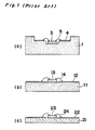
- Fig. 1 shows an example of a conventional packaging type of a semiconductor device in which gallium arsenide is used as a semiconductor element.
- Fig. 1(a) is a sectional view showing an example of a constitution of a conventional gallium arsenide semiconductor device. As shown in Fig. 1(a), there is disposed a
semiconductor chip 3 made of gallium arsenide in a concave portion 2 provided in the central portion of a base 1 made of ceramics such as alumina, and electrodes (not shown) of thegallium arsenide chip 3 are connected to terminals of a thick film printedcircuit 4 formed on the peripheral portion of the concave portion 2 on the base 1 throughbonding wires 5 made of such as aurum material.
However, the surface of the ceramic base 1 is so uneven that it is difficult to form a circuit with high precision thereon. Therefore, the minimum width of a thick film printedcircuit 4 is approximately 100 µ m, resulting in that it is impossible to package a circuit with high density. Particularly, since it is difficult to form a ground circuit for isolation, impedance conformity can not be performed so that the degree of freedom of the connecting circuit pattern is little. - Fig. 1(b) is a sectional view showing another example of packaging type of a conventional semiconductor device. As shown in Fig. 1(b), there is formed a
thin film circuit 12 on the flat upper surface of aceramic base 11, and thethin film circuit 12 is connected throughwires 14 to a galliumarsenide semiconductor chip 13 which is disposed to be die-bonded in the central portion of thebase 11. Even in this case, however, since thebase 11 is made of ceramics, the minimum width of thethin film circuit 12 may be made only approximately 10 µ m so that an integral multi-pack film circuit can not be formed, resulting in that the conventional semiconductor device is not suitable to a package with high density. - Fig. 1(c) is a sectional view showing still more another example of a packaging type of a conventional semiconductor device. As shown in Fig. 1(c), in this case, there is disposed and die-bonded a
gallium arsenide chip 23 in the central portion of the upper surface of asilicon substrate 21 having a thinfilm circuit layer 22 formed on the surface of thesilicon substrate 21. The thinfilm circuit layer 22 is connected to thegallium arsenide chip 23 throughwires 24. In this case, since the flatness of the surface of thesilicon substrate 21 is remarkably improved because of adopting a silicon substrate, the minimum width of the thin film circuit layer may be made approximately 3 µ m. - However, in any case mentioned above, since wires are used for connecting between the gallium arsenide chip and the thin film circuit, there is a limitation thereby so that the sufficient high density of the thin film circuit has not yet accomplished. Moreover, since the wiring device has a circuit capacity, there often occurs a time lag, so that the conventional semiconductor devices as mentioned above are not suitable to high speed operation.
- An object of the present invention is to provide a semiconductor device and the production method thereof, wherein the semiconductor device has a sufficiently high density of thin film circuit and has good characteristics of high speed operation.
- The semiconductor device according to the present invention comprises; a compound semiconductor chip which is disposed in a concave portion, a silicon substrate having a first connecting circuit pattern formed on the surface of the silicon substrate and the concave defined on the substrate, said concave being surrounded by surrounding walls, flattening means for covering over a space between the compound semiconductor chip and the surrounding walls to provide a flat surface, and a second connecting circuit pattern formed on the flat surface for connecting between electrodes on the compound semiconductor chip and the first connecting circuit pattern on the silicon substrate.
- Moreover, the method for producing a semiconductor device comprises; a process of forming a first connecting circuit pattern on a substrate, a process of implanting ion in said substrate in order to form an etching stopper layer in a predetermined depth of said substrate, a process of etching a predetermined area of a silicon substrate up to the etching stopper layer to form a concave portion, a process of accommodating a compound semiconductor chip in the concave portion, a process of forming an insulating film layer for covering the space between the peripheral wall of the concave portion and the side wall of the compound semiconductor chip, and a process of forming a second connecting circuit pattern on the insulating film for connecting between the electrodes on the compound semiconductor chip and said first connecting circuit pattern.
- In the semiconductor device according to the present invention as described above, since a precise thin film circuit is formed without using a wire, a circuit with higher density can be formed, and it is possible to decrease a capacitance of the connecting circuit pattern, thereby assuring a high speed operation of the semiconductor device.
- Moreover, in the method for producing a semiconductor device according to the present invention, the etching process for forming the concave portion is performed after the etching stopper is formed in addition, the insulating resin film is formed covering over the space between the surrounding wall of the concave portion of the substrate and the side wall of the compound semiconductor chip, and the thin film connecting circuit pattern is formed on the insulating resin film, therefore, the semiconductor device mentioned above can be surely manufactured without bonding wires.
-
- Figs. 1(a) to 1(c) are sectional views showing components of conventional gallium arsenide semiconductor devices,
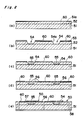
- Figs. 2(a) to 2(e) are sectional views showing each process of manufacturing a semiconductor device according to the present invention.
- One example of a semiconductor device according to the present invention and the production method thereof will be explained with reference to the attached drawings as follows. In the explanation of the drawings, similar numerals are used for the similar parts and the redundant explanations are omitted.
- Fig. 2(e) shows a plurality of
semiconductor chips 50 after separation process by dicing, wherein aconcave portion 54 is formed below the upper surface of asilicon substrate 51 on which a firstconnecting circuit pattern 60 is already formed and agallium arsenide chip 55 is buried in theconcave portion 54 so that the level of the upper surface of thegallium arsenide chip 55 coincides with the level of the upper surface of thesilicon substrate 51. There is formed aninsulating resin film 56 on the surface of thegallium arsenide chip 55 and on the surface of thesubstrate 51, covering over theconcave portion 54. Moreover, there is formed a thinfilm circuit layer 57, i.e., a second connecting circuit pattern made of aluminum for example on theinsulating film 56. Thus, the circuit arrangement formed by wires and wire bonding as in the conventional semiconductor device can be eliminated. - Accordingly, bonding pads for wire bonding are unnecessary so that the space for the pads can be omitted, whereby more thin film circuits can be formed in the space corresponding to the space of the pads so that a high density circuit can be provided. Moreover, the lowering of the high frequency characteristic due to the capacity of the wire and the inductance can be prevented.
- Next, the process of producing the semiconductor device as mentioned above will be explained.
- First, there is prepared a
silicon substrate 51, on the crystal orientation (100) surface on which a firstconnecting circuit pattern 60 is already formed in a predetermined pattern. In the area of a predetermined depth of thesilicon substrate 51, there is formed anetching stopper layer 52 by previously implanting ionized boron material in thesubstrate 51 so as to provide a high dosing density of 7 × 10¹⁹/cm³ as shown in Fig. 2(a). A layer 51a above theetching stopper layer 52 may be formed by an epitaxial growth of silicon single crystal after the ionized boron is implanted in thesubstrate 51. Theetching stopper layer 52 may be formed by way of deposit and diffusion method. Next, amask 53 made of such as silicon dioxide (SiO₂) or silicon nitride (SiN) is formed on the surface of thesilicon substrate 51 by patterning and themask 53 is processed by anisotropic etching with etchant of mixed liquid of ethylenediamine, pyrocatechol and water. Upon processing as mentioned above, there are formedconcave portions 54 each having aside wall 54a of the crystal orientation (111) inclined at an angle of 54.7° to the horizontal surface as shown in Fig. 2(b). The depth of theconcave portion 54 is approximately 200 µ m. The depth of the concave may be controlled by controlling the etching time. - Next, as shown in Fig. 2(c), the
mask 53 is removed and agallium arsenide chip 55 of approximately 180 µ m thick having an integrated circuit pattern (not shown) is disposed in theconcave portion 54 so as to provide a diebonding of approximately 20 µ m thick with eutectic crystal alloy of aurum and tin for example. Upon processing as mentioned above, the thickness of thegallium arsenide chip 55 and the die-bonding is equal to the depth of theconcave portion 54, therefore, the level of the surface of thegallium arsenide chip 55 coincides with the level of the surface of thesilicon substrate 51. - Subsequently, as shown in Fig. 2(d), an
insulating film 56 made of such as polyimide is coated on the whole surface of thesubstrate 51 and the surface of the electrodes of thechips 55, then the coatedinsulating film 56 is patterned so that the electrodes on thegallium arsenide chips 55 and the circuit on the surface of thesubstrate 51 are exposed. In the case of the present embodiment, though the spaces between the surroundingwall 54a of theconcave portion 54 and the side wall of thegallium arsenide chip 55 are not usually filled with filler perfectly, since the space are so minute that it is not necessary to fill the spaces perfectly, but the spaces may be also filled perfectly. - Next, there is formed a thin film conducting layer on the whole surface of the
insulating film 56 by sputtering aluminum, for example, subsequently the conducting layer is patterned for forming an upper thin film connectingcircuit layer 57 for connecting the electrodes on thegallium arsenide chip 55 and the firstconnecting circuit pattern 60 previously formed on the surface of thesubstrate 51. The width of the upper thin filmconnecting circuit pattern 57 is approximately 10 µ m, which is wider than that of a usual thin film circuit, and since there does not occur such a deformation such as occurs in a wire arrangement in the conventional semiconductor device, it is possible to make a thin film circuit having a higher circuit pattern density than that of the conventional device. - Finally, in an insulating film (not shown) such as a silicon nitride film or a silicon dioxide film is coated on the whole part of the surface by plasma CVD method or by ECR sputtering method so as to make a protecting film, and the
substrate 51 is fixed onto the base (not shown) of the dicing device withadhesive tape 58. Then, thefixed substrate 51 is cut by means of a dicing bleed so that thesubstrate 51 is divided into a plurality of separatedindividual chips 50 as shown in Fig. 2(e). The semiconductor chips obtained in this way are die-bonded to the base of a package with eutectic crystal alloy of tin and silver, for example, so as to make a semiconductor package. - It is apparent to those skilled in the art that the present invention is not limited to the above mentioned embodiment and that various modifications may be made.
- For example, in the present invention, though the etchant of ethylenediamine group is used for forming the concave portion, etchant of hydrazine group can be also used, and the material of the mask may be changed in accordance with the kind of the etchant.
- Moreover, the flattening thin film layer is not limited to polyimide layer and any material having good heat resistance and insulating ability can be used. Also, the material of the circuit layer is not limited to aluminum, and various kinds of conductive material can be used.
- Furthermore, the surface of the silicon substrate is not limited to a crystal orientation (100) and when the surface of the silicon substrate is made to be a crystal orientation (110), a hole portion having a side wall vertical to the horizontal surface may be formed by etching process.
- As described above in detail, in the semiconductor device according to the present invention, the compound semiconductor chip is disposed in the concave portion formed on the surface of the silicon substrate, and since the compound semiconductor chip is connected to the circuit on the surface of the silicon substrate through the thin film circuit, the time lag of transferring signals due to the circuit capacity which can not be avoided in wire-bonding may be prevented and there is an effect of expanding an area for forming a circuit.
- Moreover, in the method for producing a semiconductor device according to the present invention, since the wire-bonding is not required, there is an effect that the process of producing a semiconductor device can be reduced.
Claims (7)
- (1) A semiconductor device comprising;
a compound semiconductor chip which is disposed in a concave portion,
a silicon substrate having a first connecting circuit pattern formed on the surface of the silicon substrate and the concave defined on the substrate, said concave being surrounded by surrounding walls,
flattening means for covering over a space between the compound semiconductor chip and the surrounding walls to provide a flat surface, and
a second connecting circuit pattern formed on the flat surface for connecting between electrodes on the compound semiconductor chip and the first connecting circuit pattern on the silicon substrate. - (2) The semiconductor device according to Claim 1, wherein the level of the top surface of the compound semiconductor chip approximately coincides with the level of the upper surface of the silicon substrate.
- (3) The semiconductor device according to Claim 1, wherein the flattening means is a coated polyimide thin film.
- (4) The semiconductor device according to Claims 1, wherein the compound semiconductor chip is made of gallium arsenide.
- (5) A method for producing a semiconductor device comprising;
a process of forming a first circuit pattern on a substrate having an etching stopper layer in a predetermined depth of said substrate,
a process of etching a predetermined area of a silicon substrate up to the etching stopper layer to form a concave portion,
a process of accommodating a compound semiconductor chip in the concave portion,
a process of forming an insulating film layer for covering the space between the peripheral wall of the concave portion and the side wall of the compound semiconductor chip, and
a process of forming a second connecting circuit pattern on the insulating film for connecting between the electrodes on the compound semiconductor chip and said first connecting circuit pattern. - (6) The method according to Claim 5, wherein the insulating film is made of polyimide.
- (7) The method according to Claim 5, wherein the etching process for forming the concave portion is performed by using etchant of ethylenediamine group.
Applications Claiming Priority (2)
| Application Number | Priority Date | Filing Date | Title |
|---|---|---|---|
| JP62098014A JPH0834264B2 (en) | 1987-04-21 | 1987-04-21 | Semiconductor device and manufacturing method thereof |
| JP98014/87 | 1987-04-21 |
Publications (2)
| Publication Number | Publication Date |
|---|---|
| EP0288052A2 true EP0288052A2 (en) | 1988-10-26 |
| EP0288052A3 EP0288052A3 (en) | 1989-08-23 |
Family
ID=14207963
Family Applications (1)
| Application Number | Title | Priority Date | Filing Date |
|---|---|---|---|
| EP88106396A Ceased EP0288052A3 (en) | 1987-04-21 | 1988-04-21 | Semiconductor device comprising a substrate, and production method thereof |
Country Status (5)
| Country | Link |
|---|---|
| US (1) | US5188984A (en) |
| EP (1) | EP0288052A3 (en) |
| JP (1) | JPH0834264B2 (en) |
| KR (1) | KR920003595B1 (en) |
| CA (1) | CA1275331C (en) |
Cited By (4)
| Publication number | Priority date | Publication date | Assignee | Title |
|---|---|---|---|---|
| EP0658927A1 (en) * | 1993-12-15 | 1995-06-21 | Robert Bosch Gmbh | Process for forming a parallel pipe-shaped cavity for receiving a component in a support plate |
| EP0732739A1 (en) * | 1995-03-11 | 1996-09-18 | Nortel Networks Corporation | Improvements in crystal substrate processing |
| RU2183367C2 (en) * | 1996-10-10 | 2002-06-10 | Самсунг Электроникс Ко., Лтд. | Microwave hybrid integrated circuit |
| EP1243025A2 (en) * | 1999-09-30 | 2002-09-25 | Alpha Industries, Inc. | Semiconductor packaging |
Families Citing this family (51)
| Publication number | Priority date | Publication date | Assignee | Title |
|---|---|---|---|---|
| JP2582013B2 (en) * | 1991-02-08 | 1997-02-19 | 株式会社東芝 | Resin-sealed semiconductor device and method of manufacturing the same |
| JPH02246146A (en) * | 1989-03-20 | 1990-10-01 | Matsushita Electron Corp | Microwave integrated circuit |
| JP2533272B2 (en) * | 1992-11-17 | 1996-09-11 | 住友電気工業株式会社 | Method for manufacturing semiconductor device |
| US5306670A (en) * | 1993-02-09 | 1994-04-26 | Texas Instruments Incorporated | Multi-chip integrated circuit module and method for fabrication thereof |
| US5596171A (en) * | 1993-05-21 | 1997-01-21 | Harris; James M. | Package for a high frequency semiconductor device and methods for fabricating and connecting the same to an external circuit |
| US6465743B1 (en) * | 1994-12-05 | 2002-10-15 | Motorola, Inc. | Multi-strand substrate for ball-grid array assemblies and method |
| JP3093960B2 (en) * | 1995-07-06 | 2000-10-03 | 株式会社三井ハイテック | Method for manufacturing semiconductor circuit element mounting substrate frame |
| US5674785A (en) * | 1995-11-27 | 1997-10-07 | Micron Technology, Inc. | Method of producing a single piece package for semiconductor die |
| US5672546A (en) * | 1995-12-04 | 1997-09-30 | General Electric Company | Semiconductor interconnect method and structure for high temperature applications |
| US6861290B1 (en) * | 1995-12-19 | 2005-03-01 | Micron Technology, Inc. | Flip-chip adaptor package for bare die |
| US5776798A (en) | 1996-09-04 | 1998-07-07 | Motorola, Inc. | Semiconductor package and method thereof |
| US6229203B1 (en) * | 1997-03-12 | 2001-05-08 | General Electric Company | Semiconductor interconnect structure for high temperature applications |
| USRE43112E1 (en) | 1998-05-04 | 2012-01-17 | Round Rock Research, Llc | Stackable ball grid array package |
| US6218629B1 (en) * | 1999-01-20 | 2001-04-17 | International Business Machines Corporation | Module with metal-ion matrix induced dendrites for interconnection |
| US6468638B2 (en) | 1999-03-16 | 2002-10-22 | Alien Technology Corporation | Web process interconnect in electronic assemblies |
| JP3871241B2 (en) * | 2000-07-06 | 2007-01-24 | 沖電気工業株式会社 | Manufacturing method of semiconductor device |
| JP3840926B2 (en) * | 2000-07-07 | 2006-11-01 | セイコーエプソン株式会社 | Organic EL display, method for manufacturing the same, and electronic device |
| DE10047213A1 (en) * | 2000-09-23 | 2002-04-11 | Philips Corp Intellectual Pty | Electric or electronic component e.g. for microelectronics, has electrically-conducting connection element between contact surface of component and section of contact path |
| US6417025B1 (en) * | 2001-04-02 | 2002-07-09 | Alien Technology Corporation | Integrated circuit packages assembled utilizing fluidic self-assembly |
| US6606247B2 (en) * | 2001-05-31 | 2003-08-12 | Alien Technology Corporation | Multi-feature-size electronic structures |
| US20030057544A1 (en) * | 2001-09-13 | 2003-03-27 | Nathan Richard J. | Integrated assembly protocol |
| US6528351B1 (en) * | 2001-09-24 | 2003-03-04 | Jigsaw Tek, Inc. | Integrated package and methods for making same |
| US20030059976A1 (en) * | 2001-09-24 | 2003-03-27 | Nathan Richard J. | Integrated package and methods for making same |
| US6844673B1 (en) * | 2001-12-06 | 2005-01-18 | Alien Technology Corporation | Split-fabrication for light emitting display structures |
| US6673698B1 (en) | 2002-01-19 | 2004-01-06 | Megic Corporation | Thin film semiconductor package utilizing a glass substrate with composite polymer/metal interconnect layers |
| TW544882B (en) * | 2001-12-31 | 2003-08-01 | Megic Corp | Chip package structure and process thereof |
| TW584950B (en) | 2001-12-31 | 2004-04-21 | Megic Corp | Chip packaging structure and process thereof |
| TW503496B (en) | 2001-12-31 | 2002-09-21 | Megic Corp | Chip packaging structure and manufacturing process of the same |
| US7214569B2 (en) * | 2002-01-23 | 2007-05-08 | Alien Technology Corporation | Apparatus incorporating small-feature-size and large-feature-size components and method for making same |
| US20030153119A1 (en) * | 2002-02-14 | 2003-08-14 | Nathan Richard J. | Integrated circuit package and method for fabrication |
| US6903458B1 (en) | 2002-06-20 | 2005-06-07 | Richard J. Nathan | Embedded carrier for an integrated circuit chip |
| US7253735B2 (en) | 2003-03-24 | 2007-08-07 | Alien Technology Corporation | RFID tags and processes for producing RFID tags |
| US7459781B2 (en) * | 2003-12-03 | 2008-12-02 | Wen-Kun Yang | Fan out type wafer level package structure and method of the same |
| US7353598B2 (en) * | 2004-11-08 | 2008-04-08 | Alien Technology Corporation | Assembly comprising functional devices and method of making same |
| US7551141B1 (en) | 2004-11-08 | 2009-06-23 | Alien Technology Corporation | RFID strap capacitively coupled and method of making same |
| US7452748B1 (en) | 2004-11-08 | 2008-11-18 | Alien Technology Corporation | Strap assembly comprising functional block deposited therein and method of making same |
| US7385284B2 (en) * | 2004-11-22 | 2008-06-10 | Alien Technology Corporation | Transponder incorporated into an electronic device |
| US20060109130A1 (en) * | 2004-11-22 | 2006-05-25 | Hattick John B | Radio frequency identification (RFID) tag for an item having a conductive layer included or attached |
| US7688206B2 (en) * | 2004-11-22 | 2010-03-30 | Alien Technology Corporation | Radio frequency identification (RFID) tag for an item having a conductive layer included or attached |
| US20070109756A1 (en) * | 2005-02-10 | 2007-05-17 | Stats Chippac Ltd. | Stacked integrated circuits package system |
| US7542301B1 (en) | 2005-06-22 | 2009-06-02 | Alien Technology Corporation | Creating recessed regions in a substrate and assemblies having such recessed regions |
| DE102006023998B4 (en) | 2006-05-22 | 2009-02-19 | Infineon Technologies Ag | Electronic circuit arrangement and method for producing such |
| US20090273004A1 (en) * | 2006-07-24 | 2009-11-05 | Hung-Yi Lin | Chip package structure and method of making the same |
| US7569422B2 (en) | 2006-08-11 | 2009-08-04 | Megica Corporation | Chip package and method for fabricating the same |
| US8049323B2 (en) * | 2007-02-16 | 2011-11-01 | Taiwan Semiconductor Manufacturing Co., Ltd. | Chip holder with wafer level redistribution layer |
| CN101315925A (en) * | 2007-05-28 | 2008-12-03 | 松下电器产业株式会社 | Electronic device built-in module and manufacturing method thereof |
| US20100001305A1 (en) * | 2008-07-07 | 2010-01-07 | Visera Technologies Company Limited | Semiconductor devices and fabrication methods thereof |
| KR20100087932A (en) * | 2009-01-29 | 2010-08-06 | 삼성전기주식회사 | A method for die attach using self-assemble monolayer and a package substrate attached die using the self-assemble monolayer |
| JP5758592B2 (en) * | 2010-06-16 | 2015-08-05 | 株式会社メムス・コア | Method for manufacturing mounted body by exposure and multi-package mounted body by exposure |
| KR102042822B1 (en) * | 2012-09-24 | 2019-11-08 | 한국전자통신연구원 | An electronic circuit and method for fabricating the same |
| CN110429097B (en) * | 2019-07-31 | 2022-07-12 | 成都辰显光电有限公司 | Display panel, display device and preparation method of display panel |
Family Cites Families (19)
| Publication number | Priority date | Publication date | Assignee | Title |
|---|---|---|---|---|
| US3739463A (en) * | 1971-10-18 | 1973-06-19 | Gen Electric | Method for lead attachment to pellets mounted in wafer alignment |
| US3942245A (en) * | 1971-11-20 | 1976-03-09 | Ferranti Limited | Related to the manufacture of lead frames and the mounting of semiconductor devices thereon |
| US4035607A (en) * | 1974-08-29 | 1977-07-12 | Ibm Corporation | Integrated heater element array |
| US3964157A (en) * | 1974-10-31 | 1976-06-22 | Bell Telephone Laboratories, Incorporated | Method of mounting semiconductor chips |
| JPS5210677A (en) * | 1975-07-16 | 1977-01-27 | Matsushita Electric Ind Co Ltd | Semiconductor device |
| US4033027A (en) * | 1975-09-26 | 1977-07-05 | Bell Telephone Laboratories, Incorporated | Dividing metal plated semiconductor wafers |
| US4059467A (en) * | 1976-09-27 | 1977-11-22 | Bell Telephone Laboratories, Incorporated | Method for removal of elastomeric silicone coatings from integrated circuits |
| JPS5574149A (en) * | 1978-11-30 | 1980-06-04 | Seiko Instr & Electronics Ltd | Package of semiconductor |
| JPS5852338B2 (en) * | 1979-03-14 | 1983-11-22 | 松下電器産業株式会社 | Manufacturing method of mounting body |
| US4758528A (en) * | 1980-07-08 | 1988-07-19 | International Business Machines Corporation | Self-aligned metal process for integrated circuit metallization |
| US4407058A (en) * | 1981-05-22 | 1983-10-04 | International Business Machines Corporation | Method of making dense vertical FET's |
| JPS57207356A (en) * | 1981-06-15 | 1982-12-20 | Fujitsu Ltd | Semiconductor device |
| US4453305A (en) * | 1981-07-31 | 1984-06-12 | The Secretary Of State For Defence In Her Britannic Majesty's Government Of The United Kingdom Of Great Britain And Northern Ireland | Method for producing a MISFET |
| US4483067A (en) * | 1981-09-11 | 1984-11-20 | U.S. Philips Corporation | Method of manufacturing an identification card and an identification manufactured, for example, by this method |
| JPS5896760A (en) * | 1981-12-04 | 1983-06-08 | Clarion Co Ltd | Manufacture of semiconductor device |
| JPS58143556A (en) * | 1982-02-22 | 1983-08-26 | Fujitsu Ltd | Package for high-density integrated circuit |
| US4633573A (en) * | 1982-10-12 | 1987-01-06 | Aegis, Inc. | Microcircuit package and sealing method |
| JPS59193051A (en) * | 1983-04-15 | 1984-11-01 | Hitachi Ltd | Manufacture of resin sealed type semiconductor device |
| US4566935A (en) * | 1984-07-31 | 1986-01-28 | Texas Instruments Incorporated | Spatial light modulator and method |
-
1987
- 1987-04-21 JP JP62098014A patent/JPH0834264B2/en not_active Expired - Fee Related
-
1988
- 1988-04-18 KR KR1019880004395A patent/KR920003595B1/en not_active Expired
- 1988-04-19 CA CA000564487A patent/CA1275331C/en not_active Expired - Lifetime
- 1988-04-21 EP EP88106396A patent/EP0288052A3/en not_active Ceased
-
1991
- 1991-02-04 US US07/649,183 patent/US5188984A/en not_active Expired - Lifetime
Cited By (5)
| Publication number | Priority date | Publication date | Assignee | Title |
|---|---|---|---|---|
| EP0658927A1 (en) * | 1993-12-15 | 1995-06-21 | Robert Bosch Gmbh | Process for forming a parallel pipe-shaped cavity for receiving a component in a support plate |
| EP0732739A1 (en) * | 1995-03-11 | 1996-09-18 | Nortel Networks Corporation | Improvements in crystal substrate processing |
| US5933707A (en) * | 1995-03-11 | 1999-08-03 | Northern Telecom Limited | Crystal substrate processing |
| RU2183367C2 (en) * | 1996-10-10 | 2002-06-10 | Самсунг Электроникс Ко., Лтд. | Microwave hybrid integrated circuit |
| EP1243025A2 (en) * | 1999-09-30 | 2002-09-25 | Alpha Industries, Inc. | Semiconductor packaging |
Also Published As
| Publication number | Publication date |
|---|---|
| US5188984A (en) | 1993-02-23 |
| JPH0834264B2 (en) | 1996-03-29 |
| EP0288052A3 (en) | 1989-08-23 |
| CA1275331C (en) | 1990-10-16 |
| KR880013254A (en) | 1988-11-30 |
| JPS63262857A (en) | 1988-10-31 |
| KR920003595B1 (en) | 1992-05-04 |
Similar Documents
| Publication | Publication Date | Title |
|---|---|---|
| US5188984A (en) | Semiconductor device and production method thereof | |
| US5648684A (en) | Endcap chip with conductive, monolithic L-connect for multichip stack | |
| US5463246A (en) | Large scale high density semiconductor apparatus | |
| US6753205B2 (en) | Method for manufacturing a structure comprising a substrate with a cavity and a semiconductor integrated circuit bonded to a contact pad located in the cavity | |
| US5731222A (en) | Externally connected thin electronic circuit having recessed bonding pads | |
| US5380681A (en) | Three-dimensional multichip package and methods of fabricating | |
| US5739585A (en) | Single piece package for semiconductor die | |
| US7115483B2 (en) | Stacked chip package having upper chip provided with trenches and method of manufacturing the same | |
| US6022758A (en) | Process for manufacturing solder leads on a semiconductor device package | |
| US5593927A (en) | Method for packaging semiconductor dice | |
| US5608264A (en) | Surface mountable integrated circuit with conductive vias | |
| US6569762B2 (en) | Three dimensional IC package module | |
| CN103178032B (en) | Use the method for packaging semiconductor for penetrating silicon passage | |
| US5661901A (en) | Method for mounting and electrically interconnecting semiconductor dice | |
| US5703405A (en) | Integrated circuit chip formed from processing two opposing surfaces of a wafer | |
| US5668409A (en) | Integrated circuit with edge connections and method | |
| US5904496A (en) | Wafer fabrication of inside-wrapped contacts for electronic devices | |
| US5196377A (en) | Method of fabricating silicon-based carriers | |
| US20030122246A1 (en) | Integrated chip package structure using silicon substrate and method of manufacturing the same | |
| US20100072603A1 (en) | Semiconductor device assemblies and packages with edge contacts and sacrificial substrates and other intermediate structures used or formed in fabricating the assemblies or packages | |
| US5376574A (en) | Capped modular microwave integrated circuit and method of making same | |
| US5157479A (en) | Semiconductor device being capable of improving the packing density with a high heat radiation characteristics | |
| EP0032565B1 (en) | Mounting and packaging of silicon devices on ceramic substrates, and packaged silicon devices | |
| KR20010003212A (en) | Wafer level package |
Legal Events
| Date | Code | Title | Description |
|---|---|---|---|
| PUAI | Public reference made under article 153(3) epc to a published international application that has entered the european phase |
Free format text: ORIGINAL CODE: 0009012 |
|
| AK | Designated contracting states |
Kind code of ref document: A2 Designated state(s): DE FR GB IT |
|
| PUAL | Search report despatched |
Free format text: ORIGINAL CODE: 0009013 |
|
| RHK1 | Main classification (correction) |
Ipc: H01L 23/12 |
|
| AK | Designated contracting states |
Kind code of ref document: A3 Designated state(s): DE FR GB IT |
|
| RAP1 | Party data changed (applicant data changed or rights of an application transferred) |
Owner name: SUMITOMO ELECTRIC INDUSTRIES, LIMITED |
|
| RIN1 | Information on inventor provided before grant (corrected) |
Inventor name: NISHIGUCHI, MASANORI YOKOHAMA WORKS OF |
|
| 17P | Request for examination filed |
Effective date: 19890929 |
|
| 17Q | First examination report despatched |
Effective date: 19911022 |
|
| STAA | Information on the status of an ep patent application or granted ep patent |
Free format text: STATUS: THE APPLICATION HAS BEEN REFUSED |
|
| 18R | Application refused |
Effective date: 19930519 |
|
| APAF | Appeal reference modified |
Free format text: ORIGINAL CODE: EPIDOSCREFNE |