EP0288616A1 - Dispositif d'émission de champ - Google Patents
Dispositif d'émission de champ Download PDFInfo
- Publication number
- EP0288616A1 EP0288616A1 EP19870303550 EP87303550A EP0288616A1 EP 0288616 A1 EP0288616 A1 EP 0288616A1 EP 19870303550 EP19870303550 EP 19870303550 EP 87303550 A EP87303550 A EP 87303550A EP 0288616 A1 EP0288616 A1 EP 0288616A1
- Authority
- EP
- European Patent Office
- Prior art keywords
- particles
- field
- insulative
- conductive
- electrons
- Prior art date
- Legal status (The legal status is an assumption and is not a legal conclusion. Google has not performed a legal analysis and makes no representation as to the accuracy of the status listed.)
- Granted
Links
Images
Classifications
-
- H—ELECTRICITY
- H01—ELECTRIC ELEMENTS
- H01J—ELECTRIC DISCHARGE TUBES OR DISCHARGE LAMPS
- H01J3/00—Details of electron-optical or ion-optical arrangements common to two or more basic types of discharge tubes or lamps
- H01J3/02—Electron guns
- H01J3/021—Electron guns using a field emission, photo emission, or secondary emission electron source
-
- H—ELECTRICITY
- H01—ELECTRIC ELEMENTS
- H01J—ELECTRIC DISCHARGE TUBES OR DISCHARGE LAMPS
- H01J1/00—Details of electrodes, of magnetic control means, of screens, or of the mounting or spacing thereof, common to two or more basic types of discharge tubes or lamps
- H01J1/02—Main electrodes
- H01J1/30—Cold cathodes, e.g. field-emissive cathode
- H01J1/304—Field-emissive cathodes
- H01J1/3042—Field-emissive cathodes microengineered, e.g. Spindt-type
-
- H—ELECTRICITY
- H01—ELECTRIC ELEMENTS
- H01J—ELECTRIC DISCHARGE TUBES OR DISCHARGE LAMPS
- H01J2201/00—Electrodes common to discharge tubes
- H01J2201/30—Cold cathodes
- H01J2201/304—Field emission cathodes
- H01J2201/30403—Field emission cathodes characterised by the emitter shape
-
- H—ELECTRICITY
- H01—ELECTRIC ELEMENTS
- H01J—ELECTRIC DISCHARGE TUBES OR DISCHARGE LAMPS
- H01J2201/00—Electrodes common to discharge tubes
- H01J2201/30—Cold cathodes
- H01J2201/319—Circuit elements associated with the emitters by direct integration
Definitions
- This disclosure sets forth a cold, field emission low noise microampere current from 5 ⁇ l08 volts/meter field, commonly available at a nominal value of 5 volts. Emission is across the less than 1 ev barrier from the conduction band of a multiplicity of insulator particles in ohmic contact with conductor particle.
- the insulator particles emit in a stochastic manner, increasing the current-plus-noise to noise ratio by at least 20 decibels over the prior art devices.
- insulator and conductor particles are randomly deposited to about 200°A thickness to form the a conical tip having a conductive base.
- the insulator work function is greater than the conductor work function which difference defines ohmic contact between the materials.
- the Fermi levels of the materials must align and the vacuum level must be continuous.
- barrier contact between materials, the vacuum level has a discontinuity, a barrier where height is the difference in work function.
- An insulator conduction band is normally empty.
- the barrier to emission of electrons from the conduction band is the electron affinity (conduction band width) of the insulator material, typically 1 ev or less. Those injected free electrons in the insulator conduction band have a Fermi-Dirac distribution, with most free electrons near the conduction band bottom.
- the electrode tip is surrounded by a positive extractor electrode, a ring-like elevated conductive structure.
- the base of the conical structure is grounded.
- the extractor electrode field acts on the electrode tip. Since the insulator particles are made protruberances of the surface, the field around each insulator particle is enhanced as in the case of a whisker.
- the field is sufficient to cause insulator particles, in and of the surface of the tip, to emit electrons over the 1 ev or less barrier into vacuum. This field is not sufficient to cause growth of other (unwanted) protruberances. Equilibrium requires the conductor particle(s) in ohmic contact to supply replacement electrons. Each insulator particle stochastically randomly emits electrons. Extractor potentials of about 3.5 volts to 8.5 volts produce nanoamperes to milliamperes current depending on scale factors. The energy and velocity of the emitted electrons are low.
- the structure disclosed includes means to shield the electrons from ambient magnetic fields.
- the volume of the structure accessible to the adjacent vacuum space is such that not more than 3 gas molecules are randomly located in the cavity defined by the structure.
- the potentials between elements are less than the ionizing potential of residual or diffusing gases.
- the gas molecules in the cavity are neither ionized nor create a significant collision scattering of the beam. Random gas molecule location provides minimal beam scattering.
- One typical structure includes: the emitting surface of insulative particles in ohmic contact with conductive particles; a conical base of the conductive material supporting the emitting surface; an apertured permanent magnet surrounding the conical base; an apertured element centered upon and surrounding the emitting surface to provide the field potential and means for modulating the emitted electron current; electrostatic lense elements to focus the electrons into a beam; and, orthogonal elements to deflect the electron beam.
- the structure is batch manufactured in a semiconductor type process. Several thousand can be formed on a silicon wafer substrate. Accordingly, the term "microgun" is applied to the completed assembly supported on a substrate.
- One method of fabrication is described in U.S. Patent 4,498,952 dated February 12, 1985.
- the preferred insulative particles are beryllia of work function 4.7 ev, or carefully prepared silica of work function 5 ev.
- the preferred conductive particles are refractory compounds trichromium monosilicide of work function 2.58 ev, or tantalum nitride or work function 2.17 ev. Since the emitting surface is a mixture of refractory conductor particles in ohmic contact with refractory oxide particles, the mixture is a specifically defined cermet.
- One target for the electron beam is the memory device in U.S. Patent 4,213,192 of the present inventor.
- Emission of electrons is produced by imposing a field on randomly mixed insulative particles of the cermet surface of insulative and conductive particles.
- the cermet pyramid or conic tip is above a lower portion of more conductive material. Accordingly, the pyramid three regions; the lowermost region is the region is adhered to the supportive conductive substrate.
- the central region is formed of conductive material.
- the tip insulative and conductive particles are in ohmic contact with adjacent particles.
- the work function of the insulator exceeds the work function of the conductive particles to define ohmic contact.
- the Fermi and vacuum levels of the two materials align at the contacting surface; 2) electrons are injected from conductor into the conduction band of the insulator and fully accumulate the insulator conduction band; 3) the remaining barrier for emission into the vacuum is at most the width of the conduction band, also called the "electron affinity" of the insulator and is less than 1 ev; 4) the application of a field to the insulative particles causes further injection of electrons and lowers the barrier to emission; 5) the barrier to emission is less than the Heisenberg uncertainty in the position of electrons in the conduction band, thus electrons can leave the conduction band into vacuum.
- the geometry comprises an upstanding pointed tip surrounded by a conductive first anode aperture insulated from and spaced above the conductive substrate which supports the pyramid.
- the substrate may be any insulating surface, or may be N+ doped semiconductor material.
- Positive potential at the first anode with the substrate at negative or ground forms, a field on the tip insulative particles to initiate electron emission assuming adequate field strength.
- the bulk electron flow from the substrate through the pyramid tip fills electron traps.
- the electrons flow through the conductive particles and the ohmic contacts with the insulative particles to initiate electron flow in the conduction band of the insulative particles.
- the field acting upon the conductive particles undergoes Schottky barrier lowering to enable continual and constant tunneling and flow of electrons through the conductive band into vacuum, the process occurring at a high level of probability.
- the barrier which is lowered by the field strength of sufficient amplitude is the width of the insulative particles conductive band, namely, the electron affinity of the insulative material, typically less than 1.0 ev before Schottky lowering.
- the field required to fill all traps such that additional field thereabove initiates electron flow in the insulative particles (in the conduction band thereof) is given by Simmons, Journal of Physics , vol. 4, 1971, p.
- Js s V/L + 9/8 ( ee0) V2/L3
- Js current density in amperes/square meters
- s the conductivity
- s electron diffusion coefficient of 1.4
- V voltage acting on an insulative particle
- L the average conductive dimension of the insulative particle.
- the ohmic first term of equation (2) is much smaller than the second or conduction term, and therefore the first term may be neglected.
- the maximum source current density for a single silica particle is 2.48 ⁇ 1011 amperes/m2, and for beryllia particle 1.89 ⁇ 1010 amperes/m2.
- molybdenum whiskers require 23.6 or 27 times the field, respectively, to obtain 7.41 ⁇ 1010 amperes/m2 emission. Or stated another way, molybdenum requires 23.6 or 27 times the applied voltage. Comparing lanthanum hexaboride to silica or beryllia particles, lanthanum hexaboride requires 8.9 or 10.2 times the field or applied voltage, respectively, to obtain 7.41 ⁇ 1010 amperes/m2 of emission.
- the emitted current is about 0.3 milliamperes, as compared to about 1 microamperes from the molybdenum whisker.
- the field applied is dependent upon a geometric factor which converts the field from that between parallel plates to that about the surface of the cermet.
- the geometric field factor for the worst case of the preferred embodiment is obtained from empirical data.
- An exemplary tip has an apex angle of 60 degrees and tip radius between 50 and 90 nanometers. Smaller apex angles increase the geometric field factor.
- the geometric field factor is about 8.87 ⁇ 107 m ⁇ 1 and the extractor anode potential required to produce the field of 4.17 ⁇ 108 v/m for silica particles (see the above Table), is 4.7 volts.
- the anode voltage is 4.1 volts. In both cases the field is significantly in excess of the field F0 of equation (1) at 3.2 ⁇ 107, such that all traps are filled. Extractor anode potentials are about one-third that required to ionize stray gas molecules and hence gas molecules in the near space are not ionized and not electrostatically attracted to the tip.
- the 24 db noise reduction over the prior art of the example is in addition to the reduced noise in the present device due to the elimination of ion produced burst noise.
- the remaining noise factors are sufficiently small that evaluation is trivial; the present emitter is significantly improved in noise immunity.
- the distribution of the energy of the emitted electrons can be compared with prior art devices.
- the energy distribution is important because it is not reducible by the focus means. A large energy spread yields a larger resulting beam spot size. Because of the larger energy distribution of prior art emitters, a small aperture is usually inserted in the beam path to eliminate all but essentially on-axis electrons. That severely reduces available current.
- the energy of emitted electrons is low, less than the applied extractor potential.
- the velocity of the electrons is also low, about that of 4 ev electrons.
- an initial part of the structure of the device includes a grain-oriented permanent magnet, deposited with an aperture implicitly aligned to the vertical axis of the cermet tip.
- the magnet has very low induction, such that ambient magnetic fields negligibly change the permanent magnet field.
- the flux lines parallel the vertical axis of the cermet tip.
- the magnet field extends beyond the height of the structure to have the opposite effect on ions. That is, unwanted ions created in acceleration space beyond the structure are steered off axis, away from the exit aperture of emitted electrons.
- An advantage of the low velocity electrons is that they may be easily managed in micrometer distances by small beam control potentials.
- a potential of 5 volts across a micrometer space is an electrostatic field of 5 million volts per meter.
- Such small potentials at focus and deflection elements form a focused beam of electrons.
- the source size of a typical cold field emitter is in the range of a few angstroms, decreasing with increasing field.
- the emitted electron beam continues to spread.
- a type of focus is achieved by electromagnetic field confinement, and by apertures limiting the usable electrons to those emitted on axis.
- the emitting area is N times that of the prior art yielding a a true crossover focus.
- the lense structure employed is based on the principles published by K. Schlesinger, Proceedings or the I.R.E., Transactions on Electron Devices , "Focus Reflex Modulation of Electron Guns", May, 1961.
- the same type of lense structure is also known as a "saddle field" lense. That type of lense has much higher transmission efficiency, approaching 96% as compared to other lense types.
- Insulators and conductors that fulfill the requirement for ohmic contact are not common in nature.
- the requirement for ohmic contact is that the work function of the insulator exceed the work function of the conductor.
- the choices of materials are more severely restricted. Very acceptable work functions given below are at room temperature.
- the preferred materials for the particles in ohmic contact are trichromium silicide (Cr3Si having a work function of 2.58 ev), and silica (SiO2 having a work function 5 ev, barrier 1 ev) or beryllia (BeO with a work function 4.7 ev, barrier 0.85 ev) for the insulator particles.
- Cr3Si is also used in the process of making the device for an additional reason. Cr3Si has very high free surface energy and forms a strong bond with insulators, such as the polyimide (Hitachi brand PIQ or equivalent) used as an insulator layer in the device structure. Usual metals, such as aluminum, used as conductors, do not adhere to polyimide, which retains flexibility after deposition. The Cr3Si is used as an adherence layer, deposited a few nanometers in thickness onto polyimide.
- a conductor thickness of aluminum is deposited and sticks to Cr3Si.
- Other conductor particles such as tantalum nitride (TaN having a work function 2.17 ev), or lanthanum hexaboride (LaB6 having a crystalline work function 2.31 ev) can be used. The choice is a matter of economics. Since Cr3Si has other uses in the structure fabrication, it is economical to use fewer materials rather than many.
- Other insulator particles may be used such as magnesia, calcium oxide and some rare earth oxides.
- a final step in the structure fabrication procedure is sputter etching to insure that the insulator particles protrude from the surface.
- the conductor particles must have a higher etching rate than the insulator particles. The intended result is that the emitting area is mostly insulating particles protruding from the surface; beneath the surface, current flow is through the conductor particles.
- the material for the permanent magnet deposition is chosen for a high Curie temperature, so that the magnet recovers from vacuum baking at a temperature of 150°C.
- the vacuum bakeout removes moisture from the structure that otherwise would hinder operation.
- the magnet deposition process is molecular, by sputtering the magnetic material from a high coercive force permanent magnet.
- the magnetic material is sputtered onto the substrate temporarily backed by a similar permanent magnet with opposite pole facing the magnetic material source to initiate field alignment. Thus, sputtering off a non-aligned magnet produces a grain oriented, aligned magnet on the substrate.
- Ferrous oxide or alnico varieties are suitable materials.
- the device and structure of the present disclosure has the following advantages over the prior art:
- the beam emitted from the conic or pyramid tip is shaped and deflected by elements arranged above the supportive substrate. Elements are shaped into focus elements and deflector bars around the emitting tip. Deflection is obtained by two pair of orthogonal coplanar deflector anodes arranged as opposing pairs adjacent to the aperture. All elements are electrically insulated from each other.
- the deflection plates jointly deflect the beam within a specified sweep, and with applied offset voltages can function as an aperture lense.
- the first anode is an encircling ring centered around the emitter tip.
- a voltage applied to the first anode creates a field to initiate electron emission.
- the magnet may be biased relative to the anode to alter the shape of the anode field.
- the exit element of the saddle lense is polarized to provide lense action by providing a radical restricting force and focusing the electron beam.
- the microgun structure thus includes the supportive substrate, the pyramid tip, and the various elements described above. All of this apparatus will be termed a microgun. It finds use as a miniature scanning electron microscope in single quantity. It can be used in multiple arrays with a suitabIe target, one such arrangement being U.S. Patent No. 4,213,192.
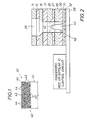
- Fig. 1 discloses an emitting tip, greatly enlarged, formed of a plurality of particles up to about 5.0 nanometers or less in maximum diameter.
- the microgun device 40 has a bottom conductor layer 41 made of the same material as particles 43 commingled in the cermet 42.
- the cermet is a mixture of conductive and insulative randomly distributed particles.
- the insulative particles are about 3.5 nanometer.
- the tip is preferably about 80 nanometers or less in radius and has a solid angle of 60° or less. Insulative and conductive particles are deposited by an ionic molecular process at cold temperature to produce the particle dimensions desired, about 3.5 nanometers.
- the conductive particles 43 are in ohmic contact with the insulative particles 44.
- the cermet 42 is biased in favor of conductive particles in ohmic contact with the support layer 41 and connects to a potential source through a conductor layer.
- the layer 41 is preferably formed of the same or a similar conducting material as the particles 43.
- the deposition builds up the tip with particles by dual vacuum particle emission with particle ballistics electrostatically directed and the surface is thereafter sputter etched to enhance insulator particle exposure.
- the conductive material has a higher sputter etching rate so it is partially removed to expose mostly insulative particles.
- the insulative particles 44 initiate the electron flow into space from the conic member.
- numeral 40 identifies the field emission device which has the upper cermet portion 42 above the conductive base portion 41.
- the base is an ohmic contact with a conductor 31 insulated from and upon an insulator (bottom) substrate 28.
- the emission device 40 is centered in an aperture 25. Proceeding upwardly from the bottom substrate 28, the next layer is an insulator layer 32. In turn, that supports the layer 31 of conductive material connected with the emitting microgun 40. Normally, the layer 28 is grounded while the layer 31 is connected to an acceleration voltage source in Fig. 4.
- the insulator layer 30 is preferably polyimide.
- the next layer 29 is the magnet layer deposition. It is placed just below the tip 42 to direct electrons away from the tip to initiate beam definition.
- the layer 29 is conductive material (discussed above) and also is part of the components forming a saddle field.
- the first anode 26 is a circle around the aperture 25.
- the circular conductive ring is sandwiched between adjacent insulative layers 27 and 17 typically of polyimides.
- the first anode layer 26 is typically between about 0.15 and 0.6 microns thick.
- the layer 27 is typically about 0.3 to about 1.0 microns thick. Thickness is a function of the electron optical characteristics desired.
- the layers 26, 27 and 29 extend to MOS or bipolar control circuitry formed simultaneously with the microgun.
- the cermet 42 extends about 0.15 micrometer above the bottom plane of the first anode 26.
- the cermet emitter ideally terminates approximately within the thickness of the anode 26.
- the anode 26 is undercut as shown in Fig. 2 because there is no compelling need to make this layer thicker.
- the structure of Fig. 2 is a sandwich of several deposited layers.
- the top layer 14 forms deflection bars above a polyimide insulator. Four bars deflect the beam where the bars are pairs of spaced, parallel bars.
- the deflection bars are above an insulative layer 15.
- the deflection bars (two pair) are parallel edges spaced about 1.7 micrometer apart to define X and Y deflection bars at right angles.
- the two pair in the layer 14 are identified in Fig. 4 as the deflection bars 20 and 21.
- the conductive layer 16 (sandwiched above and below by insulators) is a lense or focus layer for the emitted beam.
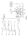
- FIG. 4 shows in exploded view the various anodes with the insulative material omitted. Also, the target is shown but the evacuated housing has been omitted for sake of clarity.
- the beam shaping layers are represented by rings or bars with conductor paths 51 to 58.
- the terminal 51 connects to the emitter 40.
- the magnet layer 29 connects to a selected voltage source.
- the anode 26 connects to the terminal 52.
- the anode 26 is positive, slightly less than 5 volts to initiate current emission.
- the wave form 51 is switched to ground while the wave form 52 is switched to approximately 5 volts positive to initiate emission.
- the other deflection plates 21 receive the potentials 53 and 58 stepped up by a bias and switched to opposite steps.
- the step up in the wave forms 53, 54, 55 and 58 forms an aperture lense focusing voltage, narrowing the beam.
- the various wave forms applied to the opposing focus electrodes are mirror images; this jointly deflects the beam in a controlled fashion and also narrows the beam.
- Focus , shaping and deflection are obtained by the step biases 60 applied to the wave forms 53, 54, 55 and 58.
- Beam modulation can be obtained by driving the anode 26 to cutoff, or to intermediate values to control the beam intensity. Beam focus or spot size is adjusted by the voltage applied to the layer 16. All the voltage wave forms shown in Fig. 3 can be obtained through MOS or bipoIar integrated circuits fabricated on a sideboard location. The control voltages applied to the deflector bars are in the millivolt range obtained by sideboard located integrated circuits.
Landscapes
- Cold Cathode And The Manufacture (AREA)
- Powder Metallurgy (AREA)
Priority Applications (4)
| Application Number | Priority Date | Filing Date | Title |
|---|---|---|---|
| US06/798,587 US4663559A (en) | 1982-09-17 | 1985-11-15 | Field emission device |
| DE8787303550T DE3782247D1 (de) | 1987-04-22 | 1987-04-22 | Feldemissionsvorrichtung. |
| EP87303550A EP0288616B1 (fr) | 1987-04-22 | 1987-04-22 | Dispositif d'émission de champ |
| AT87303550T ATE81565T1 (de) | 1987-04-22 | 1987-04-22 | Feldemissionsvorrichtung. |
Applications Claiming Priority (1)
| Application Number | Priority Date | Filing Date | Title |
|---|---|---|---|
| EP87303550A EP0288616B1 (fr) | 1987-04-22 | 1987-04-22 | Dispositif d'émission de champ |
Publications (2)
| Publication Number | Publication Date |
|---|---|
| EP0288616A1 true EP0288616A1 (fr) | 1988-11-02 |
| EP0288616B1 EP0288616B1 (fr) | 1992-10-14 |
Family
ID=8197873
Family Applications (1)
| Application Number | Title | Priority Date | Filing Date |
|---|---|---|---|
| EP87303550A Expired EP0288616B1 (fr) | 1982-09-17 | 1987-04-22 | Dispositif d'émission de champ |
Country Status (3)
| Country | Link |
|---|---|
| EP (1) | EP0288616B1 (fr) |
| AT (1) | ATE81565T1 (fr) |
| DE (1) | DE3782247D1 (fr) |
Cited By (4)
| Publication number | Priority date | Publication date | Assignee | Title |
|---|---|---|---|---|
| EP0483814A3 (en) * | 1990-10-30 | 1992-10-28 | Sony Corporation | Field emission type emitter and method of manufacturing thereof |
| EP0827176A3 (fr) * | 1996-08-16 | 2000-03-08 | Tektronix, Inc. | Revêtements conducteurs résistants à la pulvérisation à émission augmentée pour des électrodes cathodiques dans une structure d'adressage par plasma en courant continu |
| US6097139A (en) * | 1995-08-04 | 2000-08-01 | Printable Field Emitters Limited | Field electron emission materials and devices |
| EP1225613A4 (fr) * | 1999-10-12 | 2007-10-17 | Matsushita Electric Industrial Co Ltd | Dispositif emetteur d'electrons et source d'electrons le contenant, afficheur d'image a effet de champ, lampe fluorescente et leurs procedes de production |
Citations (5)
| Publication number | Priority date | Publication date | Assignee | Title |
|---|---|---|---|---|
| GB1226627A (fr) * | 1967-08-02 | 1971-03-31 | ||
| US4008412A (en) * | 1974-08-16 | 1977-02-15 | Hitachi, Ltd. | Thin-film field-emission electron source and a method for manufacturing the same |
| US4213192A (en) | 1979-01-15 | 1980-07-15 | Christensen Alton O Sr | Electron beam accessed read-write-erase random access memory |
| US4498952A (en) | 1982-09-17 | 1985-02-12 | Condesin, Inc. | Batch fabrication procedure for manufacture of arrays of field emitted electron beams with integral self-aligned optical lense in microguns |
| US4663559A (en) * | 1982-09-17 | 1987-05-05 | Christensen Alton O | Field emission device |
-
1987
- 1987-04-22 DE DE8787303550T patent/DE3782247D1/de not_active Expired - Lifetime
- 1987-04-22 EP EP87303550A patent/EP0288616B1/fr not_active Expired
- 1987-04-22 AT AT87303550T patent/ATE81565T1/de not_active IP Right Cessation
Patent Citations (5)
| Publication number | Priority date | Publication date | Assignee | Title |
|---|---|---|---|---|
| GB1226627A (fr) * | 1967-08-02 | 1971-03-31 | ||
| US4008412A (en) * | 1974-08-16 | 1977-02-15 | Hitachi, Ltd. | Thin-film field-emission electron source and a method for manufacturing the same |
| US4213192A (en) | 1979-01-15 | 1980-07-15 | Christensen Alton O Sr | Electron beam accessed read-write-erase random access memory |
| US4498952A (en) | 1982-09-17 | 1985-02-12 | Condesin, Inc. | Batch fabrication procedure for manufacture of arrays of field emitted electron beams with integral self-aligned optical lense in microguns |
| US4663559A (en) * | 1982-09-17 | 1987-05-05 | Christensen Alton O | Field emission device |
Non-Patent Citations (2)
| Title |
|---|
| O'REILLY, SOLID STATE ELECTRONICS, vol. 18, 1975, pages 965 |
| SIMMONS, JOURNAL OF PHYSICS, vol. 4, 1971, pages 641 |
Cited By (5)
| Publication number | Priority date | Publication date | Assignee | Title |
|---|---|---|---|---|
| EP0483814A3 (en) * | 1990-10-30 | 1992-10-28 | Sony Corporation | Field emission type emitter and method of manufacturing thereof |
| US5332627A (en) * | 1990-10-30 | 1994-07-26 | Sony Corporation | Field emission type emitter and a method of manufacturing thereof |
| US6097139A (en) * | 1995-08-04 | 2000-08-01 | Printable Field Emitters Limited | Field electron emission materials and devices |
| EP0827176A3 (fr) * | 1996-08-16 | 2000-03-08 | Tektronix, Inc. | Revêtements conducteurs résistants à la pulvérisation à émission augmentée pour des électrodes cathodiques dans une structure d'adressage par plasma en courant continu |
| EP1225613A4 (fr) * | 1999-10-12 | 2007-10-17 | Matsushita Electric Industrial Co Ltd | Dispositif emetteur d'electrons et source d'electrons le contenant, afficheur d'image a effet de champ, lampe fluorescente et leurs procedes de production |
Also Published As
| Publication number | Publication date |
|---|---|
| DE3782247D1 (de) | 1992-11-19 |
| ATE81565T1 (de) | 1992-10-15 |
| EP0288616B1 (fr) | 1992-10-14 |
Similar Documents
| Publication | Publication Date | Title |
|---|---|---|
| US4663559A (en) | Field emission device | |
| US5266155A (en) | Method for making a symmetrical layered thin film edge field-emitter-array | |
| US4682074A (en) | Electron-beam device and semiconductor device for use in such an electron-beam device | |
| US5030895A (en) | Field emitter array comparator | |
| US4574216A (en) | Cathode-ray tube and semiconductor device for use in such a cathode-ray tube | |
| JPH0145694B2 (fr) | ||
| JP3359677B2 (ja) | 荷電粒子ビームの形状制御を可能とする装置 | |
| US5734223A (en) | Field emission cold cathode having micro electrodes of different electron emission characteristics | |
| GB2374979A (en) | A field ionisation source | |
| US5656883A (en) | Field emission devices with improved field emission surfaces | |
| US5977696A (en) | Field emission electron gun capable of minimizing nonuniform influence of surrounding electric potential condition on electrons emitted from emitters | |
| US8450917B2 (en) | High-definition cathode ray tube and electron gun | |
| EP0288616B1 (fr) | Dispositif d'émission de champ | |
| US5786657A (en) | Field emission electron gun capable of minimizing nonuniform influence of surrounding electric potential condition on electrons emitted from emitters | |
| US5440579A (en) | Compact electron gun having a microdot electron source and a semiconductor laser using said gun for electronic pumping | |
| US4333035A (en) | Areal array of tubular electron sources | |
| KR20020038696A (ko) | 컴팩트한 전계 방출 전자총 및 집속 렌즈 | |
| US5990612A (en) | Field emitter array with cap material on anode electrode | |
| US6024618A (en) | Method of operating electron tube | |
| US4122369A (en) | Magnetic deflection apparatus positioned behind target | |
| US5723954A (en) | Pulsed hybrid field emitter | |
| JPS63274043A (ja) | 電界放射電子銃 | |
| US4196373A (en) | Electron optics apparatus | |
| JPH08106848A (ja) | 電子源およびそれを用いた陰極線管 | |
| JPH06243777A (ja) | 冷陰極 |
Legal Events
| Date | Code | Title | Description |
|---|---|---|---|
| PUAI | Public reference made under article 153(3) epc to a published international application that has entered the european phase |
Free format text: ORIGINAL CODE: 0009012 |
|
| AK | Designated contracting states |
Kind code of ref document: A1 Designated state(s): AT BE CH DE FR GB IT LI NL SE |
|
| 17P | Request for examination filed |
Effective date: 19890625 |
|
| 17Q | First examination report despatched |
Effective date: 19910131 |
|
| RAP3 | Party data changed (applicant data changed or rights of an application transferred) |
Owner name: CHRISTENSEN, ALTON OWEN |
|
| GRAA | (expected) grant |
Free format text: ORIGINAL CODE: 0009210 |
|
| AK | Designated contracting states |
Kind code of ref document: B1 Designated state(s): AT BE CH DE FR GB IT LI NL SE |
|
| PG25 | Lapsed in a contracting state [announced via postgrant information from national office to epo] |
Ref country code: SE Effective date: 19921014 Ref country code: NL Effective date: 19921014 Ref country code: BE Effective date: 19921014 Ref country code: DE Effective date: 19921014 Ref country code: AT Effective date: 19921014 Ref country code: IT Free format text: LAPSE BECAUSE OF FAILURE TO SUBMIT A TRANSLATION OF THE DESCRIPTION OR TO PAY THE FEE WITHIN THE PRESCRIBED TIME-LIMIT;WARNING: LAPSES OF ITALIAN PATENTS WITH EFFECTIVE DATE BEFORE 2007 MAY HAVE OCCURRED AT ANY TIME BEFORE 2007. THE CORRECT EFFECTIVE DATE MAY BE DIFFERENT FROM THE ONE RECORDED. Effective date: 19921014 |
|
| REF | Corresponds to: |
Ref document number: 81565 Country of ref document: AT Date of ref document: 19921015 Kind code of ref document: T |
|
| REF | Corresponds to: |
Ref document number: 3782247 Country of ref document: DE Date of ref document: 19921119 |
|
| ET | Fr: translation filed | ||
| NLV1 | Nl: lapsed or annulled due to failure to fulfill the requirements of art. 29p and 29m of the patents act | ||
| PLBE | No opposition filed within time limit |
Free format text: ORIGINAL CODE: 0009261 |
|
| STAA | Information on the status of an ep patent application or granted ep patent |
Free format text: STATUS: NO OPPOSITION FILED WITHIN TIME LIMIT |
|
| 26N | No opposition filed | ||
| PGFP | Annual fee paid to national office [announced via postgrant information from national office to epo] |
Ref country code: CH Payment date: 19950425 Year of fee payment: 9 |
|
| PG25 | Lapsed in a contracting state [announced via postgrant information from national office to epo] |
Ref country code: LI Effective date: 19960430 Ref country code: CH Effective date: 19960430 |
|
| REG | Reference to a national code |
Ref country code: CH Ref legal event code: PL |
|
| PGFP | Annual fee paid to national office [announced via postgrant information from national office to epo] |
Ref country code: GB Payment date: 19980415 Year of fee payment: 12 |
|
| PGFP | Annual fee paid to national office [announced via postgrant information from national office to epo] |
Ref country code: FR Payment date: 19980427 Year of fee payment: 12 |
|
| PG25 | Lapsed in a contracting state [announced via postgrant information from national office to epo] |
Ref country code: GB Free format text: LAPSE BECAUSE OF NON-PAYMENT OF DUE FEES Effective date: 19990422 |
|
| GBPC | Gb: european patent ceased through non-payment of renewal fee |
Effective date: 19990422 |
|
| PG25 | Lapsed in a contracting state [announced via postgrant information from national office to epo] |
Ref country code: FR Free format text: LAPSE BECAUSE OF NON-PAYMENT OF DUE FEES Effective date: 19991231 |
|
| REG | Reference to a national code |
Ref country code: FR Ref legal event code: ST |