EP0288765B1 - Capteur magnétorésistif à film antiferromagnétique de phase mixte - Google Patents
Capteur magnétorésistif à film antiferromagnétique de phase mixte Download PDFInfo
- Publication number
- EP0288765B1 EP0288765B1 EP88105076A EP88105076A EP0288765B1 EP 0288765 B1 EP0288765 B1 EP 0288765B1 EP 88105076 A EP88105076 A EP 88105076A EP 88105076 A EP88105076 A EP 88105076A EP 0288765 B1 EP0288765 B1 EP 0288765B1
- Authority
- EP
- European Patent Office
- Prior art keywords
- femn
- layer
- sensor
- phase
- alpha
- Prior art date
- Legal status (The legal status is an assumption and is not a legal conclusion. Google has not performed a legal analysis and makes no representation as to the accuracy of the status listed.)
- Expired - Lifetime
Links
- 230000005290 antiferromagnetic effect Effects 0.000 title description 13
- 229910015136 FeMn Inorganic materials 0.000 claims description 46
- 229910001030 Iron–nickel alloy Inorganic materials 0.000 claims description 15
- 239000000758 substrate Substances 0.000 claims description 13
- 239000011521 glass Substances 0.000 claims description 6
- 229910045601 alloy Inorganic materials 0.000 claims description 5
- 239000000956 alloy Substances 0.000 claims description 5
- 239000002885 antiferromagnetic material Substances 0.000 claims description 5
- 239000003302 ferromagnetic material Substances 0.000 claims description 3
- 230000001939 inductive effect Effects 0.000 claims description 2
- 239000010408 film Substances 0.000 description 20
- 230000005291 magnetic effect Effects 0.000 description 8
- 230000005294 ferromagnetic effect Effects 0.000 description 7
- 238000004544 sputter deposition Methods 0.000 description 6
- 230000000694 effects Effects 0.000 description 5
- 238000002441 X-ray diffraction Methods 0.000 description 4
- 230000008878 coupling Effects 0.000 description 4
- 238000010168 coupling process Methods 0.000 description 4
- 238000005859 coupling reaction Methods 0.000 description 4
- 238000000151 deposition Methods 0.000 description 4
- 239000010949 copper Substances 0.000 description 3
- 230000008021 deposition Effects 0.000 description 3
- 230000001965 increasing effect Effects 0.000 description 3
- 230000005381 magnetic domain Effects 0.000 description 3
- XKRFYHLGVUSROY-UHFFFAOYSA-N Argon Chemical compound [Ar] XKRFYHLGVUSROY-UHFFFAOYSA-N 0.000 description 2
- 230000005330 Barkhausen effect Effects 0.000 description 2
- 229910000914 Mn alloy Inorganic materials 0.000 description 2
- 239000011572 manganese Substances 0.000 description 2
- 239000000463 material Substances 0.000 description 2
- 229910052715 tantalum Inorganic materials 0.000 description 2
- GUVRBAGPIYLISA-UHFFFAOYSA-N tantalum atom Chemical compound [Ta] GUVRBAGPIYLISA-UHFFFAOYSA-N 0.000 description 2
- 238000005382 thermal cycling Methods 0.000 description 2
- 239000010409 thin film Substances 0.000 description 2
- RYGMFSIKBFXOCR-UHFFFAOYSA-N Copper Chemical compound [Cu] RYGMFSIKBFXOCR-UHFFFAOYSA-N 0.000 description 1
- PWHULOQIROXLJO-UHFFFAOYSA-N Manganese Chemical compound [Mn] PWHULOQIROXLJO-UHFFFAOYSA-N 0.000 description 1
- 229910052786 argon Inorganic materials 0.000 description 1
- 239000004020 conductor Substances 0.000 description 1
- 229910052802 copper Inorganic materials 0.000 description 1
- DALUDRGQOYMVLD-UHFFFAOYSA-N iron manganese Chemical compound [Mn].[Fe] DALUDRGQOYMVLD-UHFFFAOYSA-N 0.000 description 1
- UGKDIUIOSMUOAW-UHFFFAOYSA-N iron nickel Chemical compound [Fe].[Ni] UGKDIUIOSMUOAW-UHFFFAOYSA-N 0.000 description 1
- 238000012886 linear function Methods 0.000 description 1
- 229910052748 manganese Inorganic materials 0.000 description 1
- 229910052751 metal Inorganic materials 0.000 description 1
- 239000002184 metal Substances 0.000 description 1
- 150000002739 metals Chemical class 0.000 description 1
- 238000000034 method Methods 0.000 description 1
- 239000000203 mixture Substances 0.000 description 1
- 229910052750 molybdenum Inorganic materials 0.000 description 1
- 229910052758 niobium Inorganic materials 0.000 description 1
- 125000006850 spacer group Chemical group 0.000 description 1
- 229910052721 tungsten Inorganic materials 0.000 description 1
Images

Classifications
-
- G—PHYSICS
- G11—INFORMATION STORAGE
- G11B—INFORMATION STORAGE BASED ON RELATIVE MOVEMENT BETWEEN RECORD CARRIER AND TRANSDUCER
- G11B5/00—Recording by magnetisation or demagnetisation of a record carrier; Reproducing by magnetic means; Record carriers therefor
- G11B5/127—Structure or manufacture of heads, e.g. inductive
- G11B5/33—Structure or manufacture of flux-sensitive heads, i.e. for reproduction only; Combination of such heads with means for recording or erasing only
- G11B5/39—Structure or manufacture of flux-sensitive heads, i.e. for reproduction only; Combination of such heads with means for recording or erasing only using magneto-resistive devices or effects
- G11B5/3903—Structure or manufacture of flux-sensitive heads, i.e. for reproduction only; Combination of such heads with means for recording or erasing only using magneto-resistive devices or effects using magnetic thin film layers or their effects, the films being part of integrated structures
Definitions
- This invention relates to magnetoresistive (MR) read sensors, and in particular to a MR read sensor in which an improved antiferromagnetic film provides a longitudinal bias field in the ferromagnetic MR film of the sensor.
- MR magnetoresistive
- a MR sensor for reading information signals from a magnetic recording medium is described in US-A-4,103,315 by Hempstead, et al. disclosing the features of the preamble of claim 1.
- the patent describes a MR read sensor which utilizes antiferromagnetic ferromagnetic exchange coupling to produce a uniform longitudinal bias in the MR layer of the sensor.
- EP-A-0216062 is directed to such a MR sensor, but describes an FeMn antiferromagnetic layer which is divided into separate end portions for providing an exchange bias primarily in the adjacent end portions of the MR layer.
- the exchange coupling between the antiferromagnetic and ferromagnetic layers creates a single domain state in the ferromagnetic layer and thereby suppresses the so-called Barkhausen noise associated with domain activity. For this reason it is desirable to maximize the exchange bias effect in the MR layer.
- the materials suggested by the US-A-4103315 are nickel-iron (NiFe) as the ferromagnetic MR layer and a face-centered-cubic (FCC) phase (gamma phase) of manganese (Mn) alloy as the antiferromagnetic layer.
- NiFe nickel-iron
- FCC face-centered-cubic
- Mn manganese
- FeMn iron-manganese
- the present invention provides a magnetoresistive sensor of the type having a layer of antiferromagnetic material in direct contact with a magnetoresistive layer of ferromagnetic material for inducing a longitudinal exchange bias field in the magnetoresistive layer, the antiferromagnetic material comprising a FeMn alloy including FeMn in both the gamma phase and the alpha phase, characterised in that: the amount of FeMn in the alpha phase exceeds the amount of FeMn in the gamma phase.
- the improved antiferromagnetic layer composition substantially increases the exchange bias effect in the MR sensor.
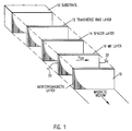
- a typical thin film MR sensor comprises a substrate 10, a transverse bias layer 12, a spacer layer 14, a MR layer 16 and an antiferromagnetic layer 18.
- the MR layer 16 which is formed of ferromagnetic material such as Ni80Fe20, is attached to electrical conductors 20 and provides an output current.
- the output current from MR layer 16 is a signal which enables a separate sensing circuit to determine resistance changes in the MR layer.
- the resistance changes are a function of changes in the magnetic fields intercepted by MR layer 16 from recorded data on the magnetic storage medium.
- an antiferromagnetic layer is formed on MR layer 16.
- the antiferromagnetic layer which in the prior art may be the gamma phase of Mn alloys, creates an interface exchange coupling with the ferromagnetic MR layer 16. This results in a longitudinal exchange bias field (H UA ) in MR layer 16 and creates a single magnetic domain state in MR layer 16.
- H UA longitudinal exchange bias field
- the existence of a single magnetic domain state in MR layer 16 is essential to suppress Barkhausen noise which is associated with MR materials which exhibit multiple magnetic domain states.
- the transverse bias layer 12 provides a magnetic field oriented generally perpendicular to the medium so as to slightly bias the magnetic field in MR layer 16 in a direction non-parallel to the medium. This transverse bias maintains the MR layer 16 in a linear response mode such that the current output is essentially a linear function of the resistance changes.
- the transverse bias can be provided by shunt biasing, soft film biasing, or permanent magnet biasing.
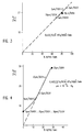
- film structures were formed by depositing films of FeMn under various sputtering conditions on NiFe layers formed on different substrates. An X-ray diffraction analysis was then performed on these FeMn films. A comparison of the relative values of the diffraction peaks with the known peaks for the alpha and gamma phases yielded the relative percentages of the two phases present in the FeMn film. A magnetic hystersis loop was then computed for the film structures by use of a vibrating scanning magnetometer to determine the loop shift or exchange bias (H UA ). The magnitude of H UA was then plotted as a function of the relative amounts of the alpha and gamma phases of FeMn.
- H UA loop shift or exchange bias
- Figs. 2A and 2B The calculated X-ray diffraction patterns for phases of pure alpha and pure gamma FeMn are shown in Figs. 2A and 2B. Each of the peaks corresponds to reflection from a particular plane in the crystalline structure, as identified in Figs. 2A and 2B. Thus, it is possible to determine the presence of the FeMn phases in a particular film from an X-ray diffraction scan by comparing the location of the measured peaks with the location of the known peaks.
- the relative magnitudes of the diffraction peaks corresponding to the respective FeMn phases were measured for two sets of FeMn films.
- the first set of FeMn films was deposited on a 40 nm NiFe layer formed directly on a glass substrate, and the second set of FeMn films was deposited on a 40 nm NiFe layer formed on a hexagonal-close-packed (HCP) tantalum (the beta phase of Ta) underlayer on a glass substrate.
- HCP hexagonal-close-packed
- the exchange bias was measured for these films and plotted as a function of percent alpha FeMn in the FeMn film. This data is shown in Figs. 3 and 4, wherein each data point is identified by the specific sputtering conditions of target voltage and argon pressure.
- the data shown in Figs. 3 and 4 indicate that the exchange bias is increased by the amount of alpha FeMn present in the antiferromagnetic layer.
- the amount of alpha FeMn present strongly depends upon the substrate and the sputtering conditions.
- the strength of the exchange bias is a function not only of the substrate on which the NiFe layer is formed, but also the sputtering conditions.
- H UA is increased at lower target voltages, which corresponds to low deposition rates, and at higher sputtering pressures.
- the exchange bias, H UA varies from 560 A/m to 2320 A/m with the sputtering pressures and target voltages.
- Deposition of NiFe/FeMn on glass or other nonmetallic substrates reduces the dependence of H UA in deposition power and pressure (Fig. 3) and produces large amounts of the alpha FeMn phase.
- the presence of a BCC phase of Ta as an underlayer (or other BCC metals such as Mo, W, and Nb) tends to increase the amount of the alpha FeMn phase.
- alpha FeMn is the stable phase of the FeMn alloy
- a MR sensor formed with an antiferromagnetic FeMn layer containing alpha FeMn as the dominant phase exhibits exchange bias properties that are unchanged after thermal cycling from room temperature to a process temperature of approximately 260°C over a 20 hour period.
- FeMn films which contain little or no alpha FeMn have been observed to produce MR sensors with exchange properties that degrade with such repeated thermal cycling.
Landscapes
- Engineering & Computer Science (AREA)
- Manufacturing & Machinery (AREA)
- Magnetic Heads (AREA)
- Hall/Mr Elements (AREA)
- Measuring Magnetic Variables (AREA)
- Thin Magnetic Films (AREA)
Claims (5)
- Capteur magnétorésistif du type ayant une couche de matériau antiferromagnétique (18) en contact direct avec une couche magnétorésistive de matériau ferromagnétique (16) pour induire un champ de polarisation d'échange longitudinal (HUA) dans la couche magnétorésistive (16), le matériau antiferromagnétique comprenant un alliage FeMn comportant FeMn aussi bien en phase alpha qu'en phase gamma, caractérisé en ce que :
la quantité de FeMn en phase alpha est plus grande que la quantité de FeMn en phase gamma. - Capteur tel que revendiqué dans la revendication 1, comprenant en outre un moyen (12) pour produire un champ de polarisation transversale dans ladite couche magnétorésistive (16).
- Capteur tel que revendiqué dans la revendication 2, dans lequel la couche magnétorésistive est un alliage comprenant NiFe.
- Capteur tel que revendiqué dans une quelconque des revendications précédentes, dans lequel la couche magnétorésistive est déposée sur un substrat non métallique.
- Capteur tel que revendiqué dans la revendication 4, dans lequel ledit substrat non métallique est un substrat de verre.
Applications Claiming Priority (2)
| Application Number | Priority Date | Filing Date | Title |
|---|---|---|---|
| US43674 | 1987-04-28 | ||
| US07/043,674 US4782413A (en) | 1987-04-28 | 1987-04-28 | Magnetoresistive sensor with mixed phase antiferromagnetic film |
Publications (3)
| Publication Number | Publication Date |
|---|---|
| EP0288765A2 EP0288765A2 (fr) | 1988-11-02 |
| EP0288765A3 EP0288765A3 (en) | 1990-11-07 |
| EP0288765B1 true EP0288765B1 (fr) | 1993-08-04 |
Family
ID=21928315
Family Applications (1)
| Application Number | Title | Priority Date | Filing Date |
|---|---|---|---|
| EP88105076A Expired - Lifetime EP0288765B1 (fr) | 1987-04-28 | 1988-03-29 | Capteur magnétorésistif à film antiferromagnétique de phase mixte |
Country Status (4)
| Country | Link |
|---|---|
| US (1) | US4782413A (fr) |
| EP (1) | EP0288765B1 (fr) |
| JP (1) | JPH0636444B2 (fr) |
| DE (1) | DE3882786T2 (fr) |
Families Citing this family (15)
| Publication number | Priority date | Publication date | Assignee | Title |
|---|---|---|---|---|
| US5001586A (en) * | 1989-08-01 | 1991-03-19 | International Business Machines Corporation | Very low noise magnetoresistive sensor for high density media applications |
| US5014147A (en) * | 1989-10-31 | 1991-05-07 | International Business Machines Corporation | Magnetoresistive sensor with improved antiferromagnetic film |
| US5043693A (en) * | 1990-08-13 | 1991-08-27 | The United States Of America As Represented By The Secretary Of The Navy | Heterogeneous magnetoresistive layer |
| MY108176A (en) * | 1991-02-08 | 1996-08-30 | Hitachi Global Storage Tech Netherlands B V | Magnetoresistive sensor based on oscillations in the magnetoresistance |
| EP0570883B1 (fr) * | 1992-05-18 | 1998-01-21 | Nec Corporation | Elément magnétorésistif |
| US5315468A (en) * | 1992-07-28 | 1994-05-24 | International Business Machines Corporation | Magnetoresistive sensor having antiferromagnetic layer for exchange bias |
| US5475550A (en) * | 1992-08-25 | 1995-12-12 | Seagate Technology, Inc. | Enhanced cross-talk suppression in magnetoresistive sensors |
| US5440233A (en) * | 1993-04-30 | 1995-08-08 | International Business Machines Corporation | Atomic layered materials and temperature control for giant magnetoresistive sensor |
| US5668523A (en) * | 1993-12-29 | 1997-09-16 | International Business Machines Corporation | Magnetoresistive sensor employing an exchange-bias enhancing layer |
| US5666247A (en) * | 1994-02-04 | 1997-09-09 | Seagate Technology, Inc. | No-field, low power FeMn deposition giving high exchange films |
| JP3651619B2 (ja) * | 1995-06-29 | 2005-05-25 | 富士通株式会社 | 磁気抵抗効果型トランスデューサ及び磁気記録装置 |
| JP3990751B2 (ja) * | 1995-07-25 | 2007-10-17 | 株式会社日立グローバルストレージテクノロジーズ | 磁気抵抗効果型磁気ヘッド及び磁気記録再生装置 |
| US6055135A (en) * | 1996-03-25 | 2000-04-25 | Alps Electric Co., Ltd. | Exchange coupling thin film and magnetoresistive element comprising the same |
| JP3833362B2 (ja) * | 1997-10-01 | 2006-10-11 | 富士通株式会社 | 磁気抵抗効果型ヘッド |
| US6650512B1 (en) | 2000-03-21 | 2003-11-18 | International Business Machines Corporation | GMR coefficient enhancement of a spin valve structure |
Family Cites Families (4)
| Publication number | Priority date | Publication date | Assignee | Title |
|---|---|---|---|---|
| US3840898A (en) * | 1972-12-29 | 1974-10-08 | Ibm | Self-biased magnetoresistive sensor |
| US3887944A (en) * | 1973-06-29 | 1975-06-03 | Ibm | Method for eliminating part of magnetic crosstalk in magnetoresistive sensors |
| US4103315A (en) * | 1977-06-24 | 1978-07-25 | International Business Machines Corporation | Antiferromagnetic-ferromagnetic exchange bias films |
| US4663685A (en) * | 1985-08-15 | 1987-05-05 | International Business Machines | Magnetoresistive read transducer having patterned longitudinal bias |
-
1987
- 1987-04-28 US US07/043,674 patent/US4782413A/en not_active Expired - Fee Related
-
1988
- 1988-03-17 JP JP63062112A patent/JPH0636444B2/ja not_active Expired - Lifetime
- 1988-03-29 DE DE88105076T patent/DE3882786T2/de not_active Expired - Fee Related
- 1988-03-29 EP EP88105076A patent/EP0288765B1/fr not_active Expired - Lifetime
Also Published As
| Publication number | Publication date |
|---|---|
| JPH0636444B2 (ja) | 1994-05-11 |
| EP0288765A2 (fr) | 1988-11-02 |
| US4782413A (en) | 1988-11-01 |
| DE3882786D1 (de) | 1993-09-09 |
| JPS63273373A (ja) | 1988-11-10 |
| DE3882786T2 (de) | 1994-03-17 |
| EP0288765A3 (en) | 1990-11-07 |
Similar Documents
| Publication | Publication Date | Title |
|---|---|---|
| EP0288766B1 (fr) | Capteur magnétorésistif à film antiferromagnétique | |
| US5014147A (en) | Magnetoresistive sensor with improved antiferromagnetic film | |
| EP0681338B1 (fr) | Dispositif à magnétorésistance et tête à effet de magnétorésistance, dispositif de mémoire et amplificateur utilisant ce dispositif | |
| US5989690A (en) | Magnetoresistance effect film, a method of manufacturing the same, and magnetoresistance effect device | |
| US4825325A (en) | Magnetoresistive read transducer assembly | |
| EP0701142B1 (fr) | Film à effet magnétorésistif et procédé de fabrication | |
| EP0674327B1 (fr) | Film à soupape de spin | |
| JP3088478B2 (ja) | 磁気抵抗効果素子 | |
| US6023395A (en) | Magnetic tunnel junction magnetoresistive sensor with in-stack biasing | |
| EP0751499B1 (fr) | Capteur magnétorésistif | |
| EP0334480B1 (fr) | Un transducteur de lecture magnetorésistif et une méthode pour le fabriquer | |
| EP0288765B1 (fr) | Capteur magnétorésistif à film antiferromagnétique de phase mixte | |
| US5552949A (en) | Magnetoresistance effect element with improved antiferromagnetic layer | |
| EP0724301B1 (fr) | Film à effet magnétorésistif | |
| US5764445A (en) | Exchange biased magnetoresistive transducer | |
| US5843589A (en) | Magnetic layered material, and magnetic sensor and magnetic storage/read system based thereon | |
| GB2398920A (en) | Spin valve magnetoresistive element | |
| US5258884A (en) | Magnetoresistive read transducer containing a titanium and tungsten alloy spacer layer | |
| EP0624868B1 (fr) | Eléments magnéto-résistifs et procédé de fabrication | |
| KR100266518B1 (ko) | 자기저항효과막및그의제조방법 | |
| US5668687A (en) | Magnetoresistive sensor employing an exchange-bias enhancing layer with a variable-composition transition region | |
| Ueno et al. | Magnetic properties of ion‐beam sputter deposited NiFe ultrathin films | |
| JP3217625B2 (ja) | 磁気抵抗効果型ヘッド | |
| US6001430A (en) | Magnetoresistance effect film and production process thereof | |
| JP3021785B2 (ja) | 磁気抵抗効果材料およびその製造方法 |
Legal Events
| Date | Code | Title | Description |
|---|---|---|---|
| PUAI | Public reference made under article 153(3) epc to a published international application that has entered the european phase |
Free format text: ORIGINAL CODE: 0009012 |
|
| AK | Designated contracting states |
Kind code of ref document: A2 Designated state(s): DE FR GB |
|
| 17P | Request for examination filed |
Effective date: 19890222 |
|
| PUAL | Search report despatched |
Free format text: ORIGINAL CODE: 0009013 |
|
| AK | Designated contracting states |
Kind code of ref document: A3 Designated state(s): DE FR GB |
|
| 17Q | First examination report despatched |
Effective date: 19911218 |
|
| GRAA | (expected) grant |
Free format text: ORIGINAL CODE: 0009210 |
|
| AK | Designated contracting states |
Kind code of ref document: B1 Designated state(s): DE FR GB |
|
| REF | Corresponds to: |
Ref document number: 3882786 Country of ref document: DE Date of ref document: 19930909 |
|
| ET | Fr: translation filed | ||
| PLBE | No opposition filed within time limit |
Free format text: ORIGINAL CODE: 0009261 |
|
| STAA | Information on the status of an ep patent application or granted ep patent |
Free format text: STATUS: NO OPPOSITION FILED WITHIN TIME LIMIT |
|
| 26N | No opposition filed | ||
| PGFP | Annual fee paid to national office [announced via postgrant information from national office to epo] |
Ref country code: GB Payment date: 19950227 Year of fee payment: 8 |
|
| PGFP | Annual fee paid to national office [announced via postgrant information from national office to epo] |
Ref country code: FR Payment date: 19950228 Year of fee payment: 8 |
|
| PGFP | Annual fee paid to national office [announced via postgrant information from national office to epo] |
Ref country code: DE Payment date: 19950330 Year of fee payment: 8 |
|
| PG25 | Lapsed in a contracting state [announced via postgrant information from national office to epo] |
Ref country code: GB Effective date: 19960329 |
|
| GBPC | Gb: european patent ceased through non-payment of renewal fee |
Effective date: 19960329 |
|
| PG25 | Lapsed in a contracting state [announced via postgrant information from national office to epo] |
Ref country code: FR Effective date: 19961129 |
|
| PG25 | Lapsed in a contracting state [announced via postgrant information from national office to epo] |
Ref country code: DE Effective date: 19961203 |
|
| REG | Reference to a national code |
Ref country code: FR Ref legal event code: ST |