EP0289044A2 - Détecteur d'images couleur et son procédé de fabrication - Google Patents
Détecteur d'images couleur et son procédé de fabrication Download PDFInfo
- Publication number
- EP0289044A2 EP0289044A2 EP88106914A EP88106914A EP0289044A2 EP 0289044 A2 EP0289044 A2 EP 0289044A2 EP 88106914 A EP88106914 A EP 88106914A EP 88106914 A EP88106914 A EP 88106914A EP 0289044 A2 EP0289044 A2 EP 0289044A2
- Authority
- EP
- European Patent Office
- Prior art keywords
- color
- image sensor
- color filters
- picture cell
- covering
- Prior art date
- Legal status (The legal status is an assumption and is not a legal conclusion. Google has not performed a legal analysis and makes no representation as to the accuracy of the status listed.)
- Granted
Links
Images




Classifications
-
- H—ELECTRICITY
- H10—SEMICONDUCTOR DEVICES; ELECTRIC SOLID-STATE DEVICES NOT OTHERWISE PROVIDED FOR
- H10F—INORGANIC SEMICONDUCTOR DEVICES SENSITIVE TO INFRARED RADIATION, LIGHT, ELECTROMAGNETIC RADIATION OF SHORTER WAVELENGTH OR CORPUSCULAR RADIATION
- H10F77/00—Constructional details of devices covered by this subclass
- H10F77/30—Coatings
- H10F77/306—Coatings for devices having potential barriers
- H10F77/331—Coatings for devices having potential barriers for filtering or shielding light, e.g. multicolour filters for photodetectors
-
- H—ELECTRICITY
- H10—SEMICONDUCTOR DEVICES; ELECTRIC SOLID-STATE DEVICES NOT OTHERWISE PROVIDED FOR
- H10F—INORGANIC SEMICONDUCTOR DEVICES SENSITIVE TO INFRARED RADIATION, LIGHT, ELECTROMAGNETIC RADIATION OF SHORTER WAVELENGTH OR CORPUSCULAR RADIATION
- H10F39/00—Integrated devices, or assemblies of multiple devices, comprising at least one element covered by group H10F30/00, e.g. radiation detectors comprising photodiode arrays
- H10F39/10—Integrated devices
- H10F39/12—Image sensors
- H10F39/15—Charge-coupled device [CCD] image sensors
- H10F39/156—CCD or CID colour image sensors
Definitions
- the present invention relates to a solid-state color image sensor and a method of manufacturing the same, for use particularly with an electronic still camera.
- a solid-state color image sensor has photoelectric conversion cells arranged in a matrix configuration and associated color filters to pick up color signals.
- An image sensor used in the field integration mode is constructed such that color filters of magenta (Mg), cyan (Cy), green (G) and cyan are disposed in this order in the 1st column (1), color filters of green, yellow (Ye), magenta and yellow are disposed in this order in the 2nd column (2), and the two columns with such color filter arrangement are alternately disposed over the whole area of the sensor.
- a mixed column readout method is used whereby at the 1st field defining a certain scan line, both the rows (a) and (b) are read out together to obtain a sum of Mg+Cy signal and G+Ye signal, and at the 2nd field defining the next scan line, both the rows (b) and (c) are read out together to obtain a sum of Cy+G signal and Ye+Mg signal.
- Each photoelectric conversion area is formed in alignment with the center of each color filter.
- the green (G) filter is obtained by superposing the yellow and cyan filters.
- the image resolution thereof is dependent on the size of picture cell so that its vertical resolution is not sufficient for being used by electronic still cameras which require a high resolution.
- Fig. 1B shows the arrangement of color filters used in the frame integration mode.
- Each color filter provided for each picture cell is constructed of two color filters each being a half size as that used in the field integration mode.
- an Mg/Cy filter and a G/Ye filter are alternately disposed, and at the (b) line a Cy/G filter and an Ye/Mg filter are alternately disposed.
- each frame is read in unit of one line such that at the row (a) of the 1st frame, signals Mg+Cy and G+Ye are obtained and at the row (b) of the 2nd frame, signals Cy+G and Ye+Mg are obtained.
- the material such as casein of a color filter used in the frame integration mode has a poor resolution and hence poor alignment precision at the joint between two halves of the color filter.
- the obtained color filter may therefore operate stronger at one color than at the other color so that flicker noises are superposed on color difference signals.
- a solid-state color image sensor of the type having color filters of a plurality of different colors formed above a plurality of photosensitive picture cells on a semiconductor substrate surface comprises color filters of first to third different colors including magenta, yellow and cyan; wherein color filters of said first color are used for color filters each covering the entire area of a first type picture cell, and for color filters each covering a predetermined ratio of the entire area of a second or third type picture cell; color filters of said second color are used for color filters each covering the entire area of said second type picture cell, and for color filters each covering a predetermined ratio of the entire area of a fourth type picture cell; and color filters of said third color are used for color filters each covering the entire area of said third or fourth type picture cell.
- the color filters covering predetermined ratios of the entire areas of picture cells are preferably formed collectively in a stripe shape.
- the color filters covering predetermined ratios of the entire areas of picture cells may be formed as the upper layer on the lower color filter layer covering the entire areas of picture cells.
- a method of manufacturing a solid-state color image sensor of the type forming color filters of a plurality of different colors above a plurality of photosensitive picture cells disposed in a matrix configuration on a semiconductor substrate surface comprises the following steps (a) to (e) which are carried out sequentially in an optional order and may or may not include those steps carried out at the same time:
- each half area of the first to fourth type picture cell is covered with a color filter of one of the colors including magenta, yellow and cyan, and the other half is covered with a color filter of another of the colors including magenta, yellow and cyan. Therefore, it becomes possible to read image signals either at the field integration mode or at the frame integration mode, by properly selecting the positional arrangement of the first to fourth type picture cells in the image sensor. Further, since each picture cell is covered with two different color filters, the vertical resolution of color signals can be improved two times as good as that of an image sensor using one color filter per picture cell. Furthermore, use of the complementary color filters assures the sensitivity of the sensor without lowering it considerably, and use of cyan, yellow and magenta three colors retains a good color reproductivity.
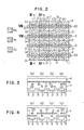
- Fig. 2 is a partial plan view of an embodiment of a solid-state color image sensor according to the present invention
- Figs. 3 and 4 are cross sectional views showing the internal construction of the image sensor, respectively taken along lines III-III and IV-IV of Fig. 2.
- the solid-state color image sensor is constructed as having color filters of a plurality of different colors formed on a solid-state image sensor main body or semiconductor substrate with a plurality of photosensitive picture cells.
- the semiconductor substrate 1 has photosensitive picture cells 2, 2, ... such as photo diodes below the surface thereof.
- Each of the photosensitive picture cells 2, 2, ... is indicated by a broken-line rectangular in Fig. 2.
- Aluminum light shielding films 3, 3, .... are formed above the surface of the semiconductor substrate 1, the opening of the light shielding film 3 corresponding in position to the photosensitive picture cell.
- a transparent layer 4 is formed within which Ye, Cy and Mg color filters are sequentially formed, the colors being complementary colors of blue (B), red (R) and green (G).
- the colors being complementary colors of blue (B), red (R) and green (G).
- rectangular Ye color filters 11 are formed at the 2nd and 4th columns at the row (a) and at the 2nd and 4th columns at the row (d) to cover the whole areas c and hence the entire areas of respective picture cells 2 within the areas c .
- Ye color filters 12 in a stripe shape having a width of a predetermined ratio, e.g. half, the picture cell width are formed at the rows (b) and (c) as shown in Figs.
- each Ye color filter 12 traversing substantially at the center of each picture cell 2 and covering a predetermined ratio, e.g. a half of the entire area of each picture cell within the areas b and d .
- rectangular Cy color filters 21 are formed at the 2nd and 4th columns at the rows (b) and (c) to cover the whole areas d and hence the entire areas of respective picture cells 2 within the areas d .
- Cy color filters 22 in a stripe shape having a width half the picture cell width are formed at the rows (a) and (d) as shown in Figs. 2 to 4, each Cy color filter 22 traversing substantially at the center of each picture cell 2 and covering a half of the entire area of each picture cell within the areas a and c .
- rectangular Mg color filters 31 are formed at the 1st and 3rd columns to cover the whole areas a and b and hence the entire areas of respective picture cells within the areas a and b .
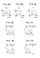
- Figs. 5A to 5C show the spectrum transmittance characteristics of Mg, Cy and Ye color filters of this invention, each of which shows an output of each picture cell 2 assuming that only one of Mg, Ye and Cy color filters covers the entire area of the picture cells shown in Fig. 2.
- the Mg, Cy and Ye color filters are used which have been subjected to the coloring to obtain the characteristics shown in Figs. 5A to 5°C, respectively.
- the coloring density of Mg in particular has a transmittance of 40 to 60% at a wavelength of 550 nm.
- Figs. 6A to 6C are schematic diagrams showing the characteristics of Figs. 5A to 5C, respectively.
- the transmittance characteristics at the areas a to d of the solid-state color image sensor with the color filters having the characteristics of Figs. 6A to 6C (5A to 5C) and constructed as shown in Figs. 2 to 4 are shown in Figs. 7A to 7D.
- a half of the entire area of the photosensitive picture cell 2 is covered with only Mg color filter 31 and the remaining half of the picture cell is covered with both Mg color filter 31 and Cy color filter 22. Therefore, the picture cell 2 at the area a can be considered as being covered by a color filter [Mg/2 + (Mg + Cy)/2].
- FIG. 7A An output from the picture cell 2 at the area a therefore becomes as shown in Fig. 7A which shows that the R component was cut by Cy as indicated by a broken line.
- picture cells 2 at areas b to d are covered with color filters [Mg/2 + (Mg + Ye)/2], [Ye/2 + (Ye + Cy)/2] - [Ye/2 + G/2)] and [Cy/2 + (Ye + Cy)/2] - [Cy/2 + G/2], respectively.
- the outputs from the picture cells 2 at the areas b to d are shown in Figs. 7B to 7D.
- An output shown in Fig. 7B indicates that the B component of Mg was eliminated by Ye
- an output shown in Fig. 7C indicates that the R component of Ye was eliminated by Cy
- an output shown in Fig. 7D indicates that the B component of Cy was cut by Ye.
- the vertical resolution of color signals can be obtained which is two times as high as the conventional solid-state color image sensor.
- Such high resolution is particularly suitable for those solid-state image sensors of electronic still cameras which require a high vertical color signal resolution.
- complementary type color filters are used, a high sensitivity can be maintained.
- use of Cy, Ye and Mg three colors enables a good color reproductivity in the line sequential color difference signal method.
- the stripe filter with a half of the picture cell width can be formed within the area of the picture cell without failure so that a slight displacement of patterns hardly causes a change in ratio of areas occupied by two different filters and hence a change in spectrum transmittance, thus achieving a stable characteristic.
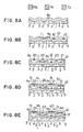
- Figs. 8A to 8E are cross sectional views each showing a different process of an embodiment of a manufacturing method of the solid-state color image sensor. Each cross section showing the process corresponds to that taken along line VIII(E)-VIII(E) shown in Fig. 2. The embodiment of the method of manufacturing a solid-state color image sensor will be described with reference to Figs. 8A to 8E.
- reference numerals 1 to 3 denote the same elements described previously. Namely, reference numeral 1 denotes a semiconductor substrate, 2 a photosensitive picture cell, and 3 an aluminum lightshielding film.
- a transparent layer (base layer) 4a of acrylic resin type is formed on the solid-state image sensor constructed of the elements 1 to 3. The transparent layer 4a makes flat the uneven surface of the semiconductor substrate 1 caused during the wafer process, and serves to tightly contact thereon a coloring resist for coloring it into Ye at the succeeding process.
- a coloring resist layer 10 such as casein having a coloring function is formed on the transparent layer 4a.
- the coloring resist layer 10 is used for forming the Ye color filters 11 and 12 by patterning it by means of the photo engraving process (PEP) and leaving only the necessary portions.
- the left coloring resist layer is subjected to coloring by using an Ye coloring liquid to thereby form the Ye color filters 11 and 12.
- a transparent resist layer 4b of acrylic resin type similar to the transparent layer 4a is formed on the transparent layer 4b.
- a coloring resist layer 20 like the coloring resist layer 10 is formed on the transparent layer 4b.
- the coloring resist layer 20 is used to form the Cy color filters 21 and 22 by patterning it by the PEP similar to the case of the coloring resist layer 10 and leaving only the necessary portions.
- the left coloring resist layer is subjected to coloring by using a Cy coloring liquid to thereby form the Cy color filters 21 and 22.
- a transparent resist layer 4c of acrylic resin type similar to the transparent layers 4a and 4b is formed on the transparent layer 4c.
- a coloring resist layer 30 like the coloring resist layers 10 and 20 is formed on the transparent layer 4c.
- the coloring resist layer 30 is used to form the Mg color filter 31 by patterning it by the PEP similar to the case of the coloring resist layers 10 and 20 and leaving only the necessary portions.
- the left coloring resist layer is subjected to coloring by using an Mg coloring liquid to thereby form the Mg color filter 31.
- a transparent layer 4d formed on the Mg color filter 31 and the transparent layer 4c.
- the transparent layer 4d serves as an over-coat (passivation) layer.
- each color filter can be formed easily. Specifically in forming a color filter covering a half of the entire area of each picture cell, a stripe shape color filter is used so that even the position of the color filter displaces up and down or right and left, a half of the entire area of the picture cell is always covered with the stripe color filter so long as it is positioned within the entire area of the picture cell. As a result, a solid-state color image sensor having a stable spectrum characteristic can be formed with ease.
- Fig. 9 shows another embodiment of the solid-state color image sensor according to the present invention.
- the embodiment shown in Fig. 9 has the same construction except that the positional order of areas a to d is different from the embodiment shown in Fig. 1.
- the method as described with Fig. 8 may be used.
- the Ye color filters 11 and 12 are formed at the same time, and the Cy color filters 21 and 22 are also formed at the same time.
- the Ye filters 11 and 12 may be formed independently, and the Cy color filters 21 and 22 may also be formed independently.
- Fig. 10 is a cross sectional view of the solid-state color image sensor formed in accordance with the above described, the latter manufacturing method, the sectional view being taken along line X-X of Fig. 9.
- the Cy color filter 21 covering the entire area of a picture cell is formed independently from the other Cy color filter 22 covering a half of the entire area of a picture cell, as is different from the case shown in Fig. 4.
- This arrangement is suitable for obtaining a fine pattern of a very high density solid-state image sensor.
- the underlying Mg, Cy and Ye color filters are formed in units of two vertically consecutive picture cells from the standpoint of manufacturing simplicity.
- all adjacent color filters may use a different color on condition that the Mg and Cy color filters and the Mg and Ye color filters are respectively disposed in the direction along each line.
- Figs. 11A to 11E are cross sectional views each showing a different process of the manufacturing method of this invention by which the image sensor having the structure just mentioned above can be realized.
- a transparent layer 4 called a base layer is formed over the surface of a substrate 1 whose photoelectric conversion areas, light-shielding areas (both not shown) and polysilicon wire layers 5 and 6 have been formed already (Fig. 11A).
- the base layer 4 eliminates the surface unevenness caused during the wafer process, and also improves the tight contact with a coloring resist at the next process.
- a coloring resist whose main components are casein or the like is coated over the whole surface, which resist is patterned to leave only the necessary portions.
- the left portions are subjected to coloring to yellow to thus obtain an yellow layer 11 (Fig. 11B).
- an intermediate transparent layer 7 is formed on the whole surface to then coat a second coloring resist which is patterned to leave only the necessary portions.
- the left portions are subjected to coloring to cyan to obtain a cyan layer 21 (Fig. 11C).
- a similar, intermediate transparent layer 8 is formed on the whole surface.
- a third coloring resist coated upon the transparent layer 8 is patterned to leave the necessary portions.
- the left portions are subject to coloring to magenta to obtain a magenta layer 9 (Fig. 11D).
- the density of coloring to magenta is half the density required for a single magenta layer. In order to obtain the density as small as a half, the dipping time into the coloring liquid may be made half or the density of the coloring liquid may be made half.
- an intermediate layer 9, a second yellow layer 12, an intermediate layer 10, and a second cyan layer 22 are sequentially formed and lastly, an over-coat layer 14 serving as a passivation layer is formed to complete the color filter manufacturing process.
- color filter layers are not limited to the above embodiment only. Patterning the color filter may be performed after or before the coloring.
- Figs. 12A and 12B are partial plan views showing other embodiments of the solid-state color image sensor according to the present invention, wherein the left side upper corners of Fig. 2 are partially shown.
- circular color filters 22A and 12A as shown in Fig. 12A or rectangular color filters 22B and 12B as shown in Fig. 12B may be used.
- the area of each color filter 22A, 22B, 12A or 12B is a half of the entire area of each picture cell.
- the ratio of areas occupied by two color filters in a picture cell is generally half.
- a ratio other than half may be also used according to variations in filter material, thickness, color density, etc.
Landscapes
- Solid State Image Pick-Up Elements (AREA)
- Color Television Image Signal Generators (AREA)
- Optical Filters (AREA)
Applications Claiming Priority (4)
| Application Number | Priority Date | Filing Date | Title |
|---|---|---|---|
| JP107303/87 | 1987-04-30 | ||
| JP62107303A JP2519720B2 (ja) | 1987-04-30 | 1987-04-30 | カラ−固体撮像装置およびその製造方法 |
| JP62184917A JPS6429185A (en) | 1987-07-24 | 1987-07-24 | Color solid-state image pickup device and it's manufacturing method |
| JP184917/87 | 1987-07-24 |
Publications (3)
| Publication Number | Publication Date |
|---|---|
| EP0289044A2 true EP0289044A2 (fr) | 1988-11-02 |
| EP0289044A3 EP0289044A3 (fr) | 1990-01-24 |
| EP0289044B1 EP0289044B1 (fr) | 1997-03-19 |
Family
ID=26447349
Family Applications (1)
| Application Number | Title | Priority Date | Filing Date |
|---|---|---|---|
| EP88106914A Expired - Lifetime EP0289044B1 (fr) | 1987-04-30 | 1988-04-29 | Détecteur d'images couleur et son procédé de fabrication |
Country Status (4)
| Country | Link |
|---|---|
| US (2) | US4951130A (fr) |
| EP (1) | EP0289044B1 (fr) |
| KR (1) | KR910006243B1 (fr) |
| DE (1) | DE3855833T2 (fr) |
Cited By (2)
| Publication number | Priority date | Publication date | Assignee | Title |
|---|---|---|---|---|
| EP0449477A1 (fr) * | 1990-03-26 | 1991-10-02 | Seiko Instruments Inc. | Détecteur d'images en couleurs |
| EP0518686A1 (fr) * | 1991-06-12 | 1992-12-16 | Sharp Kabushiki Kaisha | Dispositif capteur d'image à l'état solide |
Families Citing this family (19)
| Publication number | Priority date | Publication date | Assignee | Title |
|---|---|---|---|---|
| US5719624A (en) * | 1989-07-18 | 1998-02-17 | Canon Kabushiki Kaisha | Image recording apparatus with arithmetic processing |
| JPH03135184A (ja) * | 1989-10-19 | 1991-06-10 | Sanyo Electric Co Ltd | カラー固体撮像素子 |
| KR920013734A (ko) * | 1990-12-31 | 1992-07-29 | 김광호 | 칼라필터의 제조방법 |
| JPH04252579A (ja) * | 1991-01-28 | 1992-09-08 | Sony Corp | 固体撮像装置 |
| JPH05167054A (ja) * | 1991-12-19 | 1993-07-02 | Toshiba Corp | 固体撮像装置の製造方法 |
| US5654202A (en) * | 1992-03-24 | 1997-08-05 | Eastman Kodak Company | Stabilization of a patterned planarizing layer for solid state imagers prior to color filter pattern formation |
| JPH06244392A (ja) * | 1993-02-17 | 1994-09-02 | Sharp Corp | 固体撮像装置およびその製造方法 |
| KR0168451B1 (ko) * | 1994-03-31 | 1999-01-15 | 다까노 야스아끼 | 컬러 고체 촬상 소자 |
| KR0186195B1 (ko) * | 1995-12-11 | 1999-05-01 | 문정환 | 컬러선형 전하결합소자 및 이의 구동방법 |
| JPH10332920A (ja) * | 1997-05-27 | 1998-12-18 | Sony Corp | カラー固体撮像装置のカラーフィルタの形成方法 |
| US6062475A (en) * | 1997-06-25 | 2000-05-16 | Metanetics Corporation | Portable data collection device including color imaging dataform reader assembly |
| EP0921691B1 (fr) * | 1997-12-04 | 2010-11-24 | Victor Company of Japan, Limited | Procédé et appareil pour le traitement de signaux vidéo |
| US6330029B1 (en) * | 1998-03-17 | 2001-12-11 | Eastman Kodak Company | Particular pattern of pixels for a color filter array which is used to derive luminance and chrominance values |
| US6529239B1 (en) | 1998-06-01 | 2003-03-04 | Fairchild Imaging, Inc. | Image sensor with stripes of cyan filter material perpendicular to stripes of yellow filter material |
| KR100379541B1 (ko) * | 2000-11-20 | 2003-04-10 | 주식회사 하이닉스반도체 | 컬러 이미지 센서 및 이 컬러 이미지 센서를 제조하는 방법 |
| US8345132B2 (en) | 2010-07-23 | 2013-01-01 | Omnivision Technologies, Inc. | Image sensor with dual element color filter array and three channel color output |
| JP2016102733A (ja) * | 2014-11-28 | 2016-06-02 | 株式会社東芝 | レンズ及び撮影装置 |
| US10349015B2 (en) * | 2015-06-08 | 2019-07-09 | Trustees Of Dartmouth College | Image sensor color filter array pattern |
| WO2017090366A1 (fr) * | 2015-11-25 | 2017-06-01 | オリンパス株式会社 | Système endoscope et procédé de photographie |
Family Cites Families (11)
| Publication number | Priority date | Publication date | Assignee | Title |
|---|---|---|---|---|
| US4071853A (en) * | 1974-03-29 | 1978-01-31 | Sony Corporation | Solid state television camera |
| JPS5737151B2 (fr) * | 1974-08-22 | 1982-08-07 | ||
| JPS6022323B2 (ja) * | 1981-10-14 | 1985-06-01 | 株式会社日立製作所 | 固体カラ−撮像素子およびその製造方法 |
| US4630106A (en) * | 1982-02-15 | 1986-12-16 | Matsushita Electric Industrial Co., Ltd. | Color solid-state imager with color filter having an overlapping segmented filter arrangement |
| JPS5977776A (ja) * | 1982-10-25 | 1984-05-04 | Mitsubishi Electric Corp | 固体撮像素子 |
| JPS59104610A (ja) * | 1982-12-08 | 1984-06-16 | Nec Corp | ストライプフイルタの製造方法 |
| US4608750A (en) * | 1983-08-01 | 1986-09-02 | Union Oil Company Of California | Preparation of photovoltaic device by electrochemical deposition |
| JPS6142950A (ja) * | 1984-08-06 | 1986-03-01 | Toppan Printing Co Ltd | カラ−固体撮像素子 |
| JPS61198668A (ja) * | 1985-02-27 | 1986-09-03 | Toshiba Corp | イメ−ジセンサの製造方法 |
| JPS62230269A (ja) * | 1986-03-31 | 1987-10-08 | Toshiba Corp | 電子スチルカメラ |
| JPS62269588A (ja) * | 1986-05-19 | 1987-11-24 | Matsushita Electronics Corp | 色分離フイルタ |
-
1988
- 1988-04-29 US US07/187,907 patent/US4951130A/en not_active Expired - Fee Related
- 1988-04-29 EP EP88106914A patent/EP0289044B1/fr not_active Expired - Lifetime
- 1988-04-29 DE DE3855833T patent/DE3855833T2/de not_active Expired - Fee Related
- 1988-04-30 KR KR1019880005001A patent/KR910006243B1/ko not_active Expired
-
1990
- 1990-06-12 US US07/536,736 patent/US5028547A/en not_active Expired - Fee Related
Cited By (3)
| Publication number | Priority date | Publication date | Assignee | Title |
|---|---|---|---|---|
| EP0449477A1 (fr) * | 1990-03-26 | 1991-10-02 | Seiko Instruments Inc. | Détecteur d'images en couleurs |
| EP0518686A1 (fr) * | 1991-06-12 | 1992-12-16 | Sharp Kabushiki Kaisha | Dispositif capteur d'image à l'état solide |
| US5455624A (en) * | 1991-06-12 | 1995-10-03 | Sharp Kabushiki Kaisha | Solid image pick-up element |
Also Published As
| Publication number | Publication date |
|---|---|
| US5028547A (en) | 1991-07-02 |
| EP0289044A3 (fr) | 1990-01-24 |
| US4951130A (en) | 1990-08-21 |
| DE3855833T2 (de) | 1997-07-31 |
| KR910006243B1 (ko) | 1991-08-17 |
| DE3855833D1 (de) | 1997-04-24 |
| KR880013263A (ko) | 1988-11-30 |
| EP0289044B1 (fr) | 1997-03-19 |
Similar Documents
| Publication | Publication Date | Title |
|---|---|---|
| US4951130A (en) | Color filter structure of color image sensor | |
| US6529239B1 (en) | Image sensor with stripes of cyan filter material perpendicular to stripes of yellow filter material | |
| US3975760A (en) | Solid state camera | |
| JPH03135184A (ja) | カラー固体撮像素子 | |
| US4054906A (en) | Solid state color camera | |
| EP0944267A2 (fr) | Un filtre-réseaux colorés dans un appareil de prise de vues en couleurs | |
| US4652911A (en) | Solid-state color image sensor with matrix-type color filter formed of filter elements each transmitting red, green and blue light | |
| US4580159A (en) | Color solid-state imager with color filter array formed by layers of hydrophilic and hydrophobic dye receiving resins | |
| JPH0544642B2 (fr) | ||
| KR0168451B1 (ko) | 컬러 고체 촬상 소자 | |
| US6690421B1 (en) | Structure of solid state image pickup device | |
| CA1056041A (fr) | Camera video transistorisee | |
| JPH09148549A (ja) | オンチップレンズ付カラー固体撮像素子 | |
| US6998207B2 (en) | High performance color filter process for image sensor | |
| JPH1126737A (ja) | 固体撮像素子 | |
| US4882616A (en) | Color filter for a solid state imaging device | |
| JPH11354763A (ja) | 固体撮像装置およびカラーフィルタアレイの製造方法 | |
| JP2519720B2 (ja) | カラ−固体撮像装置およびその製造方法 | |
| US4286285A (en) | Checkerboard color filter providing tolerance | |
| JPS62269588A (ja) | 色分離フイルタ | |
| JP2008526062A (ja) | 全体的に分離したカラーゾーンを有するイメージセンサー | |
| JPS60130705A (ja) | 固体カラ−カメラ用色フイルタアレイ | |
| JPS5992564A (ja) | カラ−固体撮像素子 | |
| JPS62269587A (ja) | 色分離フイルタ | |
| KR20240082676A (ko) | 이미지 센싱 장치 및 그 제조 방법 |
Legal Events
| Date | Code | Title | Description |
|---|---|---|---|
| PUAI | Public reference made under article 153(3) epc to a published international application that has entered the european phase |
Free format text: ORIGINAL CODE: 0009012 |
|
| 17P | Request for examination filed |
Effective date: 19880429 |
|
| AK | Designated contracting states |
Kind code of ref document: A2 Designated state(s): DE FR GB |
|
| PUAL | Search report despatched |
Free format text: ORIGINAL CODE: 0009013 |
|
| AK | Designated contracting states |
Kind code of ref document: A3 Designated state(s): DE FR GB |
|
| 17Q | First examination report despatched |
Effective date: 19920508 |
|
| GRAG | Despatch of communication of intention to grant |
Free format text: ORIGINAL CODE: EPIDOS AGRA |
|
| GRAH | Despatch of communication of intention to grant a patent |
Free format text: ORIGINAL CODE: EPIDOS IGRA |
|
| GRAH | Despatch of communication of intention to grant a patent |
Free format text: ORIGINAL CODE: EPIDOS IGRA |
|
| GRAA | (expected) grant |
Free format text: ORIGINAL CODE: 0009210 |
|
| AK | Designated contracting states |
Kind code of ref document: B1 Designated state(s): DE FR GB |
|
| PGFP | Annual fee paid to national office [announced via postgrant information from national office to epo] |
Ref country code: GB Payment date: 19970421 Year of fee payment: 10 |
|
| REF | Corresponds to: |
Ref document number: 3855833 Country of ref document: DE Date of ref document: 19970424 |
|
| PGFP | Annual fee paid to national office [announced via postgrant information from national office to epo] |
Ref country code: DE Payment date: 19970505 Year of fee payment: 10 |
|
| ET | Fr: translation filed | ||
| PLBE | No opposition filed within time limit |
Free format text: ORIGINAL CODE: 0009261 |
|
| STAA | Information on the status of an ep patent application or granted ep patent |
Free format text: STATUS: NO OPPOSITION FILED WITHIN TIME LIMIT |
|
| 26N | No opposition filed | ||
| PG25 | Lapsed in a contracting state [announced via postgrant information from national office to epo] |
Ref country code: GB Free format text: LAPSE BECAUSE OF NON-PAYMENT OF DUE FEES Effective date: 19980429 |
|
| GBPC | Gb: european patent ceased through non-payment of renewal fee |
Effective date: 19980429 |
|
| PG25 | Lapsed in a contracting state [announced via postgrant information from national office to epo] |
Ref country code: DE Free format text: LAPSE BECAUSE OF NON-PAYMENT OF DUE FEES Effective date: 19990202 |
|
| REG | Reference to a national code |
Ref country code: FR Ref legal event code: D6 |
|
| PGFP | Annual fee paid to national office [announced via postgrant information from national office to epo] |
Ref country code: FR Payment date: 20060410 Year of fee payment: 19 |
|
| PG25 | Lapsed in a contracting state [announced via postgrant information from national office to epo] |
Ref country code: FR Free format text: LAPSE BECAUSE OF NON-PAYMENT OF DUE FEES Effective date: 20070430 |