EP0295183B1 - Integrierte-Masterslice-Halbleiterschaltung mit einem Meer von Gates - Google Patents
Integrierte-Masterslice-Halbleiterschaltung mit einem Meer von Gates Download PDFInfo
- Publication number
- EP0295183B1 EP0295183B1 EP88401399A EP88401399A EP0295183B1 EP 0295183 B1 EP0295183 B1 EP 0295183B1 EP 88401399 A EP88401399 A EP 88401399A EP 88401399 A EP88401399 A EP 88401399A EP 0295183 B1 EP0295183 B1 EP 0295183B1
- Authority
- EP
- European Patent Office
- Prior art keywords
- channel
- integrated circuit
- semiconductor integrated
- power source
- channel mosfets
- Prior art date
- Legal status (The legal status is an assumption and is not a legal conclusion. Google has not performed a legal analysis and makes no representation as to the accuracy of the status listed.)
- Expired - Lifetime
Links
Images









Classifications
-
- H—ELECTRICITY
- H10—SEMICONDUCTOR DEVICES; ELECTRIC SOLID-STATE DEVICES NOT OTHERWISE PROVIDED FOR
- H10D—INORGANIC ELECTRIC SEMICONDUCTOR DEVICES
- H10D84/00—Integrated devices formed in or on semiconductor substrates that comprise only semiconducting layers, e.g. on Si wafers or on GaAs-on-Si wafers
- H10D84/90—Masterslice integrated circuits
- H10D84/903—Masterslice integrated circuits comprising field effect technology
- H10D84/907—CMOS gate arrays
-
- H—ELECTRICITY
- H10—SEMICONDUCTOR DEVICES; ELECTRIC SOLID-STATE DEVICES NOT OTHERWISE PROVIDED FOR
- H10D—INORGANIC ELECTRIC SEMICONDUCTOR DEVICES
- H10D84/00—Integrated devices formed in or on semiconductor substrates that comprise only semiconducting layers, e.g. on Si wafers or on GaAs-on-Si wafers
- H10D84/90—Masterslice integrated circuits
- H10D84/903—Masterslice integrated circuits comprising field effect technology
- H10D84/907—CMOS gate arrays
- H10D84/909—Microarchitecture
- H10D84/935—Degree of specialisation for implementing specific functions
- H10D84/937—Implementation of digital circuits
- H10D84/938—Implementation of memory functions
Definitions
- the present invention generally relates to master slice type semiconductor integrated circuits, and more particularly to a master slice type semiconductor integrated circuit having a sea of gates.
- a master slice type semiconductor integrated circuit a plurality of columns of basic cells are arranged with interconnection (wiring) channels sandwiched therebetween at a central portion of a chip excluding regions of input/output cells.
- the basic cells are arranged in the entire central portion of the chip excluding the regions of the input/output cells, and logic unit cells and the interconnection channels are formed on the basic cells.
- this master slice type semiconductor integrated circuit having the sea of gates it is possible to integrate a large number of gates because the interconnection channels can be reduced to a minimum.
- the circuit construction generally requires in addition to the logic unit cells random access memories (RAMs), read only memories (ROMs) and the like. For this reason, it is desirable that the master slice type semiconductor integrated circuit having the sea of gates has such a construction that the RAMs, ROMs and the like can be formed with ease from the basic cells in addition to the formation of the logic unit cells.
- RAMs random access memories
- ROMs read only memories
- the basic cells are basically formed in a complementary metal oxide semiconductor (CMOS) structure for the formation of the logic unit cells.
- CMOS complementary metal oxide semiconductor
- the basic cells are made of the same number of N-channel MOS transistors and P-channel MOS transistors.
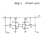
- FIG.1 shows an example of the static RAM formed in the conventional master slice type semiconductor integrated circuit having the sea of gates.
- a latch circuit is constituted by N-channel MOS transistors N1 and N2 and P-channel MOS transistors P1 and P2, and a transmission gate is constituted by N-channel MOS transistors N3 and N4.
- WL denotes a word line
- BL and XBL denote bit lines.
- the numbers of N-channel MOS transistors and P-channel MOS transistors used in the static RAM are not the same. As a result, the utilization efficiency of the basic cells is poor when forming the static RAM in the semiconductor integrated circuit having the sea of gates.
- the PLA has a two-level structure comprising ROMs in an AND plane and ROMs in an OR plane, and it is possible to generate various kinds of logic functions by use of a small number of transistors.
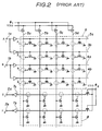
- FIG.2 shows an example of the conventional PLA.
- Input signals A i and B i are applied to terminals 1a and 1b.
- Signals A i , A i , B i and B i are supplied to input lines 3a, 3b, 4a and 4b, respectively.
- N-channel MOS transistors of an AND plane 6 are provided at intersections of the input lines 3a, 3b, 4a and 4b and product term lines 5a, 5b, 5c and 5d.
- N-channel MOS transistors of an OR plane 8 are provided at intersections of the product term lines 5a, 5b, 5c and 5d and output lines 7a and 7b.
- Output signals Z1 and Z2 are outputted from terminals 2a and 2b.
- the programming is carried out by connecting drains of the N-channel MOS transistors of the AND plane 6 to the respective product term lines 5a through 5d and connecting drains of the N-channels MOS transistors of the OR plane 8 to the respective output lines 7a and 7b at positions encircled by phantom lines.
- V DD denotes a power source voltage
- ⁇ 1 and ⁇ 2 denote clock signals of mutually different phases.
- the basic cells are basically formed in the CMOS structure for the formation of the logic unit cells.
- the basic cells are made of the same number of N-channel MOS transistors and P-channel MOS transistors. For this reason, when the PLA is formed by use of only the N-channel MOS transistors, the P-channel MOS transistors of the basic cells will not be used, and the utilization efficiency of the basic cells becomes poor.
- a plurality of transistors are arranged in an X-direction (column direction) within the basic cell, for example, and gates thereof are connected in common.
- the PLA gates of the plurality of transistors arranged in the column direction on the AND plane 6 are connected in common, and gates of the plurality of transistors arranged in a row direction on the OR plane 8 are connected in common.
- the PLA is not formed in the conventional master slice type semiconductor integrated circuit.
- Another and more specific object of the present invention is to provide a master slice type semiconductor integrated circuit which enables high utilization efficiency of basic cells when forming logic unit cells, RAMs, ROMs and the like in the semiconductor integrated circuit.
- Still another object of the present invention is to provide a master slice type semiconductor integrated circuit which enables high utilization efficiency of basic cells when forming a PLA in the semiconductor integrated circuit.
- the present invention relates to a master slice type semiconductor integrated circuit comprising a semiconductor chip, input/output cells arranged in a peripheral portion of the semiconductor chip, and basic cells arranged in a central portion of the semiconductor chip, each of said basic cells including a first portion containing complementary MOSFETs in the form of pairs of first and second N-channel MOSFETs and first and second P-channel MOSFETs, the P-channel MOSFETs of said pairs comprising first and second P-type regions spaced from each other in a first, column, direction by an N-type channel region oriented in a second direction perpendicular to said first direction insulatingly overlaid by a conductive gate electrode; the N-channel MOSFETs of said pairs comprising first and second N-type regions spaced from each other in said first column direction by an P-type channel region oriented in said second direction insulatingly overlaid by a conductive gate electrode; said first regions, second regions, channel regions, and gate electrodes of the N-channel MOSFETs of said pairs of said
- JP-A-58 139 446 the object of which is only to form a single port memory; however, the cell layout thereof is not particularly efficient.
- FR-A-2 393 427 which relates to an integrated circuit comprising basic cells the pattern of which can take four positions by rotation of 90° or 180°.
- the circuit of the present invention is further characterized in that said first and second N-type regions are spaced from each other in said first direction; and that the conductive gate electrode of said at least one MOSFET is offset in said first column direction from the conductive gates of any of the MOSFETs of said first portion containing complementary MOSFETs to allow one of said first or second N-type regions to be connected to one of said gate electrodes in said first portion directly by an interconnection aligned in said second direction.
- the utilization efficiency of the basic cell is extremely high when forming the logic unit cell, the RAM, the ROM and the like. There is virtually no unused or wasted portion of the basic cell, thereby greatly improving the integration density of the semiconductor integrated circuit.
- a circuit according to the invention can be arranged to be operable as a single port static random access memory, a dual port random access memory, a read only memory or a programmable logic array memory, as specified in claims 12 to 15, respectively.
- a single port static random access memory a dual port random access memory
- a read only memory a read only memory
- a programmable logic array memory as specified in claims 12 to 15, respectively.
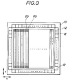
- FIG.3 generally shows an embodiment of the master slice type semiconductor integrated circuit according to the present invention.
- a semiconductor chip 10 comprises a plurality of input/output cells 12 provided in a peripheral portion of the chip 10 and a plurality of basic cells 20 provided in a central portion of the chip 10.
- FIGS.4 and 5 show an embodiment of the basic cells of the embodiment on an enlarged scale.
- FIGS.4 and 5 shows the so-called master on which no aluminum interconnection (wiring) has been formed.
- the master which is prepared is already formed with gate electrodes, and the aluminum interconnection is formed on an upper layer of the master depending on the needs of the user.
- V DD and V SS denote first and second power source voltages.
- V SS denotes the ground voltage.
- the basic cell 20 comprises a CMOS forming part 20a and an N-channel MOS (hereinafter simply referred to as an NMOS) forming part 20b.
- the CMOS forming part 20a is constituted by gate electrodes 21 and 22 indicated by a shading, a P-channel MOS (hereinafter simply referred to as a PMOS) part 23, and an NMOS part 24.
- the PMOS part 23 comprises P-channel portions 23a, 23b and 23c, and two PMOS transistors are formed using the P-channel portion 23c in common.
- the NMOS part 24 comprises N-channel portions 24a, 24b and 24c, and two NMOS transistors are formed using the N-channel portion 24c in common.
- the gate electrodes 21 and 22 respectively have wide portions 21a and 22a for connecting the interconnection on the upper layer in a slicing process.
- the NMOS forming part 20b is constituted by gate electrodes 25 and 26 indicated by a shading, and NMOS parts 27 and 28.
- the NMOS part 27 comprises N-channel portions 27a, 27b and 27c
- the NMOS part 28 comprises N-channel portions 28a, 28b and 28c.
- Two NMOS transistors are formed in the NMOS part 27 by using the N-channel portion 27c in common, and two NMOS transistors are formed in the NMOS part 28 by using the N-channel portion 28c in common.
- the gate electrodes 21, 22, 25 and 26 are made of polysilicon and are formed integrally.
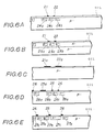
- FIGS.6A through 6E are cross sectional views of the basic cell along lines VIA-VIA, VIB-VIB, VIC-VIC, VID-VID and VIE-VIE in FIG.5, respectively.
- GIL denotes a gate insulator layer made of silicon dioxide (SiO2), for example.
- the width of the N-channel portion 27c in the Y-direction is two times that of the N-channel portion 28c, and two connecting portions can be provided both in the X and Y directions.
- first and second connecting portions are arranged in the Y-direction
- other interconnections such as bit lines on the remaining connecting portions arranged in the X-direction.
- the gate electrodes 25 and 26 are constituted by common electrodes which are integral parts of gates of the NMOS forming part 20b of the basic cell 20 which is adjacent on the left of the gate electrodes 25 and 26 in the X-direction. These gate electrodes 25 and 26 are provided with wide portions 25a and 26a, respectively.
- the two mutually adjacent NMOS forming parts 20b are point symmetrical about a point on a boundary between the two in a state where the two are shifted in the Y-direction.
- CMOS forming parts 20a of the basic cells 20 adjacent to each other in the X-direction are line symmetrical about a boundary line between the two.
- a plurality of the basic cells 20 are arranged in the X and Y directions in the entire central portion of the chip 10 as shown in FIG.3, excluding the regions of the input/output cells 12.
- a portion 29a is formed between the basic cells 20 adjacent to each other in the Y-direction, and a portion 29b is formed between the NMOS forming parts 20b (of the basic cells 20) adjacent to each other in the X-direction.
- the portions 29a and 29b are provided for making contacts to a substrate of the chip 10.
- FIG.4 only shows some of the contacts provided in the portions 29a and 29b.
- a contact CT1 is provided in the portion 29a for supplying the power source voltage V SS to the NMOS transistors in the CMOS forming part 20a.
- a contact CT2 is provided in the portion 29a for supplying the power source voltage V DD to the PMOS transistors in the CMOS forming part 20a.
- Contacts CT3 and CT4 are provided in the portion 29b for supplying the power source voltage V SS to the transistors of the NMOS forming part 20b.
- the interconnections for supplying the power source voltages V SS and V DD are illustrated as lines.
- rectangular marks indicate positions where a connection can be made with the aluminum interconnection.
- FIGS.7A and 7B show equivalent circuits of parts of the basic cell shown in FIG.5.
- FIG.7A shows an equivalent circuit of the CMOS forming part 20a.
- transistors Tr1 and Tr2 are NMOS transistors of the NMOS part 24, and transistors Tr3 and Tr4 are PMOS transistors of the PMOS part 23.
- FIG.7B shows an equivalent circuit of the pair of mutually adjacent NMOS forming parts 20b.
- transistors Tr5, Tr6, Tr11 and Tr12 are NMOS transistors of the NMOS part 28, and transistors Tr7, Tr8, Tr9 and Tr10 are NMOS transistors of the NMOS part 27.
- FIG.8A shows a row of basic cells 130, 131, 132 and 133 in the Y-direction.
- a and B respectively indicate the PMOS part 23 and the NMOS part 24 of the CMOS forming part 20a shown in FIG.3, and C indicates the NMOS forming part 20b.
- logic unit cells 134a and 134b are formed from the CMOS forming parts A and B as shown in FIG.8B, and the NMOS forming parts C are used as interconnection channels 135a and 135b.
- RAM cells 136a through 136d are formed from the basic cells 130 through 133, respectively, as shown in FIG.8C.
- ROM parts 137a through 137d are formed in the NMOS parts B and C as shown in FIG.8D.
- the ROM parts 137a through 137d have a plurality of cells in each of the NMOS parts B and C, and the CMOS part A is not used.
- the two mutually adjacent NMOS forming parts 20b are point symmetrical about the point on the boundary between the two in the state where the two are shifted in the Y-direction, and further, the CMOS forming parts 20a of the basic cells 20 adjacent to each other in the X-direction are line symmetrical about the boundary line between the two.
- CAD computer aided design
- the same interconnection can be used for a device having an arrangement shown in FIG.9B, for example, by rotating the interconnection 180°.
- CCT1 and CCT2 denote circuit parts constituted by the basic cells.
- the number of terminals becomes extremely large when the number of bits is large, and it would be both time consuming and troublesome to design interconnections for every user's needs. But according to the present embodiment, it is possible to use the same interconnection for arrangements having a certain relationship such as that of FIGS.9A and 9B.
- the peripheral circuits such as the address decoder.
- the interconnection used for the address decoder provided with respect to one of the two ports can be rotated and used for the address decoder provided with respect to the other of the two ports.
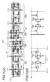
- FIGS.10A and 10B are a wiring diagram and a circuit diagram of 1-port static RAM cells using the basic cells of the present embodiment.
- FIG.10A and the wiring diagrams shown in FIGS.12A and 14A which will be described later the illustration of the gate electrode is omitted for convenience' sake, and the connecting positions of the interconnection correspond to the rectangular mark in FIG.5. Furthermore, a hatching indicates a first layer aluminum interconnection and a shading indicates a second layer aluminum interconnection.
- the P-channel portion 23c and the N-channel portion 24c of the respective PMOS part 23 and the NMOS part 24 in FIG.10A are respectively connected to the power source voltages V DD and V SS at connecting portions C11 and C12.
- a latch circuit LAT shown in FIG.10B formed by the CMOS forming part 20a is driven by the power source voltages V DD and V SS .
- the latch circuit LAT comprises PMOS transistors P1 and P2 and NMOS transistors N1 and N2.
- the NMOS parts 28 and 27 of the NMOS forming part 20b respectively constitute transmission gates N3 and N4, and gates of these transmission gates N3 and N4 are connected to a word line WL1 at the connecting portion C1.
- the N-channel portions 27a and 27b are connected to a bit line XBL3 at a connecting portion C2, and the N-channel portions 28a and 28b are connected to a bit line BL3 at a connecting portion C3.
- the N-channel portions 27c and 28c are connected to the latch circuit LAT at respective connecting portions C4 and C5.
- the 1-port static RAM cell amounting to one bit is constituted by using all of the basic cell 20.
- FIG.11A shows a portion of the pattern shown in FIG.10A with the connections indicated by lines so as to facilitate the understanding of FIG.10A.
- FIG.11B is a circuit diagram showing the equivalent circuit of FIG.11A.
- FIGS.11A and 11B those parts which are the same as those corresponding parts in FIGS.10A and 10B are designated by the same reference numerals, and a description thereof will be omitted.
- the transistors formed at a location Q1 are shifted upwardly in the figures compared to the transistors formed at a location Q2, thereby preventing the increase in the space occupied by the transistors in the horizontal direction in the figures.
- the portion 29a essentially formed by the vertical positional difference between the locations Q1 and Q2 is effectively used for providing the contact as described before in conjunction with FIG.4.
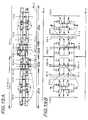
- FIGS.12A and 12B are a wiring diagram and a circuit diagram of 2-port static RAM cells using the basic cells of the present embodiment.
- FIGS.12A and 12B differ from FIGS.10A and 10B in the following respects. That is, two word lines WL1 and WL2 are provided, and four bit lines BL3, XBL3, BL4 and XBL4 are provided for one bit.
- the gates of the transmission gates N3 and N4 formed in the respective NMOS parts 28 and 27 are connected in common to the word line WL1 at the connecting portion C1.
- the N-channel portions 28b and 27b of the NMOS parts 28 and 27 are connected to the bit lines BL3 and XBL3 at respective connecting portions C6 and C7.
- gates of transmission gates N5 and N6 are connected in common to the word line WL2 at a connecting portion C8, and the N-channel portions 28a and 27a of the NMOS parts 28 and 27 are connected to the bit lines BL4 and XBL4 at respective connecting portions C9 and C10.
- the 2-port static RAM cell amounting to one bit is constituted by using all of the basic cell 20.
- FIG.13A shows a portion of the pattern shown in FIG.12A with the connections indicated by lines so as to facilitate the understanding of FIG.12A.
- FIG.13B is a circuit diagram showing the equivalent circuit of FIG.13A.
- FIGS.13A and 13B those parts which are the same as those corresponding parts in FIGS.12A and 12B are designated by the same reference numerals, and a description thereof will be omitted.
- FIGS.14A and 14B are a wiring diagram and a circuit diagram of ROM cells using the basic cells of the present embodiment.
- Sources of NMOS transistors N10 and N11 formed by the NMOS part 24 and sources of NMOS transistors N12 and N13 formed by the NMOS parts 27 and 28 are connected in common to the power source voltage V SS at connecting portions C20 through C24.
- P-channel portions 23a, 23b and 23c of the PMOS part 23 are connected to the power source voltage V DD so that the PMOS transistor will not operate.
- the gates of the NMOS transistors N10 and N12 are connected to the word line WL1 at connecting portions C25 through C27.
- the NMOS transistors N11 and N13 are connected to the word line WL2 at connecting portions C28 through C30.
- the ROM cell is programmed depending on whether or not drains of the NMOS transistors N10 and N11 (N-channel portions 24a and 24b) are connected to the bit line BL4 and whether or not drains of the NMOS transistors N12 and N13 (N-channel portions 27a, 27b, 28a and 28b) are connected to the bit line BL3. In other words, the ROM cell is programmable.
- FIG.15 shows a portion of the pattern shown in FIG.14A with the connections indicated by lines so as to facilitate the understanding of FIG.14A.
- those parts which are the same as those corresponding parts in FIGS.14A and 14B are designated by the same reference numerals, and a description thereof will be omitted.
- circular marks other than the black circular marks denote program contacts where a contact can be made depending on the programming which is carried out.
- the unused NMOS forming part 20b which is not used for the logic unit cells can be effectively utilized as the interconnection channels.
- 100% of the basic cell 20 can be used, and there is no unused or wasted portions of the basic cell 20.
- forming the ROM virtually all of the basic cells can be used except for the PMOS part 23. Hence, the utilization efficiency of the basic cells 20 is extremely high according to the present embodiment.
- the logic unit cell, the RAM cell, the ROM cell and the like can be formed by use of the basic cell 20, with a similar utilization efficiency to that of the embodiment described before.
- the utilization efficiency of the basic cell is extremely high when forming the logic unit cell, the RAM, the ROM and the like. There is virtually no unused or wasted portion of the basic cell, thereby greatly improving the integration density of the semiconductor integrated circuit.
- FIGS.16 and 17 are a wiring diagram and a circuit diagram respectively showing a first embodiment of the PLA.
- FIGS.16 and 17 those parts which are the same as those corresponding parts in FIGS.3 through 5 are designated by the same reference numerals, and a description thereof will be omitted.
- the illustration of the gate electrode is omitted for convenience' sake, and the connecting position of the interconnection corresponds to the rectangular mark in FIG.5.
- a hatching indicates a first layer aluminum interconnection (wiring)
- a shading indicates a second layer aluminum interconnection (wiring).
- a first column 40 of the basic cells 20 and a second column 41 of the basic cells 20 constitute an AND plane 44
- a third column 42 of the basic cells 20 and a fourth column 43 of the basic cells 20 constitute an OR plane 45.
- the p-channel portions 23a, 23b and 23c of the PMOS part 23 are connected to the power source voltage V DD so that the PMOS transistor does not operate.
- N-channel portions 24c, 27c and 28c of the respective NMOS parts 24, 27 and 28 are connected to the power source voltage V SS .
- An input line 46 which extends in the X-direction and receives a signal A j is connected to the gate electrodes 21 and 25 at the connecting portions C1 and C2.
- An input line 47 which extends in the X-direction and receives a signal A j is connected to the gate electrodes 22 and 26 at the connecting portions C3 and C4. Accordingly, the two NMOS transistors N1 and N2 shown in FIG.18 are formed at the N-channel portions 24a and 24c and N-channel portions 24b and 24c of the NMOS part 24.
- the two NMOS transistors N3 and N4 are formed at the N-channel portions 27b, 28b, 27c and 28c of the NMOS parts 27 and 28 and the N-channel portions 27a, 28a, 27c and 28c of the N-channel parts 27 and 28.
- Product term lines 48 and 49 are provided on the respective NMOS parts 24 and 27 and extend in the Y-direction.
- the programming of the PLA is carried out by connecting the drains of the NMOS transistors N1 through N4 to the product term lines 48 and 49 at the connecting portions C5 through C8.
- portions where the programming is carried out are encircled by phantom lines.
- the arrangement is similar for the second column 41 in which input lines 50 and 51 extend in the Y-direction.
- the P-channel portions 23a, 23b and 23c of the PMOS part 23 are connected to the power source voltage V DD so that the PMOS transistor does not operate.
- N-channel portions 24c, 27c and 28c of the respective NMOS parts 24, 27 and 28 are connected to the power source voltage V SS .
- An output line 52 which extends in the X-direction and outputs a signal Z 1 is connected to the N-channel portion 24c, the N-channel portions 28b and 27b and the N-channel portions 28a and 27a at the connecting portion C10, the connecting portions C11 and C12 and the connecting portion C13. Accordingly, the NMOS transistor N10 shown in FIG.17 is formed by the NMOS part 24, and the NMOS transistor N11 is formed by the NMOS parts 27 and 28.
- Product term lines 53 and 54 extend in the Y-direction on the wide portions 21a and 22a of the CMOS forming part 20a. These product term lines 53 and 54 are respectively connected to the product term lines 48 and 49.
- the programming is carried out by connecting the gates of the transistors N10 and N11 to the product term lines 53 and 54 at the connecting portions C15 and C16 and the connecting portions C17 and C18.
- the arrangement is similar for the fourth column 43 in which an output line 55 extends in the Y-direction.
- the basic cell 20 has the CMOS forming part 20a and the NMOS forming part 20b, and the utilization efficiency of the basic cells 20 is greatly improved because there are more NMOS transistors constituted by the basic cells 20 than PMOS transistors.
- FIG.18 shows a portion of the pattern shown in FIG.16 with the connections indicated by lines so as to facilitate the understanding of FIG.16.
- those parts which are the same as those corresponding parts in FIG.16 are designated by the same reference numerals, and a description thereof will be omitted.
- FIG.19 is a circuit diagram of a second embodiment of the PLA.
- terminals 60 and 60′ receive the input signals A j and B j , and the signals A j , A j , B j and B j are respectively supplied to input lines 61 through 64 extending in the X-direction.
- the input lines 61 through 64 extend in the Y-direction and cross perpendicularly to product term lines 65a through 68a.
- NMOS transistors of an AND plane 70 are provided at intersections of the input lines 61 through 64 and the product term lines 65a through 68a.
- Product term lines 65b through 68b which extend in the X-direction are respectively connected to the product term lines 65a through 68a.
- Output lines 72 and 73 which are provided on the right of the product term lines 65a through 68a in the X-direction extend in the Y-direction and cross perpendicularly to the product term lines 65b through 68b.
- NMOS transistors of an OR plane 71 are provided at the intersections of the output lines 72 and 73 and the product term lines 65b through 68b.
- the NMOS transistors of the AND plane 70 have gates thereof grounded and respectively connected to the input lines 61 through 64.
- the programming is carried out by connecting drains of the NMOS transistors to the respective product term lines 65a through 68a at portions encircled by phantom lines.
- the NMOS transistors of the OR plane 71 have sources thereof grounded and respectively connected to the product term lines 65b through 68b.
- the programming is carried out by connecting drains of the NMOS transistors of the OR plane 71 to the respective output lines 72 and 73.
- Clock signals ⁇ 1 and ⁇ 2 having mutually different phases are applied to terminals 74 and 75, respectively.
- the output signals Z1 and Z2 are outputted from respective terminals 76 and 77.
- the product term lines 65a through 68a for the AND plane 70 and the product term lines 65b through 68b are provided for the OR plane 71 which cross perpendicularly to the product term lines 65a through 68a.
- the AND plane 70 and the OR plane 71 in the X-direction, and the NMOS transistors formed from the basic cells 20 shown in FIGS.3 through 5 can be used efficiently in both the AND plane 70 and the OR plane 71.
- FIG.20 is a circuit diagram of a third embodiment of the PLA.
- those parts which are the same as those corresponding parts in FIG.19 are designated by the same reference numerals, and a description thereof will be omitted.
- the product term lines 65b through 68b which extend in the X-direction are arranged below the AND plane 70 and are connected to the product term lines 65a through 68a. Accordingly, it is possible to arrange the OR plane 71 in the Y-direction to the AND plane 70, and the basic cells 20 can be utilized efficiently both in the AND plane 70 and the OR plane 71 as in the case of the second embodiment of the PLA.
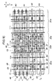
- FIG. 21A shows a portion of a fourth embodiment of the PLA with the connections indicated by lines to facilitate the understanding thereof.
- FIG.21B is a circuit diagram showing the equivalent circuit of FIG.21A.
- P1 denotes a product term line
- I1, XI1, I2 and XI2 denote input lines
- O1 through O8 denote output lines.
- the large and small transistors of the basic cells are used for both the AND plane and the OR plane. But in the present embodiment, the large transistors are used for the AND plane, and the small transistors are used only for the OR plane.
- the number of output lines is greater than the number of input lines.
- the embodiments of the PLA it is possible to constitute the PLA by the master slice type semiconductor integrated circuit by efficiently utilizing the basic cells. As a result, the field of application of the master slice type semiconductor integrated circuit is considerably expanded.
Landscapes
- Design And Manufacture Of Integrated Circuits (AREA)
- Metal-Oxide And Bipolar Metal-Oxide Semiconductor Integrated Circuits (AREA)
Claims (15)
- Eine integrierte Halbleiterschaltung des Master-Slice-Typs mit:- einem Halbleiterchip (10);- Eingabe-/Ausgabezellen (12), die in einem peripheren Abschnitt des genannten Halbleiterchips angeordnet sind; und- Basiszellen (20), die in einem zentralen Abschnitt des genannten Halbleiterchips angeordnet sind,bei der jede der genannten Basiszellen einen ersten Abschnitt (20a) umfaßt, der komplementäre MOSFETs in der Form von Paaren von ersten und zweiten N-Kanal-MOSFETs und ersten und zweiten P-Kanal-MOSFETs enthält,
welche P-Kanal-MOSFETs der genannten Paare erste und zweite P-Typ-Zonen umfassen, die in einer ersten Richtung, einer Spaltenrichtung (Y) durch eine N-Typ-Kanalzone räumlich voneinander getrennt angeordnet sind, die in einer zweiten Richtung (X) rechtwinklig zu der genannten ersten Richtung ausgerichtet ist, von einer leitfähigen Gateelektrode (21, 22) isolierend überlagert;
welche N-Kanal-MOSFETs der genannten Paare erste und zweite N-Typ-Zonen umfassen, die in der genannten ersten Spaltenrichtung, durch eine P-Typ-Kanalzone räumlich voneinander getrennt angeordnet sind, die in der genannten zweiten Richtung ausgerichtet ist, von einer leitfähigen Gateelektrode (21, 22) isolierend überlagert;
welche ersten Zonen, zweiten Zonen, Kanalzonen und Gateelektroden der N-Kanal-MOSFETs der genannten Paare angrenzend an die genannten ersten Zonen, zweiten Zonen, Kanalzonen bzw. Gateelektroden der P-Kanal-MOSFETs der genannten Paare in der genannten zweiten Richtung (X) angeordnet sind;
bei der jede der genannten Basiszellen ferner einen zweiten Abschnitt (20b) umfaßt, der dritte und vierte MOSFETs des NMOS-Typs enthält;
welcher zweite Abschnitt von jeder der genannten Basiszellen angrenzend an den genannten ersten Abschnitt einer jeweiligen der genannten Basiszellen in der genannten zweiten Richtung (X) angeordnet ist;
welcher zweite Abschnitt von jeder der genannten Basiszellen wenigstens einen MOSFET enthält, der erste und zweite N-Typ-Zonen (28b, 28c) umfaßt, die durch eine P-Typ-Kanalzone räumlich voneinander getrennt angeordnet sind, von einer leitfähigen Gateelektrode isolierend überlagert; dadurch gekennzeichnet, daß die genannten ersten und zweiten N-Typ-Zonen des genannten zweiten Abschnittes in der genannten ersten Richtung (Y) räumlich voneinander getrennt angeordnet sind; und daß die leitfähige Gateelektrode des genannten wenigstens einen MOSFET in der genannten ersten Spaltenrichtung, (Y) von den leitfähigen Gates jeglicher MOSFETs des genannten ersten Abschnittes (20a), der komplementäre MOSFETs enthält, versetzt ist, um eine der genannten ersten (28b) oder zweiten (28c) N-Typ-Zonen des genannten zweiten Abschnittes mit einer der genannten Gateelektroden (22a) in dem genannten ersten Abschnitt direkt durch eine Zwischenverbindung verbinden zu können, die in der genannten zweiten Richtung ausgerichtet ist. - Eine integrierte Halbleiterschaltung des Master-Slice-Typs nach Anspruch 1, bei der die leitfähige Gateelektrode des genannten P-Kanal-MOSFET und die leitfähige Gateelektrode des genannten N-Kanal-MOSFET in jedem der genannten Paare durch eine gemeinsame Elektrode integral gebildet sind.
- Eine integrierte Halbleiterschaltung des Master-Slice-Typs nach Anspruch 1, bei der die genannten Basiszellen eine Vielzahl von Basiszellenspalten bilden, die in einer Richtung (X) angeordnet sind, die zu der genannten ersten Richtung, der Spaltenrichtung, (Y) rechtwinklig ist, so daß die genannten ersten Abschnitte (20a) der genannten aneinandergrenzenden Basiszellenspalten aneinandergrenzen und die genannten zweiten Abschnitte (20b) der genannten aneinandergrenzenden Basiszellenspalten aneinandergrenzen.
- Eine integrierte Halbleiterschaltung des Master-Slice-Typs nach Anspruch 3, bei der zwischen zweien der genannten Basiszellenspalten mit aneinandergrenzenden ersten Abschnitten (20a) die leitfähige Gateelektrode (25, 26) des genannten zweiten Abschnittes (20b) in einer der genannten zwei Basiszellenspalten und die leitfähige Gateelektrode (25, 26) des genannten zweiten Abschnittes (20b) in der anderen der genannten zwei Basiszellenspalten längs der genannten ersten Spaltenrichtung, (Y) versetzt sind.
- Eine integrierte Halbleiterschaltung des Master-Slice-Typs nach Anspruch 3, bei der zwischen zweien der genannten Basiszellenspalten mit aneinandergrenzenden zweiten Abschnitten (20b) die leitfähige Gateelektrode (25, 26) des genannten zweiten Abschnittes (20b) in einer der genannten zwei Basiszellenspalten und die leitfähige Gateelektrode (25, 26) des genannten zweiten Abschnittes in der anderen der genannten zwei Basiszellenspalten längs der genannten ersten Spaltenrichtung, (Y) versetzt sind.
- Eine integrierte Halbleiterschaltung des Master-Slice-Typs nach Anspruch 1, bei der in dem genannten ersten Abschnitt die genannte zweite Zone des genannten ersten P-Kanal-MOSFET und die genannte erste Zone des genannten zweiten P-Kanal-MOSFET durch eine gemeinsame P-Typ-Zone (24c) gebildet sind, und die genannte zweite Zone des genannten zweiten N-Kanal-MOSFET und die genannte erste Zone des genannten ersten N-Kanal-MOSFET durch eine gemeinsame N-Typ-Zone (23c) gebildet sind.
- Eine integrierte Halbleiterschaltung des Master-Slice-Typs nach Anspruch 6, bei der der genannte zweite Abschnitt (20b) ferner fünfte und sechste N-Kanal-MOSFETs enthält, welche dritten und vierten N-Kanal-MOSFETs in der genannten ersten Richtung, der Spaltenrichtung, angeordnet sind und erste (28a), zweite (28b) und dritte (28c) N-Typ-Zonen enthalten, welche fünften und sechsten N-Kanal-MOSFETs in der genannten ersten Spaltenrichtung, getrennt von den genannten dritten und vierten N-Kanal-MOSFETs in der genannten zweiten Richtung (X) angeordnet sind und vierte (27a), fünfte (27b) und sechste (27c) N-Typ-Zonen enthalten, und welche vierten und sechsten N-Kanal-MOSFETs leitfähige Gateelektroden haben, die in der genannten ersten Spaltenrichtung, versetzt sind.
- Eine integrierte Halbleiterschaltung des Master-Slice-Typs nach Anspruch 7, bei der die genannten leitfähigen Gateelektroden der genannten dritten und fünften N-Kanal-MOSFETs durch eine lineare integrale Elektrode gebildet sind und die genannten vierten und sechsten N-Kanal-MOSFETs leitfähige Gateelektroden haben, die durch eine integrale Elektrode gebildet sind.
- Eine integrierte Halbleiterschaltung des Master-Slice-Typs nach Anspruch 8, bei der die genannten Basiszellen eine Vielzahl von Basiszellenspalten bilden, die in einer Richtung angeordnet sind, die zu der genannten ersten Spaltenrichtung, rechtwinklig ist, die genannten leitfähigen Gateelektroden der genannten vierten und sechsten N-Kanal-MOSFETs in dem genannten zweiten Abschnitt einer der genannten Basiszellen und die genannten leitfähigen Gateelektroden der genannten vierten und sechsten N-Kanal-MOSFETs in dem genannten zweiten Abschnitt einer angrenzenden Basiszelle jeweils durch eine integrale gemeinsame Elektrode gebildet sind; und die genannten leitfähigen Gateelektroden der genannten dritten und fünften N-Kanal-MOSFETs der genannten einen der genannten Basiszellen und die genannten leitfähigen Gateelektroden der genannten dritten und fünften N-Kanal-MOSFETs der genannten angrenzenden Basiszelle jeweils durch eine integrale gemeinsame Elektrode gebildet sind.
- Eine integrierte Halbleiterschaltung des Master-Slice-Typs nach Anspruch 7, bei der die Breite der genannten leitfähigen Gateelektrode in der genannten ersten Richtung auf beiden Seiten der genannten Kanalzone längs der genannten zweiten Richtung größer als jene an einem Teil ist, der die genannte Kanalzone für jeden der genannten P-Kanal-MOSFETs und der genannten N-Kanal-MOSFETs überlagert, um Gateelektrodenkontaktzonen zu definieren.
- Eine integrierte Halbleiterschaltung des Master-Slice-Typs nach Anspruch 7, bei der die Breite der genannten leitfähigen Gateelektrode der genannten P-Kanal- und N-Kanal-MOSFETs innerhalb des genannten ersten Abschnittes längs der genannten zweiten Richtung größer als die Breite der genannten leitfähigen Gateelektrode der genannten MOSFETs innerhalb des genannten zweiten Abschnittes längs der genannten zweiten Richtung ist.
- Eine integrierte Halbleiterschaltung des Master-Slice-Typs nach Anspruch 1, die als statischer Einzelportspeicher mit wahlfreiem Zugriff betriebsfähig ist und umfaßt:
eine Wortleitung (WL1);
eine Vielzahl von Bitleitungen (BL3, XBL3, ...);
eine erste Energiequellenleitung zum Empfangen einer ersten Energiequellenspannung (VDD); und
eine zweite Energiequellenleitung zum Empfangen einer zweiten Energiequellenspannung (VSS);
bei der jede der genannten Basiszellen eine Speicherzelle bildet, die eine Verriegelungsschaltung enthält, die durch zwei Paare (P1, N1, P2, N2) von N-Kanal-MOSFETs und P-Kanal-MOSFETs innerhalb des genannten ersten Abschnittes gebildet ist,
jeder der genannten N-Kanal-MOSFETs innerhalb des genannten zweiten Abschnittes ein Übertragungsgate bildet, das mit einer entsprechenden der Bitleitungen (BL3, ...) verbunden ist,
jedes der genannten Übertragungsgates mit der Verriegelungsschaltung einer Speicherzelle gekoppelt ist und mit einer gemeinsamen Wortleitung (WL1) verbunden ist,
die N-Typ-Kanalzone (23c) des P-Kanal-MOSFET mit der genannten ersten Energiequellenleitung (VDD) verbunden ist,
die P-Typ-Kanalzone des N-Kanal-MOSFET mit der genannten zweiten Energiequellenleitung (VSS) verbunden ist. - Eine integrierte Halbleiterschaltung des Master-Slice-Typs nach Anspruch 1, die als Dualportspeicher mit wahlfreiem Zugriff betriebsfähig ist und umfaßt:
eine Vielzahl von Wortleitungen (WL1,WL2, ...);
eine Vielzahl von Bitleitungen (BL1, XBL1, BL3, ...);
eine erste Energiequellenleitung zum Empfangen einer ersten Energiequellenspannung (VDD); und
eine zweite Energiequellenleitung zum Empfangen einer zweiten Energiequellenspannung (VSS);
bei der jede der genannten Basiszellen eine Speicherzelle bildet, die eine Verriegelungsschaltung enthält, die durch die genannten zwei Paare (P1, N1, P2, N2) von N-Kanal-MOSFETs und P-Kanal-MOSFETs innerhalb des genannten ersten Abschnittes gebildet ist,
jeder der genannten N-Kanal-MOSFETs (N3, N4, N5, N6) innerhalb des genannten zweiten Abschnittes ein Übertragungsgate bildet, das mit einer entsprechenden der Bitleitungen (BL1, ...) und mit einer entsprechenden der Wortleitungen (WL1, ...) gekoppelt ist,
die N-Typ-Kanalzone des P-Kanal-MOSFET mit der genannten ersten Energiequellenleitung verbunden ist,
die P-Typ-Kanalzone des N-Kanal-MOSFET mit der genannten zweiten Energiequellenleitung verbunden ist. - Eine integrierte Halbleiterschaltung des Master-Slice-Typs nach Anspruch 1, die als Nur-Lese-Speicher betriebsfähig ist und umfaßt:
eine Vielzahl von Wortleitungen (WL1, WL2, ...);
eine Vielzahl von Bitleitungen (BL3, BL4, ...);
eine erste Energiequellenleitung zum Empfangen einer ersten Energiequellenspannung; und
eine zweite Energiequellenleitung zum Empfangen einer zweiten Energiequellenspannung;
bei der jede der genannten Basiszellen Speicherzellen durch die genannten N-Kanal-MOSFETs (N10, N11, ...) innerhalb des genannten zweiten Abschnittes bildet,
jede der genannten Speicherzellen mit einer der Wortleitungen (WL1, ...) und mit einer der Bitleitungen (BL3, ...) verbunden ist,
die genannte erste Energiequellenleitung gemeinsam mit den Sourcezonen der N-Kanal-MOSFETs innerhalb der genannten ersten und zweiten Abschnitte verbunden ist,
die genannte zweite Energiequellenleitung gemeinsam mit den ersten und zweiten P-Typ-Zonen der P-Kanal-MOSFETs innerhalb des genannten ersten Abschnittes verbunden ist. - Eine integrierte Halbleiterschaltung des Master-Slice-Typs nach Anspruch 1, die als programmierbares Logikarray betriebsfähig ist und umfaßt:
Eingangsleitungen (46, 47);
erste Produkttermleitungen (48, 49);
zweite Produkttermleitungen (53, 54), die mit den genannten ersten Produkttermleitungen verbunden sind;
eine UND-Ebene (44) mit ersten und zweiten Spalten der genannten Basiszellen;
eine ODER-Ebene (45) mit dritten und vierten Spalten der genannten Basiszellen;
bei der jede der genannten Basiszellen in dem zweiten Abschnitt vier N-Kanal-MOSFETs und eine Ausgangsleitung (52) enthält.
Applications Claiming Priority (4)
| Application Number | Priority Date | Filing Date | Title |
|---|---|---|---|
| JP62142499A JPS63306640A (ja) | 1987-06-08 | 1987-06-08 | プログラマブル・ロジック・アレイ |
| JP62142493A JPH0795589B2 (ja) | 1987-06-08 | 1987-06-08 | マスタスライス型半導体集積回路 |
| JP142493/87 | 1987-06-08 | ||
| JP142499/87 | 1987-06-08 |
Publications (3)
| Publication Number | Publication Date |
|---|---|
| EP0295183A2 EP0295183A2 (de) | 1988-12-14 |
| EP0295183A3 EP0295183A3 (en) | 1990-07-11 |
| EP0295183B1 true EP0295183B1 (de) | 1994-10-12 |
Family
ID=26474477
Family Applications (1)
| Application Number | Title | Priority Date | Filing Date |
|---|---|---|---|
| EP88401399A Expired - Lifetime EP0295183B1 (de) | 1987-06-08 | 1988-06-08 | Integrierte-Masterslice-Halbleiterschaltung mit einem Meer von Gates |
Country Status (3)
| Country | Link |
|---|---|
| EP (1) | EP0295183B1 (de) |
| KR (1) | KR910005605B1 (de) |
| DE (1) | DE3851788T2 (de) |
Cited By (1)
| Publication number | Priority date | Publication date | Assignee | Title |
|---|---|---|---|---|
| US9479176B1 (en) | 2013-12-09 | 2016-10-25 | Rambus Inc. | Methods and circuits for protecting integrated circuits from reverse engineering |
Families Citing this family (1)
| Publication number | Priority date | Publication date | Assignee | Title |
|---|---|---|---|---|
| JP4279955B2 (ja) * | 1998-12-08 | 2009-06-17 | 富士通マイクロエレクトロニクス株式会社 | 半導体集積回路装置及びその製造方法 |
Family Cites Families (2)
| Publication number | Priority date | Publication date | Assignee | Title |
|---|---|---|---|---|
| DE2823555A1 (de) * | 1977-05-31 | 1978-12-07 | Fujitsu Ltd | Zellenfoermige integrierte schaltung |
| JPS62122419A (ja) * | 1985-11-22 | 1987-06-03 | Nec Corp | プログラマブルロジツクアレイ |
-
1988
- 1988-06-07 KR KR8806804A patent/KR910005605B1/ko not_active Expired
- 1988-06-08 DE DE3851788T patent/DE3851788T2/de not_active Expired - Fee Related
- 1988-06-08 EP EP88401399A patent/EP0295183B1/de not_active Expired - Lifetime
Cited By (1)
| Publication number | Priority date | Publication date | Assignee | Title |
|---|---|---|---|---|
| US9479176B1 (en) | 2013-12-09 | 2016-10-25 | Rambus Inc. | Methods and circuits for protecting integrated circuits from reverse engineering |
Also Published As
| Publication number | Publication date |
|---|---|
| KR890001292A (ko) | 1989-03-20 |
| DE3851788T2 (de) | 1995-02-09 |
| EP0295183A3 (en) | 1990-07-11 |
| EP0295183A2 (de) | 1988-12-14 |
| DE3851788D1 (de) | 1994-11-17 |
| KR910005605B1 (en) | 1991-07-31 |
Similar Documents
| Publication | Publication Date | Title |
|---|---|---|
| US4884115A (en) | Basic cell for a gate array arrangement in CMOS Technology | |
| US4791607A (en) | Gate array integrated circuit device and method thereof for providing various bit/word constructions | |
| US4780846A (en) | Master slice type semiconductor circuit device | |
| US5930163A (en) | Semiconductor memory device having two P-well layout structure | |
| US6469328B2 (en) | Semiconductor memory device | |
| US6822300B2 (en) | Semiconductor memory device | |
| KR900000202B1 (ko) | 반도체 집적회로 및 그 회로 패턴 설계방법 | |
| US6590802B2 (en) | Semiconductor storage apparatus | |
| JP2004072117A (ja) | Soi基板上のメモリ | |
| US4780851A (en) | Semiconductor memory device having improved redundant structure | |
| US5053993A (en) | Master slice type semiconductor integrated circuit having sea of gates | |
| EP0523967B1 (de) | Anordnung von Transistoren zur Fertigung einer Basiszelle für eine integrierte Masterslice-Halbleiteranordnung und integrierte Masterslice-Halbleiteranordnung | |
| JPH0358184B2 (de) | ||
| US5621697A (en) | High density integrated circuit with bank select structure | |
| EP0359204A2 (de) | Halbleiterspeicheranordnung, welche ein Herabsetzen der Anzahl mangelhafter Bits erlaubt | |
| EP0295183B1 (de) | Integrierte-Masterslice-Halbleiterschaltung mit einem Meer von Gates | |
| EP0092176A2 (de) | Basiszelle für integrierte Verknüpfungsschaltungsfelder | |
| US4924440A (en) | MOS gate array devices | |
| JPH0568862B2 (de) | ||
| JP2868016B2 (ja) | ゲートアレイの基本セル | |
| JPH0329187B2 (de) | ||
| JP3579068B2 (ja) | 論理回路 | |
| JPH06140592A (ja) | 半導体装置 | |
| KR0178815B1 (ko) | 레벨간 절연층에서 선택적으로 신장하는 디지트 라인을 갖는 반도체 ram 장치 | |
| JP2720104B2 (ja) | 半導体集積回路装置のメモリセル回路 |
Legal Events
| Date | Code | Title | Description |
|---|---|---|---|
| PUAI | Public reference made under article 153(3) epc to a published international application that has entered the european phase |
Free format text: ORIGINAL CODE: 0009012 |
|
| AK | Designated contracting states |
Kind code of ref document: A2 Designated state(s): DE FR GB |
|
| PUAL | Search report despatched |
Free format text: ORIGINAL CODE: 0009013 |
|
| AK | Designated contracting states |
Kind code of ref document: A3 Designated state(s): DE FR GB |
|
| 17P | Request for examination filed |
Effective date: 19901129 |
|
| 17Q | First examination report despatched |
Effective date: 19920124 |
|
| GRAA | (expected) grant |
Free format text: ORIGINAL CODE: 0009210 |
|
| AK | Designated contracting states |
Kind code of ref document: B1 Designated state(s): DE FR GB |
|
| REF | Corresponds to: |
Ref document number: 3851788 Country of ref document: DE Date of ref document: 19941117 |
|
| ET | Fr: translation filed | ||
| PLBE | No opposition filed within time limit |
Free format text: ORIGINAL CODE: 0009261 |
|
| STAA | Information on the status of an ep patent application or granted ep patent |
Free format text: STATUS: NO OPPOSITION FILED WITHIN TIME LIMIT |
|
| 26N | No opposition filed | ||
| PGFP | Annual fee paid to national office [announced via postgrant information from national office to epo] |
Ref country code: GB Payment date: 19980601 Year of fee payment: 11 |
|
| PGFP | Annual fee paid to national office [announced via postgrant information from national office to epo] |
Ref country code: FR Payment date: 19980609 Year of fee payment: 11 |
|
| PGFP | Annual fee paid to national office [announced via postgrant information from national office to epo] |
Ref country code: DE Payment date: 19980612 Year of fee payment: 11 |
|
| PG25 | Lapsed in a contracting state [announced via postgrant information from national office to epo] |
Ref country code: GB Free format text: LAPSE BECAUSE OF NON-PAYMENT OF DUE FEES Effective date: 19990608 |
|
| PG25 | Lapsed in a contracting state [announced via postgrant information from national office to epo] |
Ref country code: FR Free format text: THE PATENT HAS BEEN ANNULLED BY A DECISION OF A NATIONAL AUTHORITY Effective date: 19990630 |
|
| GBPC | Gb: european patent ceased through non-payment of renewal fee |
Effective date: 19990608 |
|
| PG25 | Lapsed in a contracting state [announced via postgrant information from national office to epo] |
Ref country code: DE Free format text: LAPSE BECAUSE OF NON-PAYMENT OF DUE FEES Effective date: 20000503 |
|
| REG | Reference to a national code |
Ref country code: FR Ref legal event code: ST |