EP0297802A2 - Isoliertes lichtzündbares Thyristor-Modul - Google Patents
Isoliertes lichtzündbares Thyristor-Modul Download PDFInfo
- Publication number
- EP0297802A2 EP0297802A2 EP88305818A EP88305818A EP0297802A2 EP 0297802 A2 EP0297802 A2 EP 0297802A2 EP 88305818 A EP88305818 A EP 88305818A EP 88305818 A EP88305818 A EP 88305818A EP 0297802 A2 EP0297802 A2 EP 0297802A2
- Authority
- EP
- European Patent Office
- Prior art keywords
- anode
- thyristor
- housing
- semiconductor body
- cathode
- Prior art date
- Legal status (The legal status is an assumption and is not a legal conclusion. Google has not performed a legal analysis and makes no representation as to the accuracy of the status listed.)
- Withdrawn
Links
Images


Classifications
-
- H—ELECTRICITY
- H10—SEMICONDUCTOR DEVICES; ELECTRIC SOLID-STATE DEVICES NOT OTHERWISE PROVIDED FOR
- H10F—INORGANIC SEMICONDUCTOR DEVICES SENSITIVE TO INFRARED RADIATION, LIGHT, ELECTROMAGNETIC RADIATION OF SHORTER WAVELENGTH OR CORPUSCULAR RADIATION
- H10F30/00—Individual radiation-sensitive semiconductor devices in which radiation controls the flow of current through the devices, e.g. photodetectors
- H10F30/20—Individual radiation-sensitive semiconductor devices in which radiation controls the flow of current through the devices, e.g. photodetectors the devices having potential barriers, e.g. phototransistors
- H10F30/21—Individual radiation-sensitive semiconductor devices in which radiation controls the flow of current through the devices, e.g. photodetectors the devices having potential barriers, e.g. phototransistors the devices being sensitive to infrared, visible or ultraviolet radiation
- H10F30/26—Individual radiation-sensitive semiconductor devices in which radiation controls the flow of current through the devices, e.g. photodetectors the devices having potential barriers, e.g. phototransistors the devices being sensitive to infrared, visible or ultraviolet radiation the devices having three or more potential barriers, e.g. photothyristors
- H10F30/263—Photothyristors
-
- G—PHYSICS
- G02—OPTICS
- G02B—OPTICAL ELEMENTS, SYSTEMS OR APPARATUS
- G02B6/00—Light guides; Structural details of arrangements comprising light guides and other optical elements, e.g. couplings
- G02B6/24—Coupling light guides
- G02B6/42—Coupling light guides with opto-electronic elements
- G02B6/4295—Coupling light guides with opto-electronic elements coupling with semiconductor devices activated by light through the light guide, e.g. thyristors, phototransistors
-
- H—ELECTRICITY
- H10—SEMICONDUCTOR DEVICES; ELECTRIC SOLID-STATE DEVICES NOT OTHERWISE PROVIDED FOR
- H10W—GENERIC PACKAGES, INTERCONNECTIONS, CONNECTORS OR OTHER CONSTRUCTIONAL DETAILS OF DEVICES COVERED BY CLASS H10
- H10W90/00—Package configurations
Definitions
- the present invention relates to thyristor modules. More specifically, the present invention relates to electrically isolated light-triggered thyristor modules.
- thyristor modules have had limited application. Under certain circumstances, the thyristor module is desired to be remote or isolated from the circuitry which is used to gate the thyristor. This often requires quite long leads that are affected by electromagnetic interference, for example, lightning or high power transmissions. Many such applications exist for thyristors which require isolation between the thyristor and gating circuits. Often costly precautions must be taken, such as by placing an isolation transformer between the gating circuitry and the thyristor.
- Light-triggered thyristors have been used to overcome the deleterious effects caused by electromagnetic interference and provide high voltage isolation between the thyristor and gating circuits.
- light-triggered thyristor modules have not been made that eliminated the requirements for mechanical clamping and external electrical isolation of the module.
- a related problem is switching of high voltage circuits by a series string of thyristors. It is essential that all thyristors in the series string be switched at the same time to avoid damage to the thyristors, and since the gate circuit of each thyristor is at a different potential, this is difficult to do electrically.
- Light-triggered thyristors provide an acceptable way of resolving this problem; however, the packaging problems for such light-triggered thyristors have really made such gating circuits expensive and infeasible for many applications.
- the present invention is directed to an isolated light-triggered thyristor module.
- the isolated light-triggered thyristor module includes a housing having an anode contact, a cathode contact and an electrically grounded base plate.
- a thyristor disposed in a semiconductor body which provides a switching capability.
- the thyristor has an optical gate through which the thyristor is light activated.
- the semiconductor body has a first major surface and an opposing second major surface. The semiconductor body has adjacent the first major surface cathode emitter and base regions of the thyristor, and adjacent the second major surface anode emitter and base regions of the thyristor.
- a cathode conductive layer and an anode conductive layer adjoin the first and second major surfaces, respectively, of the semiconductor body at the cathode emitter region and anode emitter region of the thyristor, respectively.
- the cathode conductive layer is electrically connected to the cathode contact of the housing and the anode conductive layer is electrically connected to the anode contact of the housing.
- Disposed through the housing is also a means for receiving an optical fiber.
- a fiber optic locator member for supporting an optical fiber is disposed adjacent the optical gate of the thyristor.
- the locator member is of an optically neutral material such that light passing through a fiber supported by the locator member is substantially unaffected by the locator member.
- an optical fiber Extending from the fiber receiving means and supported by the fiber optic locator member is an optical fiber to make optical communication with the optical gate of the semiconductor body.
- an anode member electrically and thermally adjoins both the anode conductive layer and the base plate of the housing. The anode member electrically insulates the semiconductor body from its surroundings, but thermally conducts heat from the semiconductor body, thus preventing possible damage to the thyristor.
- the thyristor disposed in the semiconductor body preferably includes a first cathode emitter region adjacent the first major surface, a second cathode base region adjacent the first major surface and cathode emitter region forming a pn junction with the first cathode emitter region, a third anode emitter region adjacent the second major surface, and a fourth anode base region located adjoining the third anode emitter region and the second cathode base region and forming pn junctions with both the second cathode base and third anode emitter regions.
- the optical fiber receiving means preferably includes either a fiber optic connector or a sleeve for an optical fiber.
- the housing has a third contact and has first and second thyristors disposed in first and second semiconductor bodies disposed within the housing.
- the thyristors each have optical gates through which they are light activated.
- the semiconductor bodies each have a first major surface and an opposing second major surface. Disposed adjacent the first major surface of each semiconductor body are cathode emitter and cathode base regions and disposed adjacent the second major surface of the semiconductor body are anode emitter and anode base regions.
- First and second cathode conductive layers adjoin the first major surface of the first and second semiconductor bodies, respectively, at the cathode emitter regions, and first and second anode conductive layers, adjoin the second major surface of the first and second semiconductor bodies, respectively, at the anode emitter regions.
- the cathode conductive layer of the first thyristor is electrically connected to the cathode contact in the housing, and the anode conductive layer of the second thyristor is electrically connected to the anode contact.
- the anode conductive layer of the first thyristor is electrically connected to the cathode conductive layer of the second thyristor by the third contact.
- first and second receiving means for receiving optical fibers.
- first and second fiber optic locator members for supporting optical fibers are disposed adjacent the optical gates of the first and second thyristors, respectively.
- the locator members are of an optically neutral material such that light passing through a fiber within the locator member is substantially unaffected by the locator member.
- Extending from each fiber receiving means and supported by the fiber optic locator member is an optical fiber optically communicating with the optical gate of thyristor.
- first and second anode members electrically and thermally adjoin the anode conductive layers of the respective semiconductor bodies and the base plate of the housing.
- the anode members are electrically insulating so the thyristor bodies are electrically isolated from their surroundings, but thermally conduct heat from the thyristor bodies, thus preventing possible damage to the thyristor bodies.
- an isolated light-triggered thyristor module 10 including a housing 11 and an optical fiber 12.
- Optical fiber 12 optically communicates with an optical gate 14 of a thyristor in a semiconductor body 18 and is connected to receiving means 15 for receiving an optical fiber 12 which extends through the housing 11.
- Optical energy is transmitted to the optical gate 14 of the thyristor in the semiconductor body 18, typically of silicon, by optical fiber 12.
- a cathode conductive layer 21 adjoins the first major surface 19 of semiconductor body 18 at the cathode emitter region 24.
- Cathode emitter region 24 is formed in semiconductor body 18 adjacent the first major surface 19.
- the areas 39 of the cathode base region 22 that are located between the cathode emitter regions 24 form shunts 39 adjacent the first major surface 19. Shunts 39 decrease the gating sensitivity of the thyristor disposed in semiconductor body 18 that is to be activated.
- An anode emitter region 36 and an anode base region 34 are adjacent second major surface 37, and anode conductive layer 44 also adjoins second major surface at anode base region 34.
- a pilot thyristor is also provided in semiconductor body 18 to be activated by optical gate 14 and activate the thyristor in the semiconductor body 18.
- a third metal layer 42 spaced from the cathode conductive layer 21, also contacts the first major surface 19, and at least partially overlaps second cathode emitter region 40 disposed in semiconductor body 18 along first major surface 19.
- pilot thyristor does not necessarily have to be used.
- a pilot thyristor allows relatively less optical energy to be used to activate the main thyristor disposed in the semiconductor body under cathode contact 20. See Figure 3 which shows the schematic diagram of the optical energy which gates on the pilot thyristor which in turn gates on the main thyristor disposed in the semiconductor body.
- the optical signal that is used to activate the pilot thyristor should be of sufficient intensity and duration to produce an adequate photogenerated current in the silicon semiconductor body 18.
- the parameters of intensity and duration depend on the concentration of dopants used in the silicon, the thicknesses of the p and n layers, and the dimensions of the cathode emitter regions 24 and 40. It should also be noted that the depth to which the light pulse penetrates depends on the frequency of the light being introduced into the silicon.
- the photocurrents generated from the inputted light flow through cathode base region 22 and forward bias the np junction between the cathode emitter region 40 and in turn cathode emitter region 24 and cathode base region 22.
- the current carriers injected by the cathode emitter regions, in conjunction with the photo generated current supply the base drive for the cathode base, anode base and anode emitter transistor equivalent.
- the regenerative effects subsequently drive both transistors equivalent into saturation, switching the thyristor disposed in semiconductor body 18 into the conducting state and allowing current to pass between the cathode conductive layer 21 and anode conductive layer 44.
- An electrically insulating but thermally conducting anode member 28 is located below anode conductive layer 44.
- This anode member 28 adjoins base plate 30 which grounds the thyristor module 10.
- An electrically insulating material 47 fills the housing 11 in order to secure the components therein.
- a heat sink 32 under base plate 30 dissipates heat from the thyristor module 10.
- optical gating of a light-triggered thyristor module 10 is accomplished by delivering optical energy emitted by a remotely located light source, i.e., light emitting diode, laser diode, laser, arc lamp, etc., to the optical gate 14 of the thyristor in the semiconductor body 18.
- a preferred means of transporting light from the source to semiconductor body 18 is through optical fiber 12 that passes through receiving means 15 in housing 11.
- Receiving means 15 can be either a sleeve or a fiber optic connector which penetrates the housing 11.
- optical fiber 12 For maximum communication of light from optical fiber 12 to optical gate 14 of the thyristor in semiconductor body 18, the polished end of fiber 12 is bonded to first major surface 19 of semiconductor body 18 at optical gate 14 with an optically transparent coupling adhesive 56 (epoxy) which has an index of refraction matching that of fiber 12 (see Figure 2).
- Optical fiber 12 is centered on optical gate 14 and supported by the optical fiber locator 54.
- Optical fiber locator 54 is fabricated from an optically neutral material such as nylon, micarta or plastic to avoid dispersion of the light passing through the fiber.
- the optical fiber locator preferably fits in cathode contact 20 and is centered on semiconductor body 18.
- cathode contact 20 and anode contact 26 are soldered with solder 17 to the cathode conductive layer 21 and anode conductive layer 44, respectively.
- Optical fiber locator 54 is preferably held in place by bonding it to the cathode contact 20 with an adhesive.
- the thyristor is a bistable device, having a high impedance state and a low impedance state. Since no signal is required to maintain either state, the control signal may be of short duration in the form of pulses, and relatively little control energy is required. Accordingly, the use of optically pulsed signals to trigger the thyristor disposed in the semiconductor body 18 is appropriate. Under its broadest definition, the thyristor is any semiconductor switch whose bistable action depends on pnpn feedback.
- the pnpn thyristor disposed in the semiconductor body 18 that makes up the heart of the thyristor module 10 can be construed to consist of two transistors, an inherent npn and a pnp transistor.
- FIGs 4 and 5 show the equivalent circuit of the thyristor.
- the two transistors are arranged so that the base of one is connected to the collector of the other.
- the emitter, base and collector of each transistor in Figure 5 is designated as (E), (B) and (C), respectively).
- the thyristor is activated by an optical signal providing current flow to the collectors of the pnp and npn transistors. Through the feedback cycle, the transistors drive each other, once initially activated with an optical pulse, into saturation and become latched on. They stay on until the anode or cathode voltages are appropriately changed so semiconductor body 18 is no longer forward biased. See Adolph Biere, Thyristor Physics , (Springer-Verlag, New York) 1976, for a more discussion of the general operation of a thyristor.
- a glass or organic passivation 38 is situated around semiconductor body 18 near its perimeter. It is located outside the cathode and anode conductive layers 21 and 44, respectively, and before the edge of semiconductor body 18.
- the glass passivation 38 is located preferably in a double-sided, deep moat 46 forming a double negative level structure.
- the purpose of the etch with its angled shape is to increase the surface area so there is a less strong electric field at the surface than in semiconductor body 18.
- semiconductor body 18 is reversed-biased the space charge region that forms at the perimeter of semiconductor body 18 causes electric fields which, if strong enough, can cause arc breakdown on the surface of the device.
- the increased surface area also prevents avalanche breakdown at the surface.
- Anode conductive layer 44 is preferably made up of four materials such as aluminum, titanium, nickel and gold.
- the anode contact layer 26 is preferably made up of two materials such as molybdenum 27 and copper 25.
- the molybdenum acts as a transition between the silicon and copper which have quite different coefficients of expansion. The molybdenum also prevents the buildup of excessive mechanical stresses in the silicon with changes in temperature.
- Cathode conductive layer 21 is connected to the cathode contact 20 of the housing 11.
- anode conductive layer 44 is electrically connected to anode contact 26 of the housing 11.
- Adjoining anode conductive layer 26 is an anode member 28 that is electrically insulating and thermally conducting. Preferably it is made of beryllium oxide or aluminum oxide.
- a copper layer 41 is preferably part of anode member 26 adjoining base plate 30 of housing 11. The base plate 30 is connected to ground, and, adjoins on a heat sink 32. Housing 11 is also filled with an electrically insulating material 47 such as epoxy which protects the individual components.
- FIG. 6 Another embodiment of the isolated light-triggered thyristor module is shown in Figures 6 and 7.
- the triggering light pulse enters module 50 through fiber receiving means 15 such as fiber optic connector 15 mounted on the side of housing 60.
- fiber receiving means 15 such as fiber optic connector 15 mounted on the side of housing 60.
- optical fibers in protective sleeves known as “pigtails”
- optical fiber 12 enters the module 50 either through an opening in cap 58 or the side of housing 60.
- the fiber optic pigtail outside of the package is connected optically to a remote gating light source. This connector could be coupled to another optical fiber or directly to the light source.
- Optical fiber 12 extends from connector 15 to the optical fiber locater 54 situated on semiconductor body 18. Fiber 12 is mounted to semiconductor body 18 through fiber optic locator member 54 as described above for the previous embodiment.
- optical fiber 12 forms a 90° bend in order to be mounted onto semiconductor body 18.
- module 50 there can also be, for example, two thyristors disposed in two semiconductor bodies 18A and 18B, respectively, situated side-by-side.
- Cathode conductive layer 21 of semiconductor body 18A is connected to the cathode contact 20 of module 50.
- Semiconductor body 18A has anode conductive layer 44 electrically connected to the cathode conductive layer 21 of second semiconductor body 18B by a third contact 63.
- the anode conductive layer 44 of second semiconductor body 18B is electrically connected to anode terminal 66 of the housing.
- Electrically insulating and thermally conducting anode member 28 adjoin the base plate 30 of housing 60 and anode conductive layer 44 adjacent both semiconductor bodies 18A and 18B.
- both semiconductor bodies 18 can be triggered individually or at the same time as long as they are both forward biased. For instance, when an AC signal is applied to the module through anode contact 26 of the housing 60, the value of the signal with respect to the voltages on cathode contact 20 and anode contact 66 of the housing at any given time determines which semiconductor body 18 is capable of triggering. If the signal has a negative value, the first semiconductor body 18A with its anode conductive layer 44 connected to anode contact 26 of housing 60 will stop conducting electricity if current is flowing and cathode contact 20 has a bias voltage more positive than the signal. However, second semiconductor body 18B can trigger when the signal has a negative value and the anode terminal 66 of the housing has a more positive value.
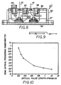
- the schematic diagram of the module 50 is shown in Figure 9.
- An isolated light-triggered thyristor module 50 can be designed according to the above description. It can have a rated blocking voltages of up to 1400 volts and average currents of 90 amperes.
- the module can be gated, for example, on with an inexpensive Gallium Arsenide (GaAs) laser diode emitting infrared radiation at a wavelength of 904 nanometers.
- GaAs Gallium Arsenide
- a glass-passivated, 16 mm diameter semiconductor body 18 can be soldered to a metallized beryllium-oxide (BeO) anode member 28, which provides the electrical isolation between the semiconductor body 18 and base plate 30.
- Anode member 28 is, in turn, soldered to base plate 30. This structure provides a low thermal impedance between the semiconductor element and external heat sink for efficient cooling of semiconductor body 18.
- BeO beryllium-oxide
- Cathode conductive layer 21 of the semiconductor body 18 provides electrical contact to cathode contact 20 of housing 11 in addition to allowing access to the optical gate 14.
- the connector 15 is mounted on the side of module 50 and the internal fiber optic light guide is bent through a 90° angle to facilitate communication to the optical gate 14 of the thyristor in the semiconductor body 18.
- the fiber optic light locator 54 is positioned adjacent optical gate 14 of the thyristor in the semiconductor 18 by means of a transparent epoxy with an index of refraction matching that of optical fiber 12. Termination of the pn junctions is accomplished by a double-sided, deep moat 46 forming a double negative bevel structure which is filled with a glass coating 38 for passivation and mechanical support.
- the entire module is filled with two electrically insulating materials such as a soft gel epoxy 47A and a hard epoxy 47B to immobilize and protect the individual components.
- Table 1 lists typical operating characteristics of a module 50.
- the effects of optical pulse length, pulse power, and anode voltage on the turn-on characteristics can also be determined.
- the average minimum optical triggering power, P LT required to turn-on the thyristor (at an anode voltage of 40V) is plotted in Figure 10 as a function of the light pulse length for several thyristors. As indicated by the curve, P LT decreases monotonically with increasing light pulse length to approximately 0.150 W.
- the E LT which is the integral of P LT *t, increased by only 20% over this range of pulse lengths.
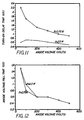
- the turn-on delay was measured from the onset of the optical pulse to 90% of V D and t F was measured from 90% V D to 10% V D .
- the higher optical power of 2.3 W is approximately 3*P LT .
- the t D is seen to decrease with increasing V D at low optical gate drives. At higher optical gate drives, however, t D is increased beyond 200 V. For the most part, t F decreases with increasing V D and is independent of the optical gate drive, as one would expect.
Landscapes
- Physics & Mathematics (AREA)
- General Physics & Mathematics (AREA)
- Optics & Photonics (AREA)
- Thyristors (AREA)
Applications Claiming Priority (2)
| Application Number | Priority Date | Filing Date | Title |
|---|---|---|---|
| US6777887A | 1987-06-29 | 1987-06-29 | |
| US67778 | 1987-06-29 |
Publications (2)
| Publication Number | Publication Date |
|---|---|
| EP0297802A2 true EP0297802A2 (de) | 1989-01-04 |
| EP0297802A3 EP0297802A3 (de) | 1990-05-23 |
Family
ID=22078356
Family Applications (1)
| Application Number | Title | Priority Date | Filing Date |
|---|---|---|---|
| EP88305818A Withdrawn EP0297802A3 (de) | 1987-06-29 | 1988-06-27 | Isoliertes lichtzündbares Thyristor-Modul |
Country Status (1)
| Country | Link |
|---|---|
| EP (1) | EP0297802A3 (de) |
Family Cites Families (3)
| Publication number | Priority date | Publication date | Assignee | Title |
|---|---|---|---|---|
| JPS5710959A (en) * | 1980-06-23 | 1982-01-20 | Mitsubishi Electric Corp | Semiconductor device |
| JPS583281A (ja) * | 1981-06-30 | 1983-01-10 | Toshiba Corp | 光駆動形半導体装置 |
| JPS58157160A (ja) * | 1982-03-12 | 1983-09-19 | Toshiba Corp | 光駆動型半導体装置 |
-
1988
- 1988-06-27 EP EP88305818A patent/EP0297802A3/de not_active Withdrawn
Also Published As
| Publication number | Publication date |
|---|---|
| EP0297802A3 (de) | 1990-05-23 |
Similar Documents
| Publication | Publication Date | Title |
|---|---|---|
| US3304429A (en) | Electrical chopper comprising photo-sensitive transistors and light emissive diode | |
| KR900003069B1 (ko) | 고체 릴레이 및 이를 제조하는 방법 | |
| US3840889A (en) | Laser diode package formed of ceramic and metal materials having high electrical and thermal conductivity | |
| US4899204A (en) | High voltage switch structure with light responsive diode stack | |
| US6111454A (en) | Power supply circuit | |
| US4825081A (en) | Light-activated series-connected pin diode switch | |
| EP0048146B1 (de) | Optisch gekoppelter Festkörper-Schalter | |
| US4240088A (en) | Semiconductor high-voltage switch | |
| US4122479A (en) | Optoelectronic device having control circuit for light emitting element and circuit for light receiving element integrated in a semiconductor body | |
| US3925801A (en) | Photon isolator with improved photodetector transistor stage | |
| US4110781A (en) | Bidirectional grooved thyristor fired by activation of the beveled surfaces | |
| US4450461A (en) | Low cost high isolation voltage optocoupler with improved light transmissivity | |
| JPS5825286A (ja) | 光励起発光素子 | |
| WO1990003591A1 (en) | Dual mode light emitting diode/detector diode for optical fiber transmission lines | |
| US20190222211A1 (en) | Switching power module combining a gate driver with a photonic isolated power source | |
| US5001355A (en) | Photon energy activated radio frequency signal switch | |
| US3590344A (en) | Light activated semiconductor controlled rectifier | |
| KR100218587B1 (ko) | 사이리스터를 구비한 반도체집적회로 | |
| EP0400153A1 (de) | Optische halbleitervorrichtung mit einer nulldurchgangsfunktion | |
| US4137428A (en) | Optically actuated bidirectional semiconductor switch | |
| US4136351A (en) | Photo-coupled semiconductor device | |
| KR19990029224A (ko) | 반도체레이저장치 | |
| US6365951B1 (en) | Methods on constructing an avalanche light emitting diode | |
| US3938173A (en) | Optically coupled semiconductive switching devices | |
| US6154477A (en) | On-board laser-triggered multi-layer semiconductor power switch |
Legal Events
| Date | Code | Title | Description |
|---|---|---|---|
| PUAI | Public reference made under article 153(3) epc to a published international application that has entered the european phase |
Free format text: ORIGINAL CODE: 0009012 |
|
| AK | Designated contracting states |
Kind code of ref document: A2 Designated state(s): DE FR GB |
|
| PUAL | Search report despatched |
Free format text: ORIGINAL CODE: 0009013 |
|
| AK | Designated contracting states |
Kind code of ref document: A3 Designated state(s): DE FR GB |
|
| STAA | Information on the status of an ep patent application or granted ep patent |
Free format text: STATUS: THE APPLICATION IS DEEMED TO BE WITHDRAWN |
|
| 18D | Application deemed to be withdrawn |
Effective date: 19900703 |