EP0298486A2 - Appareil pour la détection d'une différence de phase - Google Patents
Appareil pour la détection d'une différence de phase Download PDFInfo
- Publication number
- EP0298486A2 EP0298486A2 EP88110890A EP88110890A EP0298486A2 EP 0298486 A2 EP0298486 A2 EP 0298486A2 EP 88110890 A EP88110890 A EP 88110890A EP 88110890 A EP88110890 A EP 88110890A EP 0298486 A2 EP0298486 A2 EP 0298486A2
- Authority
- EP
- European Patent Office
- Prior art keywords
- signal
- signals
- time series
- light
- section
- Prior art date
- Legal status (The legal status is an assumption and is not a legal conclusion. Google has not performed a legal analysis and makes no representation as to the accuracy of the status listed.)
- Granted
Links
- 230000004907 flux Effects 0.000 claims abstract description 4
- 239000003990 capacitor Substances 0.000 claims description 7
- 238000006243 chemical reaction Methods 0.000 abstract description 14
- 238000010586 diagram Methods 0.000 description 11
- 238000001444 catalytic combustion detection Methods 0.000 description 7
- 239000004065 semiconductor Substances 0.000 description 6
- 108091006146 Channels Proteins 0.000 description 4
- 230000003287 optical effect Effects 0.000 description 4
- 239000011295 pitch Substances 0.000 description 4
- 239000000758 substrate Substances 0.000 description 3
- VYPSYNLAJGMNEJ-UHFFFAOYSA-N Silicium dioxide Chemical compound O=[Si]=O VYPSYNLAJGMNEJ-UHFFFAOYSA-N 0.000 description 2
- 238000006073 displacement reaction Methods 0.000 description 2
- 238000000034 method Methods 0.000 description 2
- 229910021420 polycrystalline silicon Inorganic materials 0.000 description 2
- 229920005591 polysilicon Polymers 0.000 description 2
- 244000182067 Fraxinus ornus Species 0.000 description 1
- 230000004888 barrier function Effects 0.000 description 1
- 229910052681 coesite Inorganic materials 0.000 description 1
- 238000010276 construction Methods 0.000 description 1
- 229910052906 cristobalite Inorganic materials 0.000 description 1
- 238000001514 detection method Methods 0.000 description 1
- 238000009792 diffusion process Methods 0.000 description 1
- 238000005036 potential barrier Methods 0.000 description 1
- 230000004044 response Effects 0.000 description 1
- 239000000377 silicon dioxide Substances 0.000 description 1
- 235000012239 silicon dioxide Nutrition 0.000 description 1
- 229910052682 stishovite Inorganic materials 0.000 description 1
- 229910052905 tridymite Inorganic materials 0.000 description 1
Images


Classifications
-
- G—PHYSICS
- G02—OPTICS
- G02B—OPTICAL ELEMENTS, SYSTEMS OR APPARATUS
- G02B7/00—Mountings, adjusting means, or light-tight connections, for optical elements
- G02B7/28—Systems for automatic generation of focusing signals
- G02B7/34—Systems for automatic generation of focusing signals using different areas in a pupil plane
Definitions
- the present invention relates to a phase difference detecting apparatus which is suitably applicable, for example, to an automatic focal point detecting device of a camera, and particularly relates to a phase difference detecting apparatus for performing operation processing for phase difference detection through analog signal processing.
- a convention phase difference detecting apparatus will be described in relation to an automatic focal point detecting device of a camera.
- a condenser lens, a separator lens and a phase difference detecting apparatus are positioned in order in the rear of a film equivalent plane located in the rear of an objective lens.
- the phase difference detecting apparatus is provided with a pair of image sensors constituted by CCDs or the like for photoelectrically converting a pair of subject images focused by the separator lens, and an operation circuit for operating on a phase difference between the pair of subject images on the basis of electric signals generated through the photoelectric conversion so as to judge the focus state.
- a signal B(k) to be operated on which is time-serially output from one of the image sensors and a signal R(k) to be operated on which is time-serially output from the other image sensor are subject to differential operation on the basis of the following equation (1) to thereby calculate values H(1), H(2) H(l), so that the focus state and the quantity of focal displacement are detected on the basis of a distribution pattern of the correlative values.
- H(l
- phase difference detecting apparatus In such a conventional phase difference detecting apparatus, however, there have been problems in that since operation is carried out through digital signal processing by using a micro-computer or the like, an expensive A/D converter and so on are required in order to perform the high-speed and accurate operation, round off errors are produced due to limitation in the number of bits of the microcomputer or the like for carrying out the operation so that the accuracy of the operation deteriorates, the work of design of computer programming for the operation processing becomes large, a memory capable of storing a great number of digital data is required, and so on.
- the phase difference detecting apparatus for detecting a relative distance between a pair of focused images obtained from subject luminous flux passed through an objective lens to thereby judge a focusing state of the objective lens, comprises: a first light receiving section constituted by picture elements arranged in a row so as to receive a first one of the focused images; a first signal reading-out section for transferring, in a predetermined direction, signals generated in the respective picture elements of the first light receiving section and at the same time outputting the signals in parallel to each other through floating gates of a CCD; a first signal generating means including the first light receiving means, the first signal reading-out means, and means for converting the signals output in parallel from the first signal reading-out section into a first time series signal and outputting the first time series signal; a second light receiving section constituted by picture elements arranged in a row to receive a second one of the focused images; a second signal reading-out section for transferring, in a predetermined direction, signals generated in the respective
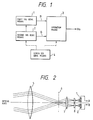
- Fig. 1 is a block diagram illustrating a basic arrangement which is constituted by first and second signal generating means 1 and 2 for respectively generating a pair of signals R and B to be operated on a phase difference between which is to be detected, an operation means 3 for performing the same processing of differential operation as the above-mentioned equation (1), and a synchronizing signal- generating means 4 for controlling the operation of the entire apparatus.
- phase difference detecting apparatus may be applied to various usages since it is generally capable of detecting a phase difference between a pair of signals to be operated on, the embodiment will be described as to a case in which the phase difference detecting apparatus is applied to an automatic focal point detecting device of a camera for photography, for a video system, or the like.
- a condenser lens 7 and a separator lens 8 are disposed in the rear of a film equivalent plane 6 which is in turn disposed in the rear of an objective lens 5 provided in an optical system of a camera, and a first and a second signal generating menas 1 and 2 are provided in a focal plane of the separator lens 8.
- Fig. 3 shows the case where a reference image sensor and a reference reading-out section and a base image sensor and a base reading-out section disclosed in No. 61-222211 are used as the first signal generating means 1 and the second signal generating means 2, respectively.
- the first signal generating means 1 includes a light receiving section 22 having a plurality of photoelectric conversion elements constituted by photodiodes D r1 - D rn for receiving one of the focused images from the separator lens 8
- the second signal generating means 2 includes a light receiving section 23 having a plurality of photoelectric conversion elements constituted by photodiodes D b1 - D bn for receiving the other focused image from the separator lens 8.
- the light receiving sections 22 and 23 are separated from each other by a predetermined distance and extended in the direction perpendicular to the optical axis.
- a storage section 24 and a shift register section 26 are successively provided to follow the light receiving section 22 and a storage section 25 and a shift register section 27 are successively provided to follow the light receiving section 23.
- the storage section 24 and the shift register section 26 are constituted by CCDs (charge transfer devices) respectively including charge transfer elements T r1 - T rn and C r1 - C rn respectively corresponding to the photoelectric conversion elements D r1 - D rn
- the storage section 25 and the shift register section 27 are constituted by CCDs respectively including charge transfer elements T b1 - T bn and C b1 - C bn respectively corresponding to the photoelectric conversion elements D b1 - D bn .
- the storage section 24 receives in parallel signal charges generated in the conversion elements D r1 - D rn and transfers in parallel the received signal charges to the shift register section 26, while storage section 25 receives in parallel signal charges generated in the conversion elements D b1 - D bn and transfers in parallel the received signal charges to the shift register section 27.
- the one shift register section 26 transfers the charges in the horizontal direction as indicated by an arrow. Although the operation of the shift register sections 26 and 27 will be described later, the other shift register section 27 is arranged so as not to transfer the charges in the horizontal direction.
- the reference numerals 28 and 29 represent conductive layers which are formed on the surfaces of channel sections for transferring the signal charges from the light receiving sections 22 and 23 to the storage sections 24 and 25 respectively.
- the conductive layers are formed of polysilicon layers to act as potential barriers respectively.
- the reference numerals 30 and 31 represent transfer gates 30 and 31 for controlling the movement of the signal charges respectively.
- floating gates F r1 - F rn are formed adjacently to the charge transfer elements C r1 - C rn respectively, and are connected to a reset terminal RES through MOS FETs M r1 - M rn each having a gate supplied with a control signal CE and to a common connection point Pr through MOS FETs Q r1 - Q rn for performing multiplex operation to channel change-over signals CH 1 - CH n applied to their gates.
- floating gates F b1 - F bn are fomred adjacently to the charge transfer elements C b1 - C bn respectively, and are connected to a reset terminal RES through MOS FETs M b1 - M bn each having a gate supplied with a control signal CE and to a common connection point Pb through MOS FETs Q b1 - Q bn for performing multiplex operation in response to channel change-over signals CH 1 - CH n applied to their gates.
- the connection points are connected to output terminals P ro and P bo through impedance conversion circuits 32 and 33 respectively.
- the impedance conversion circuits 32 and 33 have the same construction as each other.
- the circuit 32 is constituted by MOS FETs I r1 and I r2 with their drain-source circuits connected in series to each other between a power source V DD and an earth terminal, and an MOS FET I r3 connected in parallel to the gate-source circuit of the MOS FET I r1 for clamping the common connection point Pr to the power source V DD upon application of a refresh signal ⁇ R
- the circuit 33 is constituted by MOS FETs I b1 and I b2 with their drain-source circuits connected in series to each other between the power source V DD and the earth terminal, and an MOS FET I b3 connected in parallel to the gate-source circuit of the MOS FET I b1 for clamping the common connection point Pb to the power source VDD upon application of a refresh signal ⁇ R .
- the gate of each of the MOS FETs I r2 and I b2 is biased to a pre
- each of hte set of photoelectric conversion elements constituting the light receiving section 22 and the set of charge transfer elements constituting each of the storage section 24 and the shift register sectuion 26 is forty-eight in number.
- the forty-eight elements in each set are provided at equal pitch widths W and grouped into a first, a second and a third block I R , II R and III R , the four elememts located at one side belonging to the first block I R , the four elements located at the other side belonging to the second block II R , the remainder 40 elements belonging to the third block III R .
- the floating gates F r1 - F r40 are provided correspondingly to the charge transfer elements C r1 - C r40 belonging to the third block III R and grouped into a fourth and a fifth block IV R and V R including the thirty-two floating gates F r1 - F r32 and the remainder eight floating gates respectively.
- the respective one ends of the forty floating gates F r1 - F r40 are connected to the reset termial RES through the MOS FETs M r1 , M r2 , ..., and the floating gates F r1 - F r32 of them are connected commonly to the connection point Pr through the MOS FETs Q r1 - Q rn , as seen in Fig. 3. That is, only the parts belonging to the third and fourth blocks III R and IV R of Fig. 4 are illustrated as the representative in the first signal generating means 1 in Fig. 3, while the parts belonging to the other blocks I R , II R and V R which are the preparatory areas to be actuated to transfer the signal charges in the horizontal direction are omitted in Fig. 3.
- each of the set of photoelectric conversion elements constituting the light receiving section 23 and the set of charge transfer elements constituting each of the storage section 25 and the shift register section 27 is forty in number.
- the forty elements in each set are provided at equal pitch widths W (equal to those in the first signal generating means 1) and grouped into a first, a second and a third block I R , II B and III B , the four elements located at one side belonging to the first block I B , the four elements located at the other side belonging to the second block II B , the remainder 32 elements belonging to the third block III R .
- the floating gates F b1 - F b32 are provided correspondigly to the charge transfer elements C b1 - C b32 belonging to the third block III B .
- the respective one ends of the floating gates F b1 - F b32 are connectede to the MOS FETs M b1 - M bn and Q b1 - Q bn in Fig. 3. That is, the second signal generating means is illustrated in Fig. 3 as to the third block III B of Fig. 4.
- the phase difference detecting apparatus is constituted by an IC as a semiconductor integrated circuit device, and the structures of the signal generating means 1 and 2 and the floating gates shown in Figs. 3 and 4 will be described with reference to a schematic sectional view of Fig. 5.
- a plurality of N+-type layers are formed in a portion of a P-type diffusion layer (P-well) formed in a surface portion of an N-type semiconductor substrate to thereby form the photoelectric conversion elements of the light receiving section 22(23).
- Transfer gate electrode layers constituting the respective charge transfer elements of the barrier section 28 (29) and the storage section 24 (25), a gate electrode layer constituting the transfer gate 30 (31), and transfer gate electrode layers constituting the respective charge transfer elements of the shift register section 26 (27) are provide side by side on the semiconductor substrate through an SiO2 layer (not shown).
- an electrode layer Al to be clamped to the power source V DD and polysilicon layers constituting the floating gates F r1 - F rn and F b 1 - F bn are laminated adjacently to the shift register section 26 (27).
- the electrode layer Al is formed to cover the whole of the upper surfaces of the floating gates F r1 - F rn and F b1 - F bn formed in plurality.
- the MOS FETs M r1 - M rn and M r1 - M rn are connected to the one ends of the respective floating gates.
- the potential of a resent signal ⁇ FG applied to the reset terminal RES is made equal to the power source V DD and te floating gates F r1 - F rn (F b1 - F bn ) are clamped to the poewer source V DD through the MOS FETs M r1 - M rn (M b1 - M bn ) by a "H"-level control signal CE. If the MOS FETs M r1 - M rn (M b1 - M bn ) are then turned off again, a deep potential well is formed in the semiconductor substrate as indicated by a dotted line in Fig.
- the signals thus generated through the floating gates F r1 - F rn (F b1 - F bn ) are converted into a time series signal R(k) (B(k)) by the multiplex operation of the MOS FETs Q r1 - Q rn (Q b1 - Q bn ), and the time series signal R(k) (B(K)) are output to the output terminal P rO (P bO ).
- the operation means 3 is constituted by a switching-capacitor integrator.
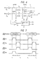
- a signal line extended from the output terminal P rO of the first signal generating means 1 (with reference to Fig. 3) is connected to an inversion input terminal of a differential integrator 42 through a series connection of a switching element 40, a capacitive element C s1 , and a switching element 41, the opposite ends of the capacitive element C s1 being connected to an earth terminal through switching elements 43 and 44 respectively.
- a signal line extended from the output terminal P bO of the second signal generating means 2 (with reference to Fig.
- inversion and non-inversion input terminals of an analog comparator 51 are respectively connected to the signal lines extended from the output terminals P rO and P bO , and an output terminal of the analog comparator 51 is connected to an input terminal of a channel selection circuit 52 which generates selection signals ⁇ 1, ⁇ 2, KA and KB for controlling "ON” and “OFF” of the switching elements 40, 41, 43, 44, 45, 46, 47 and 48.
- the analog comparator 51 outputs a polarity signal S gn which has an "H"-level when the levels of the signals to be operated are in the relationship of R(k) ⁇ B(k) and has an "L"-level when R(k) ⁇ B(k), so that the voltage levels of the selection signals ⁇ 1, ⁇ 2, KA and KB are determined on the basis of the level of the polarity signal S gn .
- the signals R(k) and B(k) to be operated on are output, respectively, from the first and second signal generating means 1 and 2 with a predetermined period as shown in the diagram (A) of Fig. 7.
- the signals to be operated on are in the relationship of R(k) ⁇ B(k), for example, in a period from a point of time t1 to a point of time t2, the polarity signal S gn becomes "H" so that the selection signals ⁇ 1, ⁇ 2, KA and KB of rectangular waves as shown in the respective diagrams (B), (C), (D) and (E) of Fig. 7 are generated.
- the selection signals ⁇ 1 and ⁇ 2 are generated in a timing so that both of the signals KA and KB do not become "H" simultaneously. If the signals to be operated are in the relationship of R(k) ⁇ B(k), for example, in a period from a point to time t3 to a point of time t4, on the other hand, the polarity signal S gn beocmes "L" so that the selection signals KA and KB whose phases are opposite to those in the period from the point of time t1 to the point of time t2.
- the selection signals ⁇ 1 and ⁇ 2 are generated in a constant timing independently of the level of the polarity signal S gn .
- the switching elements 44, 48, 40 and 47 are made to be "ON" by those selection signals ⁇ 1, ⁇ 2, KA and KB in a fore-half period T F1 of the period t1 - t2 so that the capacitive element C S1 is charged with the signal R(k) to be operated while the unnecessary charges of the capacitive element C S2 are discharged.
- the switching elements 44, 48, 43 and 45 are "ON" in a fore-half period T F2 of the period t3 - t4 so that the capacitive element C S2 is charged with the signal B(k) to be operated on and the unnecessary charges of the capacitive element C S1 are discharged.
- the signal charges held by the shift register section 26 of the first signal generating means 1 are transferred by a part corresponding to one pitch to the signal charges of the other shift register section 27, and the signal charges of the respective shift register sections 26 and 27 which are displaced in phase relative to each other are time serially read out again so as to be subject to the operation processing of the above equation (4).
- the signal charges of the shift register sections 26 and 27 are displaced in phase relative to each other and subject to the processing repeatedly.
- the displacement in phase corresponds to the above-mentioned quantity of relative movement l, and the correlative value when the quantity of movement l is sequentially changed can be obtained as the following equation (5) and can be detected as a voltage signal from the output terminal 49.
- this equation (5) corresponds to the above-mentioned equation (1), and the correlative values H(1), H(2)..., H(l) can be obtained through analog signal processing.
- the phase difference can be detected on the basis of a pattern of distribution of these correlative values.
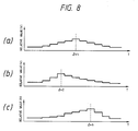
- the diagrams (a) - (c) of Fig. 8 show the patterns of the correlative values in the case where the apparatus is applied to an automatic focal-point detecting device in a camera. Assuming that the state in focus is obtained in the case of the diagram (a) of Fig.
- phase difference detecting apparatus in which a relative distance between a pair of focused images obtained from subject luminous flux passed through a taking lens is detected to thereby judge the state of focus of the taking lens
- signals generated by photoelectric conversion of the respective focused images are stored in CCDs and are non-destructively output through floating gates provided on the CCDs, so that it is not necessary to separately provide a large-scale memory to make it possible to reduce the size of the apparatus.
- the method of charge-couple by means of capacitive elements is used to calculate the correlative values of the output signals, it is possible to perform the operation at a high speed and accurately.
- the phase difference detecting apparatus according to the present invention can be suitably produced in the form of a semiconductor integrated circuit.
Landscapes
- Physics & Mathematics (AREA)
- General Physics & Mathematics (AREA)
- Optics & Photonics (AREA)
- Focusing (AREA)
- Automatic Focus Adjustment (AREA)
Applications Claiming Priority (2)
| Application Number | Priority Date | Filing Date | Title |
|---|---|---|---|
| JP62167906A JPH0810297B2 (ja) | 1987-07-07 | 1987-07-07 | 位相差検出装置 |
| JP167906/87 | 1987-07-07 |
Publications (3)
| Publication Number | Publication Date |
|---|---|
| EP0298486A2 true EP0298486A2 (fr) | 1989-01-11 |
| EP0298486A3 EP0298486A3 (en) | 1989-06-14 |
| EP0298486B1 EP0298486B1 (fr) | 1993-10-06 |
Family
ID=15858242
Family Applications (1)
| Application Number | Title | Priority Date | Filing Date |
|---|---|---|---|
| EP88110890A Expired - Lifetime EP0298486B1 (fr) | 1987-07-07 | 1988-07-07 | Appareil pour la détection d'une différence de phase |
Country Status (4)
| Country | Link |
|---|---|
| US (1) | US5008696A (fr) |
| EP (1) | EP0298486B1 (fr) |
| JP (1) | JPH0810297B2 (fr) |
| DE (1) | DE3884685T2 (fr) |
Cited By (2)
| Publication number | Priority date | Publication date | Assignee | Title |
|---|---|---|---|---|
| EP0459484A3 (en) * | 1990-05-30 | 1992-09-23 | Fuji Photo Film Co., Ltd. | Automatic focusing system with phase difference detecting unit employing correlation operating circuit |
| FR2676552A1 (fr) * | 1991-05-15 | 1992-11-20 | Asahi Optical Co Ltd | Dispositif de mise au point automatique. |
Families Citing this family (3)
| Publication number | Priority date | Publication date | Assignee | Title |
|---|---|---|---|---|
| JP3832441B2 (ja) | 2002-04-08 | 2006-10-11 | 松下電工株式会社 | 強度変調光を用いた空間情報の検出装置 |
| US7461790B2 (en) * | 2006-04-04 | 2008-12-09 | Datalogic Scanning, Inc. | Data reader and methods for imaging targets exposed to high intensity illumination |
| CN120970816B (zh) * | 2025-10-20 | 2026-02-03 | 杭州高谱成像技术有限公司 | 一种实时自动对焦的高光谱采集方法及装置 |
Family Cites Families (12)
| Publication number | Priority date | Publication date | Assignee | Title |
|---|---|---|---|---|
| JPS51142318A (en) * | 1975-05-20 | 1976-12-07 | Asahi Optical Co Ltd | Focus adjusting device for optical systems |
| JPS5385454A (en) * | 1977-01-06 | 1978-07-27 | Canon Inc | Distance detecting method |
| DE2801383A1 (de) * | 1978-01-13 | 1979-07-19 | Agfa Gevaert Ag | Fotografische kamera mit einer fokussiervorrichtung |
| JPS54161355A (en) * | 1978-06-09 | 1979-12-20 | Minolta Camera Co Ltd | Automatic range finder |
| JPS558102A (en) * | 1978-07-03 | 1980-01-21 | Olympus Optical Co Ltd | Picture signal process circuit |
| US4470676A (en) * | 1978-07-28 | 1984-09-11 | Canon Kabushiki Kaisha | Focus detecting device |
| JPS55111921A (en) * | 1979-02-14 | 1980-08-29 | Asahi Optical Co Ltd | Focus detector of camera |
| JPS55115023A (en) * | 1979-02-28 | 1980-09-04 | Canon Inc | Distance detector and focus control system utilizing this |
| DE2936491A1 (de) * | 1979-09-10 | 1981-05-21 | Siemens AG, 1000 Berlin und 8000 München | Mit einem belichtungsmessteil versehene schaltung zur sensorgesteuerten entfernungsmessung |
| JPS57161839A (en) * | 1981-03-31 | 1982-10-05 | Canon Inc | Distance measuring device of camera |
| JPS59208513A (ja) * | 1983-05-12 | 1984-11-26 | Canon Inc | 焦点検出装置 |
| US4709138A (en) * | 1984-02-09 | 1987-11-24 | Canon Kabushiki Kaisha | Apparatus for detecting shake of image of object |
-
1987
- 1987-07-07 JP JP62167906A patent/JPH0810297B2/ja not_active Expired - Fee Related
-
1988
- 1988-07-07 US US07/216,354 patent/US5008696A/en not_active Expired - Lifetime
- 1988-07-07 EP EP88110890A patent/EP0298486B1/fr not_active Expired - Lifetime
- 1988-07-07 DE DE88110890T patent/DE3884685T2/de not_active Expired - Fee Related
Cited By (7)
| Publication number | Priority date | Publication date | Assignee | Title |
|---|---|---|---|---|
| EP0459484A3 (en) * | 1990-05-30 | 1992-09-23 | Fuji Photo Film Co., Ltd. | Automatic focusing system with phase difference detecting unit employing correlation operating circuit |
| US5359383A (en) * | 1990-05-30 | 1994-10-25 | Fuji Photo Film Co., Ltd. | Automatic focusing system with phase difference detecting unit employing correlation operating circuit |
| FR2676552A1 (fr) * | 1991-05-15 | 1992-11-20 | Asahi Optical Co Ltd | Dispositif de mise au point automatique. |
| US5448329A (en) * | 1991-05-15 | 1995-09-05 | Asahi Kogaku Kogyo Kabushiki Kaisha | Focus detecting apparatus for determining whether an object is moving |
| US5612761A (en) * | 1991-05-15 | 1997-03-18 | Asahi Kogaku Kogyo Kabushiki Kaisha | Automatic focusing apparatus |
| US5640225A (en) * | 1991-05-15 | 1997-06-17 | Asahi Kogaku Kogyo Kabushiki Kaisha | Backlash compensation for automatic focusing apparatus |
| US5664239A (en) * | 1991-05-15 | 1997-09-02 | Asahi Kogaku Kogyo Kabushiki Kaisha | Automatic focusing apparatus |
Also Published As
| Publication number | Publication date |
|---|---|
| JPS6413110A (en) | 1989-01-18 |
| JPH0810297B2 (ja) | 1996-01-31 |
| EP0298486B1 (fr) | 1993-10-06 |
| EP0298486A3 (en) | 1989-06-14 |
| DE3884685D1 (de) | 1993-11-11 |
| DE3884685T2 (de) | 1994-01-27 |
| US5008696A (en) | 1991-04-16 |
Similar Documents
| Publication | Publication Date | Title |
|---|---|---|
| US4521106A (en) | Image sensor and rangefinder device with background subtraction using interlaced analog shift register | |
| US4490036A (en) | Image sensor and rangefinder device having background subtraction with paired analog shift registers | |
| US4490037A (en) | Image sensor and rangefinder device having background subtraction with bridge network | |
| US4740681A (en) | Star sensor for attitude detection of a spinning satellite | |
| EP0280511A2 (fr) | Caméra vidéo pour image fixe | |
| JPS6251550B2 (fr) | ||
| US5539536A (en) | Linear imaging sensor having improved charged transfer circuitry | |
| US5917960A (en) | Image correlator, an image processing apparatus using the same, and a signal adder used in the image correlator | |
| US4609825A (en) | Device for modulating the sensitivity of a line-transfer photosensitive device | |
| EP0298486A2 (fr) | Appareil pour la détection d'une différence de phase | |
| US3952290A (en) | Read-only optical memory system | |
| AU603159B2 (en) | Ccd image sensor arrangement | |
| US4575626A (en) | Apparatus for detecting focus conditions of an imaging optical system | |
| US4945377A (en) | Phase difference detecting apparatus | |
| US5068738A (en) | Phase-difference detector using an analog arithmetic correlation device | |
| US4959726A (en) | Automatic focusing adjusting device | |
| US4866528A (en) | Image pickup apparatus providing lessened flicker in electronic still cameras and the like | |
| EP0820030B1 (fr) | Logique de calcul a semi-conducteur | |
| US4849619A (en) | Phase difference detector with analog signals | |
| EP0200270A1 (fr) | Dispositif à couplage de charge et caméra comportant un tel dispositif | |
| US4833636A (en) | Analog, two signal correlator | |
| US5285234A (en) | Phase difference detecting type autofocusing device including an optical system having first and second lenses | |
| US4926205A (en) | Phase-difference detector | |
| JP2001112026A (ja) | 3次元画像検出装置 | |
| JPS5911303B2 (ja) | 固体撮像素子の信号処理方法 |
Legal Events
| Date | Code | Title | Description |
|---|---|---|---|
| PUAI | Public reference made under article 153(3) epc to a published international application that has entered the european phase |
Free format text: ORIGINAL CODE: 0009012 |
|
| AK | Designated contracting states |
Kind code of ref document: A2 Designated state(s): DE FR GB |
|
| PUAL | Search report despatched |
Free format text: ORIGINAL CODE: 0009013 |
|
| AK | Designated contracting states |
Kind code of ref document: A3 Designated state(s): DE FR GB |
|
| 17P | Request for examination filed |
Effective date: 19891017 |
|
| 17Q | First examination report despatched |
Effective date: 19911031 |
|
| GRAA | (expected) grant |
Free format text: ORIGINAL CODE: 0009210 |
|
| AK | Designated contracting states |
Kind code of ref document: B1 Designated state(s): DE FR GB |
|
| REF | Corresponds to: |
Ref document number: 3884685 Country of ref document: DE Date of ref document: 19931111 |
|
| ET | Fr: translation filed | ||
| PLBE | No opposition filed within time limit |
Free format text: ORIGINAL CODE: 0009261 |
|
| STAA | Information on the status of an ep patent application or granted ep patent |
Free format text: STATUS: NO OPPOSITION FILED WITHIN TIME LIMIT |
|
| 26N | No opposition filed | ||
| REG | Reference to a national code |
Ref country code: GB Ref legal event code: IF02 |
|
| PGFP | Annual fee paid to national office [announced via postgrant information from national office to epo] |
Ref country code: GB Payment date: 20040707 Year of fee payment: 17 |
|
| PGFP | Annual fee paid to national office [announced via postgrant information from national office to epo] |
Ref country code: FR Payment date: 20040708 Year of fee payment: 17 |
|
| PGFP | Annual fee paid to national office [announced via postgrant information from national office to epo] |
Ref country code: DE Payment date: 20040715 Year of fee payment: 17 |
|
| PG25 | Lapsed in a contracting state [announced via postgrant information from national office to epo] |
Ref country code: GB Free format text: LAPSE BECAUSE OF NON-PAYMENT OF DUE FEES Effective date: 20050707 |
|
| PG25 | Lapsed in a contracting state [announced via postgrant information from national office to epo] |
Ref country code: DE Free format text: LAPSE BECAUSE OF NON-PAYMENT OF DUE FEES Effective date: 20060201 |
|
| GBPC | Gb: european patent ceased through non-payment of renewal fee |
Effective date: 20050707 |
|
| PG25 | Lapsed in a contracting state [announced via postgrant information from national office to epo] |
Ref country code: FR Free format text: LAPSE BECAUSE OF NON-PAYMENT OF DUE FEES Effective date: 20060331 |
|
| REG | Reference to a national code |
Ref country code: FR Ref legal event code: ST Effective date: 20060331 |