EP0299251A2 - Filtre de communication - Google Patents
Filtre de communication Download PDFInfo
- Publication number
- EP0299251A2 EP0299251A2 EP88110022A EP88110022A EP0299251A2 EP 0299251 A2 EP0299251 A2 EP 0299251A2 EP 88110022 A EP88110022 A EP 88110022A EP 88110022 A EP88110022 A EP 88110022A EP 0299251 A2 EP0299251 A2 EP 0299251A2
- Authority
- EP
- European Patent Office
- Prior art keywords
- signal
- symbol
- signals
- generating
- gate
- Prior art date
- Legal status (The legal status is an assumption and is not a legal conclusion. Google has not performed a legal analysis and makes no representation as to the accuracy of the status listed.)
- Granted
Links
- 238000004891 communication Methods 0.000 title abstract description 14
- 238000000034 method Methods 0.000 claims abstract description 10
- 238000001514 detection method Methods 0.000 claims description 23
- 238000006243 chemical reaction Methods 0.000 claims 1
- 230000007704 transition Effects 0.000 abstract description 6
- 230000005540 biological transmission Effects 0.000 abstract description 5
- 230000000644 propagated effect Effects 0.000 abstract description 4
- 238000010586 diagram Methods 0.000 description 7
- 230000000295 complement effect Effects 0.000 description 2
- 239000000945 filler Substances 0.000 description 2
- 238000012546 transfer Methods 0.000 description 2
- 239000004614 Process Aid Substances 0.000 description 1
- 230000002457 bidirectional effect Effects 0.000 description 1
- 230000015556 catabolic process Effects 0.000 description 1
- 238000006731 degradation reaction Methods 0.000 description 1
- 238000013461 design Methods 0.000 description 1
- 238000002955 isolation Methods 0.000 description 1
- 230000006855 networking Effects 0.000 description 1
- 239000013307 optical fiber Substances 0.000 description 1
- 230000002265 prevention Effects 0.000 description 1
- 230000008569 process Effects 0.000 description 1
- 230000000750 progressive effect Effects 0.000 description 1
- 230000004044 response Effects 0.000 description 1
- 230000008054 signal transmission Effects 0.000 description 1
- 230000001360 synchronised effect Effects 0.000 description 1
- 230000009897 systematic effect Effects 0.000 description 1
- 238000012360 testing method Methods 0.000 description 1
Images

Classifications
-
- H—ELECTRICITY
- H04—ELECTRIC COMMUNICATION TECHNIQUE
- H04J—MULTIPLEX COMMUNICATION
- H04J3/00—Time-division multiplex systems
- H04J3/02—Details
- H04J3/06—Synchronising arrangements
- H04J3/062—Synchronisation of signals having the same nominal but fluctuating bit rates, e.g. using buffers
- H04J3/0632—Synchronisation of packets and cells, e.g. transmission of voice via a packet network, circuit emulation service [CES]
-
- H—ELECTRICITY
- H04—ELECTRIC COMMUNICATION TECHNIQUE
- H04L—TRANSMISSION OF DIGITAL INFORMATION, e.g. TELEGRAPHIC COMMUNICATION
- H04L12/00—Data switching networks
- H04L12/28—Data switching networks characterised by path configuration, e.g. LAN [Local Area Networks] or WAN [Wide Area Networks]
- H04L12/42—Loop networks
- H04L12/427—Loop networks with decentralised control
- H04L12/433—Loop networks with decentralised control with asynchronous transmission, e.g. token ring, register insertion
Definitions
- European application 85 309 199.9 and European application 85 309 200.5 of the instant applicant.
- the invention relates to the transmission of signals onto a telecommunications network and, more particularly, to the detection of spurious signals and the prevention of false connection to the network.
- Interconnection in a network of electronic equipment is typically governed by standard data "protocols" which specify how a particular node in the network will receive and transmit information over the network.
- This information is generally contained in "packets" having a definite format and a packet is preceded and terminated by special symbols for ease of recognition.
- Connection management procedures are designed to recognise these special symbols and to initiate proper connection to the network. The procedures should avoid false connection as well as detect the presence of spurious signals on the network. Generation of spurious signals on the network is obviously an important problem.
- Spurious signals can arise from excessive noise on the network.
- nodes on the network act as “repeaters”. That is they receive signal packets, decode them, encode them and transmit them to another node.
- Spurious symbols received should, accordingly, be detected and not propagated. This detection process aids in the isolation of faulty nodes. Additionally, these noisy symbols could be misinterpreted as connection management symbols and could falsely initiate connection of a node to the network.
- a portion of a packet may have a parity error which could also be misinterpreted.
- improper symbols such as noisy symbols or those with a parity error
- a communications management unit employing a circuit according to the invention would, upon reception of an improper symbol, cause the transmission of symbols to halt.
- improper symbols are not propagated on the network by a node employing the instant invention.
- false interconnections are avoided and noisy symbols, which might be misinterpreted are eliminated.
- faulty nodes within the network can be isolated.
- the invention is described in terms of a state machine having three states.
- ENDEC On reset, ENDEC is in "through" state, (first state). Reception in the first state of any improper symbol, halt (H), quiet (Q), violation (V), isolated J, isolated K, or any symbol with a parity error, causes entry into a second (forced halt) state. Any proper symbol received in the first state is transmitted. An IDLE symbol received when in state one, causes transition to a third (forced idle) state. Return to the reset state is accomplished by reception of a JK symbol-pair. Apparatus implementing the three-state machine of the instant invention is disclosed.
- Fig. 1 illustrates the typical manner of utilizing a local area network node 10 to interconnect a host computer system 16 with a physical network media 34, 36.
- the node 10 will include a node controller 14, an encoder/decoder/ or ENDEC, 12 and an interface unit 18 as integral system components.
- the host computer 16 typically communicates with the node controller 14 of the node 10 over a bidirectional data bus 28.
- the node controller 14 transfers data to and from the ENDEC 12 over the data busses 24, 26, respectively.
- the node controller 14 controls and determines the status of the ENDEC 12 by means of the control bus 22.
- a system clock, 0 s y s is provided on the clock line 20 to the ENDEC 12 to ensure that the system components are properly synchronized.
- the ENDEC 12 functions to prepare the raw transmitter data provided by the node controller 14 for transmission to the interface system component 18 over the serial data bus 30 and, subsequently, onto the network media 34.
- the ENDEC 12 further functions to recover data received from the network media 36 via the interface system component 18 and the serial data bus 32. This recovered data is then transferred to the node controller 14 over the return data bus 26.
- the interface system component 18 functions to provide a physical interconnect between the node 10 and network media 34, 36.
- the interface 18 may simply be a coaxial "T" connector, for example.
- the interface may perform a more complex function.
- the media 34, 36 is an optical fiber communications cable
- the interface 18 also preferably includes an electro-optic transmitter and receiver.
- the network media 34, 36 itself is preferably only a passive single high-speed serial data bus that physically interconnects each of the nodes 10.
- the topology of the network i.e., ring, redundant loop, or linear, is thus established by how the nodes are interconnected, in terms of nearest neighbor relationships, by the physical network media.
- networking protocols There are a number of somewhat different networking protocols, or systematic procedures of operation, that may be implemented to control the overall operation of the network.
- a design choice in the assemblage of the network is the selection of one of these protocols for implementation.
- One exemplary protocol, and the one preferably implemented in a network utilizing the present invention is a token-passing, ring topology network protocol wherein communication between nodes is by means of data packets.
- This protocol and its principles of operation as well as other conventional protocols may be had by reference to "New Standards for Local Networks Push Upper Limits for Light Wave Data", S. Joshi, et al., Data Communications, July 1984, pp. 127-38.
- the exemplary protocol calls for the ordered access of each node to the entire network.
- a node having the right to access the network i.e., the current "token” holder, may initialize a network communication sequence wherein a number of data packets are exchanged with one or more other network nodes.
- the "token” is passed to the next successive node of the network.
- Another communication sequence may then be initialed by the "token” holder.
- each packet includes a header portion, a data body portion, and a trailer portion.
- the packets may be separated from one another in the data stream by a filler code that acts to maintain status communication between all of the nodes by reflecting the line-state of the network even though no data packets are being transferred.
- the most primitive or basic protocol functions performed by a node include recognizing the current line-state of the network and asserting requests with respect to the line-state.
- Fig. 2 provides a block diagram of the preferred embodiment of an ENDEC 12 consistent with the present invention.
- the ENDEC 12 includes two major subsections 12 T , 12 R .
- the first is a transmitter subsection 12 T including a multiplexer 46, register 60 and encoder 62, selector 64, serial shift register 66, non-return-to-zero invert-on-ones (NRZI) converter 68, and an AND gate 42.
- the receiver subsection 12 R includes a multiplexer 40, buffer 50, decoder 52, multiplexer 44, and register 48. These two subsections are jointly controlled by a command management (CMT) unit 46 and a clock unit 54.
- CMT command management
- the encoder 62 implements a 4B/5B encoding scheme wherein each high and low order nibble of the data byte is encoded in combination with its respective control/data bit to provide 2 five-bit code symbols.
- Table I sets forth each unencoded data nibble, as well as its preferred corresponding encoded bit group and code symbol assignment.
- each data packet header includes a JK code symbol pair as a start delimiter following by a data body of data code symbols, further followed by a trailer beginning with a terminator code symbol and, optionally, a following control symbol.
- the filler portion of the data stream between data packets itself simply a sequence of line-state symbols that appropriately indicate the current status of the network medium.
- the encoder 62 in the process of encoding each data byte also regenerates a parity bit that is then compared to the parity bit supplied with the original parallel data word to determine whether an error has occurred in the transfer of the parallel word from at least the node controller node 14 to the ENDEC 12.
- the parity error if present, is reported back to the node controller 14 over the control bus line 22 " , .
- a parity control (PARCON) signal is received by the ENCODER 62. This signal is generated by node controller 14 and indicates whether the ENDEC 12 is operating in a parity-checked mode; i.e., that eight data bits, two control bits and one parity bit are received from the network.
- a parity error (PE) signal is indicated by the ENCODER 62 and indicates detection of a parity error by ENCODER 62 when the parity-check mode is effective.
- the encoded data is passed via the encoded data word bus 88 to a selector circuit 64 where, nominally, it is further passed via the parallel bus 92 to the serial shift register 66.
- the CMT unit 56 may direct, via selector control lines 90 that that selector 64 generate and select line-state and, possibly, error code symbols for subsequent transmission.
- the code symbols received by the serial shift register 66 are parallel-to-serial converted in response to a transmitter clock signal CT x provided by the clock unit 54 over clock line 94.
- the serialized data provided by the serial shift register 66 is further converted by a conventional non-return-to-zero invert-on-ones (NRZI) converter 68 to the corresponding preferred serial format.
- NRZI non-return-to-zero invert-on-ones
- the resulting NRZI data is then provided to the AND gate 42 via the serial data line 96.
- the serial data stream is preferably further converted to a conventional differential signal by the AND gate 42 and provided on the serial data line pair 30 to the inteface system component 18 for transmission.
- the CMT unit 46 of the ENDEC 12 is itself directly controlled by the node controller 14 via the CMTIN lines 2U , the bypass/loop control lines 22ca and the transmitter A/B source select line 22 7 .
- the CMTIN control lines 22. 5 permit the node controller 14 to specify to the CMT unit 56 that it is to operate the selector 64 of the ENDEC 12 so as to implement specific primitive local area network protocols to establish the node 10 as, for example, a peer, master or slave unit.
- the CMTIN control lines 22 ⁇ also permit the node controller 14 to functionally disable the CMT unit 56 so that no primitive protocols are implemented. The nature and purpose of the preferred primitive protocols, as well as the operation of the CMT unit 56, will be described in greater detail below.
- the bypass/loop control lines 22 ⁇ , transmitter A/B source select line 22- 7 and the connector control line 22 2 together permit the node controller 14 to select the data stream paths through both the transmit and receive subsections 12 T , 12 R of the ENDEC 12.
- this allows the node controller 14 to configure the data paths through the ENDEC 12 to implement a high degree of self-diagnostic capabilities within the node 10. That is, the node controller 14 may bypass the majority of the ENDEC 12 by routing a transmitter parallel data stream from either of the transmitter input lines 24A , 24 e through the multiplexer 44 and register 48 directly back to the node controller 14, thereby allowing direct testing of the parallel data path between the node controller 14 and the ENDEC 12.
- Substantially all of the internal circuitry of the ENDEC 12 may also be tested by the node controller 14 by appropriately selecting a loop-back path from the output of the NRZI unit 68 to the multiplexer 40 via the serial data line 96 and back through essentially the entire receive subsection of the ENDEC 12.
- the node controller 14 may elect to allow another node of the local area network to evaluate the operation of the ENDEC 12 and all the intervening components of the network. That is, the node controller 14 may select via the bypass loop-back control lines 22: 3 to configure the multiplexer 46 to select the decoded receive parallel data from the decode unit 52 to be passed by the multiplexer 46 as the parallel data to be encoded, serialized and subsequently retransmitted onto the network media. In this manner, large sections of the network can be evaluated so as to determine those elements that, for example, contribute to the progressive degradation of data as it is passed through the corresponding section of the network.
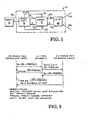
- the filter of the instant invention is preferably included within the encoder 62. With reference to Fig. 3, a state diagram of the filter of the present invention is shown.
- the filter Upon initialization of ENDEC 12, the filter transits to a "through” state. In this state proper symbols are converted and transmitted "through” to the network.
- Reception of the JK symbol pair without a parity error, in the cae of parity-enabled operation, in the "force halt” state causes transition back to the "through” state.
- Reception of the I symbol as the upper "nibble" without a parity error, in the case of parity-enabled operation, in the "force halt” state causes transition back to the "force idle” state.
- the filter remains in the "force halt” state until either four halt symbols are transmitted or reception of an I symbol as the upper "nibble" without a parity error, in the case of parity-enabled operation. Upon occurrence of either event, the filter transitions back to the "force idle” state.
- the filter remains in the "force idle” state until reception of the JK symbol pair without parity error, in the case of parity-enabled operation, or until the encoder 62 is reset.
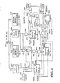
- a set of signal lines being a bus 100, conducts the ten-bit signals generated by the register 60.
- This bus is denoted by the reference numeral 61 in Fig. 2 and also includes the one-bit parity signal).
- a start data (SD) detector 102 receives all ten bit signals conducted on bus 100. SD detector 102 generates a HIGH logic signal on signal line 104 if the JK symbol pair is present on bus 100.
- a Quiet, Halt, Violation, J, K or any undefined symbol (QHVJK) detector 106 receives the upper, or most-significant, 5-bit nibble signals conducted on bus 100, as does an idle detector 108.
- a similar (QHVJK) detector 110 receives the lower, or least-significant, 5-bit nibble signals conducted on bus 100.
- the QHVJK detectors 106 and 110 generate a HIGH logic signal on lines 112, 114 respectively, if one of the symbols Q, H, V, J or K, or undefined symbols, signals are present on the most-significant, least-significant 5-bit signals, respectively, conducted on bus 100.
- the idle detector 108 generates a HIGH logic signal on line 116, if the most significant 5-bit signals conducted on bus 100 represents an idle (I) symbol.
- An OR gate 118 receives the signals conducted on lines 112 and 114 and generates therefrom a signal conducted to a true input of an AND gate 120.
- An AND gate 122 receives the complemented parity error (PE) signal generated by the ENCODER 62 and the PARCON signal generated by node controller 14. The signal generated by AND gate 122 is conducted to the first input of an AND gate 124, and AND 126 and an AND gate 128.
- PE parity error
- a second input of AND gate 124 receives the signal generated on line 104 and generates therefrom a "JK” logic signal; a logic HIGH thereof indicative of the presence of the JK pair of symbols on bus 100 and the absence of a parity error in the unencoded symbols.
- the "JK” signal is also conducted to a first complemented input of AND gate 120.
- a second complemented input of AND gate 120 receives the signal generated on line 116.
- AND gate 120 generates a signal conducted to a second input of AND gate 126 which generates a "QHV" signal therefrom; a HIGH logic signal indicating the presence of either an isolated J or K symbol or a Q, H or V symbol at either the upper or lower nibble of the signals on bus 100, no I symbol in the upper nibble of the signals on bus 100, and the absence of a parity error, in the case of a parity-enabled operation.
- the signal conducted on line 116 is also conducted to a second input of AND gate 128; AND gate 128 generates a HIGH logic signal indicating the presence of an I signal in the upper nibble of the signals on bus 100.
- a set-reset flip-flop 130 receives the byte clock (BCLK) signal at its clock input and a RESET signal at its clear input.
- the "JK" signal generated by AND gate 124 is received at the set input of flip-flop 130.
- the output generated at the (Q) output of flip-flop 130 is conducted to a first input of an AND gate 132; a HIGH logic signal indicating the start of a data packet (SDP).
- the signal generated by AND gate 132 is conducted via signal line 134 to the reset input of flip-flop 130. Accordingly, flip-flop 130 will be reset after the detection of a HIGH QHV signal.
- a second set-reset flip flop 136 receives the signal conducted on line 134 at its set input.
- the BCLK signal is received at the clock input of flip-flop 136 and the RESET signal is received at the clear input of flip-flop 136.
- the signal generated at the (Q) output of flip-flop 136 is conducted to a complement input of an AND gate 138; a HIGH logic signal indicating the presence of one of Q, H, isolated J, isolated K, any undefined symbol or V symbol within a data packet (QHVP).
- the QHVP signal is also conducted to the reset input of flip-flop 136 and to a true input of an AND gate 140.
- the signal conducted on line 134 is conducted to a true input of AND gate 138.
- the "JK" signal generated by AND gate 124 is received at a first complemented input of AND gate 140.
- the SDP signal generated by flip-flop 130 is received at a second complemented input of AND gate 140.
- the signals generated by AND gates 138 and 140 are conducted to the inputs of an OR gate 142.
- the signal generated by OR gate 142 is conducted to a first true input of an AND gate 144.
- a QHV convert (QHVCON) signal 300 is generated by the NODE CONTROLLER 14 indicating enablement of the filter.
- the QHVCON signal is received at a first input of an OR gate 148.
- the output signal generated by OR gate 148 is conducted to the data input of a D-type flip-flop 150.
- the BCLK signal is received at a clock input of flip-flop 150 and the RESET signal is received at a clear input of flip-flop 150.
- the signal generated at the (Q) output of flip-flop 150, a state machine enable (SMSYNC) signal is conducted to a second input of OR gate 148 and a second true input of AND gate 144.
- SMSYNC state machine enable
- a third set-reset flip-flop 152 receives at its set input the signal generated by AND gate 128.
- Flip-flop 152 receives the BCLK signal at its clock input and the RESET signal at its clear input.
- the "JK" signal generated by AND gate 124 is conducted to the reset input of flip-flop 152 and to a complemented input of an AND gate 154.
- the signal generated at the (Q) output of flip-flop 152 is conducted to a true input of AND gate 154.
- the signal generated by AND gate 154 is conducted to a first input of an OR gate 156.
- a second input of OR gate 156 receives the signal generated by AND gate 128.
- An AND gate 158 receives at a first complement input the QHVP signal, at a second complemented input the SDP signal, at a third complemented input the "JK" signal and generates therefrom a signal conducted to a third input of OR gate 156.
- the signal generated by OR gate 156 is conducted to a first input of an AND gate 160.
- a second input of AND gate 160 receives the SMSYNC signal generated by flip-flop 150.
- AND gate 160 generates a FORCE IDLE signal which is conducted to a complemented input of AND gate 144.
- AND gate 144 generates a FORCE HALT signal.
Landscapes
- Engineering & Computer Science (AREA)
- Computer Networks & Wireless Communication (AREA)
- Signal Processing (AREA)
- Multimedia (AREA)
- Computer Hardware Design (AREA)
- Detection And Prevention Of Errors In Transmission (AREA)
- External Artificial Organs (AREA)
- Magnetic Resonance Imaging Apparatus (AREA)
- Liquid Crystal Substances (AREA)
- Data Exchanges In Wide-Area Networks (AREA)
- Networks Using Active Elements (AREA)
- Surgical Instruments (AREA)
- Piezo-Electric Or Mechanical Vibrators, Or Delay Or Filter Circuits (AREA)
- Dc Digital Transmission (AREA)
Priority Applications (1)
| Application Number | Priority Date | Filing Date | Title |
|---|---|---|---|
| AT88110022T ATE103127T1 (de) | 1987-07-15 | 1988-06-23 | Uebertragungsfilter. |
Applications Claiming Priority (2)
| Application Number | Priority Date | Filing Date | Title |
|---|---|---|---|
| US07/073,532 US4835776A (en) | 1987-07-15 | 1987-07-15 | Communication filter |
| US73532 | 1987-07-15 |
Publications (3)
| Publication Number | Publication Date |
|---|---|
| EP0299251A2 true EP0299251A2 (fr) | 1989-01-18 |
| EP0299251A3 EP0299251A3 (en) | 1990-06-13 |
| EP0299251B1 EP0299251B1 (fr) | 1994-03-16 |
Family
ID=22114251
Family Applications (1)
| Application Number | Title | Priority Date | Filing Date |
|---|---|---|---|
| EP88110022A Expired - Lifetime EP0299251B1 (fr) | 1987-07-15 | 1988-06-23 | Filtre de communication |
Country Status (6)
| Country | Link |
|---|---|
| US (1) | US4835776A (fr) |
| EP (1) | EP0299251B1 (fr) |
| JP (1) | JPS6441341A (fr) |
| AT (1) | ATE103127T1 (fr) |
| DE (1) | DE3888412T2 (fr) |
| ES (1) | ES2050129T3 (fr) |
Cited By (2)
| Publication number | Priority date | Publication date | Assignee | Title |
|---|---|---|---|---|
| EP0430052A3 (en) * | 1989-12-01 | 1992-04-15 | National Semiconductor Corporation | Code points for transferring data from a network transmission medium to a station on the network |
| EP0432428A3 (en) * | 1989-11-08 | 1993-09-15 | National Semiconductor Corporation | Byte wide repeat filter |
Families Citing this family (7)
| Publication number | Priority date | Publication date | Assignee | Title |
|---|---|---|---|---|
| US4977559A (en) * | 1988-12-19 | 1990-12-11 | Chrysler Corporation | Improper bit combination detection circuit |
| GB9011700D0 (en) * | 1990-05-25 | 1990-07-18 | Inmos Ltd | Communication interface |
| US5354975A (en) * | 1992-07-01 | 1994-10-11 | Tokimec Inc. | Contactless data processing apparatus |
| US5875210A (en) * | 1993-06-24 | 1999-02-23 | National Semiconductor Corporation | Method and apparatus for repeating data |
| US5566203A (en) * | 1993-06-24 | 1996-10-15 | National Semiconductor Corp. | Intelligent repeater functionality |
| US7385929B1 (en) * | 2001-09-25 | 2008-06-10 | Atheros Communications, Inc. | Method and system for detecting false packets in wireless communications systems |
| US20070098023A1 (en) * | 2005-10-28 | 2007-05-03 | Quantronix Corporation | Fiber laser and methods manufacture and use |
Family Cites Families (4)
| Publication number | Priority date | Publication date | Assignee | Title |
|---|---|---|---|---|
| US4208650A (en) * | 1978-01-30 | 1980-06-17 | Forney Engineering Company | Data transmission system |
| US4703486A (en) * | 1984-12-18 | 1987-10-27 | Advanced Micro Devices, Inc. | Communication data encoder/decoder component system architecture |
| US4692894A (en) * | 1984-12-18 | 1987-09-08 | Advanced Micro Devices, Inc. | Overflow/Underflow detection for elastic buffer |
| US4700358A (en) * | 1985-11-18 | 1987-10-13 | Hayes Microcomputer Products, Inc. | Synchronous/asynchronous modem |
-
1987
- 1987-07-15 US US07/073,532 patent/US4835776A/en not_active Expired - Lifetime
-
1988
- 1988-06-23 AT AT88110022T patent/ATE103127T1/de not_active IP Right Cessation
- 1988-06-23 ES ES88110022T patent/ES2050129T3/es not_active Expired - Lifetime
- 1988-06-23 EP EP88110022A patent/EP0299251B1/fr not_active Expired - Lifetime
- 1988-06-23 DE DE3888412T patent/DE3888412T2/de not_active Expired - Fee Related
- 1988-07-13 JP JP63176207A patent/JPS6441341A/ja active Pending
Cited By (2)
| Publication number | Priority date | Publication date | Assignee | Title |
|---|---|---|---|---|
| EP0432428A3 (en) * | 1989-11-08 | 1993-09-15 | National Semiconductor Corporation | Byte wide repeat filter |
| EP0430052A3 (en) * | 1989-12-01 | 1992-04-15 | National Semiconductor Corporation | Code points for transferring data from a network transmission medium to a station on the network |
Also Published As
| Publication number | Publication date |
|---|---|
| US4835776A (en) | 1989-05-30 |
| DE3888412D1 (de) | 1994-04-21 |
| ATE103127T1 (de) | 1994-04-15 |
| ES2050129T3 (es) | 1994-05-16 |
| JPS6441341A (en) | 1989-02-13 |
| EP0299251B1 (fr) | 1994-03-16 |
| DE3888412T2 (de) | 1994-10-06 |
| EP0299251A3 (en) | 1990-06-13 |
Similar Documents
| Publication | Publication Date | Title |
|---|---|---|
| EP0228214B1 (fr) | Appareil et méthode associée pour convertir des signaux à configuration de données séries transmises, ou appropriées pour une transmission série synchrone à grande vitesse, en signaux de sortie à configuration de données parallèles | |
| US7706433B2 (en) | Physical layer device having an analog SERDES pass through mode | |
| US4972161A (en) | Clock recovery for serial data communications system | |
| US4428046A (en) | Data processing system having a star coupler with contention circuitry | |
| JPH0340543B2 (fr) | ||
| US4903016A (en) | Communication control unit | |
| US5079770A (en) | Apparatus and associated methods for converting serial data pattern signals transmitted or suitable for transmission over a high speed synchronous serial transmission media, to parallel pattern output signals | |
| EP0227378B1 (fr) | Méthode pour recevoir et convertir des signaux d'entrée à configuration de données séries à grande vitesse, en signaux de sortie à configuration de données parallèles | |
| JPH0657010B2 (ja) | データコード間でデータ流れを変換するための変換システム | |
| JP3138170B2 (ja) | マルチステーション・アクセス・ユニット及び複数伝送レート・デジタル・データ通信ネットワーク | |
| JP2953763B2 (ja) | 光トランシーバ | |
| CN100469046C (zh) | 自动协商的系统、方法和设备 | |
| US5442629A (en) | Token ring speed detector | |
| JP3712631B2 (ja) | 伝送方法および伝送システム並びに通信装置 | |
| EP0427066A2 (fr) | Injecteur de motifs | |
| EP0299251B1 (fr) | Filtre de communication | |
| JP2654452B2 (ja) | 非同期で異種の可変幅の並列データパターン入力信号を直列データパターン信号に変換するための装置 | |
| JP2585502B2 (ja) | コ−ド化する方法及びこれを用いた装置 | |
| KR0150211B1 (ko) | 네트워크 전송 매체로부터 네트워크상의 스테이션으로 데이타를 전송하기 위한 코드 포인트 | |
| US5784404A (en) | Intelligent repeater functionality | |
| US5025500A (en) | Apparatus for providing multiple controller interfaces to a standard digital modem and including integral conflict resolution | |
| JP2001527239A (ja) | ディジタルデータを直列伝送するための通信インタフェースおよびデータ伝送方法 | |
| EP0228213B1 (fr) | Système de transmission et de réception de données parallèles asynchrones non homogènes, à largeur variable, sur un moyen de transmission synchrone série à grande vitesse | |
| JP2002101084A (ja) | シリアルデータを同期させるための方法とシステム | |
| JP3277887B2 (ja) | 送受信方法、送受信回路および送受信回路の制御方法 |
Legal Events
| Date | Code | Title | Description |
|---|---|---|---|
| PUAI | Public reference made under article 153(3) epc to a published international application that has entered the european phase |
Free format text: ORIGINAL CODE: 0009012 |
|
| AK | Designated contracting states |
Kind code of ref document: A2 Designated state(s): AT BE CH DE ES FR GB GR IT LI LU NL SE |
|
| PUAL | Search report despatched |
Free format text: ORIGINAL CODE: 0009013 |
|
| AK | Designated contracting states |
Kind code of ref document: A3 Designated state(s): AT BE CH DE ES FR GB GR IT LI LU NL SE |
|
| 17P | Request for examination filed |
Effective date: 19901114 |
|
| 17Q | First examination report despatched |
Effective date: 19930427 |
|
| GRAA | (expected) grant |
Free format text: ORIGINAL CODE: 0009210 |
|
| AK | Designated contracting states |
Kind code of ref document: B1 Designated state(s): AT BE CH DE ES FR GB GR IT LI LU NL SE |
|
| REF | Corresponds to: |
Ref document number: 103127 Country of ref document: AT Date of ref document: 19940415 Kind code of ref document: T |
|
| ITF | It: translation for a ep patent filed | ||
| REF | Corresponds to: |
Ref document number: 3888412 Country of ref document: DE Date of ref document: 19940421 |
|
| REG | Reference to a national code |
Ref country code: ES Ref legal event code: FG2A Ref document number: 2050129 Country of ref document: ES Kind code of ref document: T3 |
|
| REG | Reference to a national code |
Ref country code: GR Ref legal event code: FG4A Free format text: 3011579 |
|
| ET | Fr: translation filed | ||
| EPTA | Lu: last paid annual fee | ||
| PLBE | No opposition filed within time limit |
Free format text: ORIGINAL CODE: 0009261 |
|
| STAA | Information on the status of an ep patent application or granted ep patent |
Free format text: STATUS: NO OPPOSITION FILED WITHIN TIME LIMIT |
|
| EAL | Se: european patent in force in sweden |
Ref document number: 88110022.6 |
|
| 26N | No opposition filed | ||
| PGFP | Annual fee paid to national office [announced via postgrant information from national office to epo] |
Ref country code: NL Payment date: 19980324 Year of fee payment: 11 |
|
| PGFP | Annual fee paid to national office [announced via postgrant information from national office to epo] |
Ref country code: LU Payment date: 19980417 Year of fee payment: 11 |
|
| PGFP | Annual fee paid to national office [announced via postgrant information from national office to epo] |
Ref country code: GR Payment date: 19980430 Year of fee payment: 11 |
|
| PGFP | Annual fee paid to national office [announced via postgrant information from national office to epo] |
Ref country code: AT Payment date: 19980507 Year of fee payment: 11 |
|
| PGFP | Annual fee paid to national office [announced via postgrant information from national office to epo] |
Ref country code: SE Payment date: 19980603 Year of fee payment: 11 Ref country code: FR Payment date: 19980603 Year of fee payment: 11 |
|
| PGFP | Annual fee paid to national office [announced via postgrant information from national office to epo] |
Ref country code: ES Payment date: 19980618 Year of fee payment: 11 |
|
| PGFP | Annual fee paid to national office [announced via postgrant information from national office to epo] |
Ref country code: CH Payment date: 19980708 Year of fee payment: 11 |
|
| PGFP | Annual fee paid to national office [announced via postgrant information from national office to epo] |
Ref country code: BE Payment date: 19980710 Year of fee payment: 11 |
|
| PG25 | Lapsed in a contracting state [announced via postgrant information from national office to epo] |
Ref country code: LU Free format text: LAPSE BECAUSE OF NON-PAYMENT OF DUE FEES Effective date: 19990623 Ref country code: AT Free format text: LAPSE BECAUSE OF NON-PAYMENT OF DUE FEES Effective date: 19990623 |
|
| PG25 | Lapsed in a contracting state [announced via postgrant information from national office to epo] |
Ref country code: ES Free format text: THE PATENT HAS BEEN ANNULLED BY A DECISION OF A NATIONAL AUTHORITY Effective date: 19990624 |
|
| PG25 | Lapsed in a contracting state [announced via postgrant information from national office to epo] |
Ref country code: SE Free format text: THE PATENT HAS BEEN ANNULLED BY A DECISION OF A NATIONAL AUTHORITY Effective date: 19990629 |
|
| PG25 | Lapsed in a contracting state [announced via postgrant information from national office to epo] |
Ref country code: LI Free format text: LAPSE BECAUSE OF NON-PAYMENT OF DUE FEES Effective date: 19990630 Ref country code: GR Free format text: LAPSE BECAUSE OF NON-PAYMENT OF DUE FEES Effective date: 19990630 Ref country code: FR Free format text: THE PATENT HAS BEEN ANNULLED BY A DECISION OF A NATIONAL AUTHORITY Effective date: 19990630 Ref country code: CH Free format text: LAPSE BECAUSE OF NON-PAYMENT OF DUE FEES Effective date: 19990630 Ref country code: BE Free format text: LAPSE BECAUSE OF NON-PAYMENT OF DUE FEES Effective date: 19990630 |
|
| BERE | Be: lapsed |
Owner name: ADVANCED MICRO DEVICES INC. Effective date: 19990630 |
|
| PG25 | Lapsed in a contracting state [announced via postgrant information from national office to epo] |
Ref country code: NL Free format text: LAPSE BECAUSE OF NON-PAYMENT OF DUE FEES Effective date: 20000101 |
|
| REG | Reference to a national code |
Ref country code: CH Ref legal event code: PL |
|
| EUG | Se: european patent has lapsed |
Ref document number: 88110022.6 |
|
| NLV4 | Nl: lapsed or anulled due to non-payment of the annual fee |
Effective date: 20000101 |
|
| REG | Reference to a national code |
Ref country code: FR Ref legal event code: ST |
|
| PGFP | Annual fee paid to national office [announced via postgrant information from national office to epo] |
Ref country code: GB Payment date: 20010502 Year of fee payment: 14 |
|
| PGFP | Annual fee paid to national office [announced via postgrant information from national office to epo] |
Ref country code: DE Payment date: 20010627 Year of fee payment: 14 |
|
| REG | Reference to a national code |
Ref country code: ES Ref legal event code: FD2A Effective date: 20010604 |
|
| REG | Reference to a national code |
Ref country code: GB Ref legal event code: IF02 |
|
| PG25 | Lapsed in a contracting state [announced via postgrant information from national office to epo] |
Ref country code: GB Free format text: LAPSE BECAUSE OF NON-PAYMENT OF DUE FEES Effective date: 20020623 |
|
| PG25 | Lapsed in a contracting state [announced via postgrant information from national office to epo] |
Ref country code: DE Free format text: LAPSE BECAUSE OF NON-PAYMENT OF DUE FEES Effective date: 20030101 |
|
| GBPC | Gb: european patent ceased through non-payment of renewal fee |
Effective date: 20020623 |
|
| PG25 | Lapsed in a contracting state [announced via postgrant information from national office to epo] |
Ref country code: IT Free format text: LAPSE BECAUSE OF NON-PAYMENT OF DUE FEES;WARNING: LAPSES OF ITALIAN PATENTS WITH EFFECTIVE DATE BEFORE 2007 MAY HAVE OCCURRED AT ANY TIME BEFORE 2007. THE CORRECT EFFECTIVE DATE MAY BE DIFFERENT FROM THE ONE RECORDED. Effective date: 20050623 |