EP0299336A2 - Polygon-Spiegel - Google Patents
Polygon-Spiegel Download PDFInfo
- Publication number
- EP0299336A2 EP0299336A2 EP88110733A EP88110733A EP0299336A2 EP 0299336 A2 EP0299336 A2 EP 0299336A2 EP 88110733 A EP88110733 A EP 88110733A EP 88110733 A EP88110733 A EP 88110733A EP 0299336 A2 EP0299336 A2 EP 0299336A2
- Authority
- EP
- European Patent Office
- Prior art keywords
- polygon mirror
- light beam
- center
- inscribed circle
- ellipse
- Prior art date
- Legal status (The legal status is an assumption and is not a legal conclusion. Google has not performed a legal analysis and makes no representation as to the accuracy of the status listed.)
- Granted
Links
Images



Classifications
-
- G—PHYSICS
- G02—OPTICS
- G02B—OPTICAL ELEMENTS, SYSTEMS OR APPARATUS
- G02B26/00—Optical devices or arrangements for the control of light using movable or deformable optical elements
- G02B26/08—Optical devices or arrangements for the control of light using movable or deformable optical elements for controlling the direction of light
- G02B26/10—Scanning systems
-
- G—PHYSICS
- G02—OPTICS
- G02B—OPTICAL ELEMENTS, SYSTEMS OR APPARATUS
- G02B5/00—Optical elements other than lenses
- G02B5/08—Mirrors
- G02B5/09—Multifaceted or polygonal mirrors, e.g. polygonal scanning mirrors; Fresnel mirrors
Definitions
- This invention relates to an improvement of a polygon mirror used in a post-objective type light deflector.
- Optical scanning devices used in optical systems incorporated in laser printers or the like can be divided into two main types: one is the post-objective type, in which light is focused into a beam by a focusing lens and then sent to a light deflector, and the other is the pre-objective type. in which light is first deflected by means of a light deflector and then focused by a focusing lens.
- the focusing lens can therefore be small and simple in construction.
- the beam focusing spot is generally set on a curved surface, an error in the scanning linearity and the curvature of image field will increase.
- the beam is first deflected by the light deflector. before being focused by the focusing lens, so that the beam spot can be easily set on a flat plane and therefore an error in the scanning linearity and the curvature of image field can be easily corrected.
- a wide angle lens such as an fe lens
- the focusing lens in order to obtain a proper deflection angle, making the lens construction complex.
- each of the two types of scanning devices has its advantages as well as disadvantages.
- an error in the curvature of the image field is corrected by use of a polygon mirror having a spherical or cylindrical convex reflection surface with a radius R of curvature, and the error in scanning linearity is corrected by a succeeding electrical correction processing (the clock frequency of the image signal is changed according to variation in the scanning speed).
- the above conventional device has the disadvantage that it is necessary to effect the electrical correction processing in order to correct the error in the scanning linearity.
- An object of the present invention is to provide a polygon mirror, for use with a post objective light deflector, which is capable of suppressing to a minimum, any error in the scanning linearity and the curvature of image field, without effecting the electrical correction processing and enhancing the accuracy of a pattern obtained by a scanning operation.
- Each of the convex reflection surfaces of the above light deflector is defined by part of an imaginary ellipse, the major axis of which is so arranged as to pass through the rotation center of the polygon mirror.
- the ellipse has long and short radii b and c these being the major and minor axes, respectively, and rotation axis O, which passes long radius b and extends in a direction which intersects the major and minor axes (radii b and c) at right angles.
- the radius of an inscribed circle of the polygon mirror is Rm
- the distance from rotation axis O to scanning plane SP is R
- the effective scanning length is Lo.
- rotation angle 0 of the polygon mirror is set at "0", as is also beam position y when the major axis (corresponding to long radius b) crosses scanning plane SP at right angles, and that 9 is set at "8 0 " when beam position y is set at Lo / 2. This being so, the following equations can be obtained in the range of rotation angle e (- ⁇ O ⁇ O) of the polygon mirror:
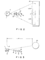
- Fig. 1 shows the construction of a post objective light deflector using polygon mirror 1 according to one embodiment of this invention.
- Figs. 2 and 3 are, respectively, top and side views of Fig. 1.
- laser beam LB emitted from laser diode 10 is irradiated via light collimating objective lens 12, cylindrical lens 14, and spherical lens 16, onto one of six light reflection surfaces of hexagonal polygon mirror 1, from which it is reflected and projected onto scanning plane SP of photoreceptor drum 20, which is set apart from rotation axis O of polygon mirror 1 by distance R.
- Motor 18 is used to rotate polygon mirror 1 so that laser beam LB reflected therefrom can be deflected within a range of ⁇ Lo/2 with respect to the center (focusing position) CT of scanning plane SP of drum 20.
- polygon mirror 1 is illustrated in a sliced-pineapple ring form, but it can be obtained by slicing a hexagonal hollow cylindrical body having convex side surfaces or a football-like body having six side surfaces. Further, each of the six side surfaces has a curvature defined by part of the outer surface of an elliptic cylinder.
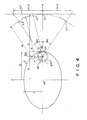
- Fig. 4 shows the geometrical relation between elliptic outer surface 2 of an elliptic cylinder, part of which constitutes one of the reflection surfaces of polygon mirror 1. rotation center 0 of polygon mirror 1, and light beam scanning plane SP. and Fig. 5 is an enlargement of a portion of Fig. 4, showing part of polygon mirror 1.
- short radius c of elliptic outer surface 2 lies on the y axis, and long radius b thereof lies on the x axis.
- Fig. 5 shows an enlargement of a portion of polygon mirror 1 including maximum curvature portion CP.
- polygon mirror 1 has six elliptic mirror surfaces 1a a to 1f, and six edges (i) to (vi) which are in contact with circumscribed circle EXT.
- Mirror surface 1a corresponding to part of elliptic outer surface 2, is symmetrical with respect to the major axis (corresponding to long radius b) which passes through maximum curvature portion CP.
- the curvature of mirror surface 1 a reaches a maximum at maximum curvature portion CP, and gradually decreases at a given rate as a curvature defining point moves from CP to edge (i) or (vi) on mirror surface 1a.
- This feature is obtained by using part of elliptic surface 2 as the mirror surface of polygon mirror 1, and is utilized by the present invention to reduce an error in the curvature of the image field and in the scanning linearity on scanning plane SP, thereby to dispense with the need for an fe lens and electrical error-correction means.
- center 0 of inscribed circuit INT is used as the origin of the x-y plane.
- an axis light beam and differentiated light beam from lens 16 of Fig. 1 are projected to be focused on point So and reflected from the reflection surface to form an image on point S.
- point So is set in position apart from rotation axis 0 by distance t.
- coordinates (xc, yc) of focusing point S are determined as follows, by using x and y axes corresponding to radii b and c of ellipse 2.
- xo and yo can be expressed as a function of ⁇ , as follows:
- ⁇ can be expressed as As can be clearly seen from Fig. 7, differential coefficients dx/d ⁇ and dyid ⁇ can be derived as follows: wherein y can be expressed as
- d ⁇ id ⁇ is the only unknown variable, and can be obtained as follows, based on equations (9), (10), and (11):
- Equations (7) and (8) can be converted into equations (19) and (20) as follows, by using the rotation formula of the following equation (18) and focusing point S (xc, yc) on the fixed coordinate system:
- An optical simulation was effected to detect the condition in which an error in the scanning linearity can be suppressed within ⁇ 2% and the curvature of the image field can be set within 5% of length R of the optical scanning path.
- the rotation angle of 60° of polygon mirror 1 is set to correspond to one scanning cycle, in order that the rotation angle of 40° of polygon mirror 1 can cover the image formation spot area of 220 mm, and an error in the scanning linearity at scanning plane center CT is suppressed to 0.
- Figs. 8A and 8B show the result of simulation in which distance R of focusing point CT from rotation center 0 of polygon mirror 1 was set to 350 mm, radius Rm of the inscribed circle of polygon mirror 1 was set to 22.65625 mm, and long and short radii b and c of ellipse 2 were respectively set to 264.96875 mm and 105.908431 mm.
- Figs. 9A and 9B show the result of simulation in which distance R of focusing point CT from rotation center 0 of polygon mirror 1 was set to 350 mm, radius Rm of the inscribed circle of polygon mirror 1 was set to 24.53125 mm, and long and short radii b and c of ellipse 2 were respectively set to 246.3125 mm and 106.549469 mm.
- Figs. 10A and 10B show the result of simulation in which distance R of focusing point CT from rotation center 0 of polygon mirror 1 was set to 382.65625 mm, radius Rm of the inscribed circle of polygon mirror 1 was set to 25.0 mm, and long and short radii b and c of ellipse 2 were respectively set to 147.671875 mm and 80.2821472 mm.
- Figs. 11 A and 11B show the result of simulation in which distance R of focusing point CT from rotation center 0 of polygon mirror 1 was set to 467.5 mm, radius Rm of the inscribed circle of polygon mirror 1 was set to 25.0 mm, and long and short radii b and c of ellipse 2 were respectively set to 165.46875 mm and 85.6534702 mm.
- Figs. 12a and 12B shown the result of simulation in which distance R of focusing point CT from rotation center 0 of polygon mirror 1 was set to 455.0 mm, radius Rm of the inscribed circle of polygon mirror 1 was set to 25.0 mm, and long and short radii b and c of ellipse 2 were respectively set to 101.265625 mm and 64.8617095 mm.
- Figs. 13A and 13B show the result of simulation in which distance R of focusing point CT from rotation center 0 of polygon mirror 1 was set to 424.375 mm, radius Rm of the inscribed circle of polygon mirror 1 was set to 25.0 mm, and long and short radii b and c of ellipse 2 were respectively set to 147.671875 mm and 80.3066963 mm.
- Figs. 14A and 14B show the result of simulation in which distance R of focusing point CT from rotation center O of polygon mirror 1 was set to 419.375 mm.
- radius Rm of the inscribed circle of polygon mirror 1 was set to 25.0 mm, and long and short radii b and c of ellipse 2 were respectively set to 93.53125 mm and 61.8695557 mm.
- Figs. 15A and 15B show the result of simulation in which distance R of focusing point CT from rotation center 0 of polygon mirror 1 was set to 491.875 mm, radius Rm of the inscribed circle of polygon mirror 1 was set to 25.0 mm, and long and short radii b and c of ellipse 2 were respectively set to 11 S.828125 mm and 71.2061837 mm.
- Figs. 16A and 16B show the result of simulation in which distance R of focusing point CT from rotation center 0 of polygon mirror 1 was set to 443.125 mm, radius Rm of the inscribed circle of polygon mirror 1 was set to 25.0 mm, and long and short radii b and c of ellipse 2 were respectively set to 81.640625 mm and 56.8074427 mm.
- the error in scanning linearity and the curvature of the image field can be suppressed to sufficiently small values by selectively setting distance R of focusing point CT from rotation center 0 of polygon mirror 1, radius Rm of the inscribed circle of polygon mirror 1, and long and short radii b and c of ellipse 2 to suitable values.
- long and short radii b and c of ellipse 2 are respectively set on the x and y axes.
- rotation center 0 can be set to pass through the axis of radius b.
- a post objective light deflector can be provided in which the error in scanning linearity and the curvature of the image field can be suppressed to be sufficiently small without the need to use electrical correction processing, thus enhancing the pattern forming precision.
Landscapes
- Physics & Mathematics (AREA)
- General Physics & Mathematics (AREA)
- Optics & Photonics (AREA)
- Mechanical Optical Scanning Systems (AREA)
- Optical Elements Other Than Lenses (AREA)
Applications Claiming Priority (2)
| Application Number | Priority Date | Filing Date | Title |
|---|---|---|---|
| JP168029/87 | 1987-07-06 | ||
| JP62168029A JP2502314B2 (ja) | 1987-07-06 | 1987-07-06 | ポストオブジェクティブ型光偏向器 |
Publications (3)
| Publication Number | Publication Date |
|---|---|
| EP0299336A2 true EP0299336A2 (de) | 1989-01-18 |
| EP0299336A3 EP0299336A3 (en) | 1989-08-23 |
| EP0299336B1 EP0299336B1 (de) | 1993-06-16 |
Family
ID=15860499
Family Applications (1)
| Application Number | Title | Priority Date | Filing Date |
|---|---|---|---|
| EP88110733A Expired - Lifetime EP0299336B1 (de) | 1987-07-06 | 1988-07-05 | Polygon-Spiegel |
Country Status (5)
| Country | Link |
|---|---|
| US (1) | US4875748A (de) |
| EP (1) | EP0299336B1 (de) |
| JP (1) | JP2502314B2 (de) |
| KR (1) | KR910002009B1 (de) |
| DE (1) | DE3881768T2 (de) |
Cited By (3)
| Publication number | Priority date | Publication date | Assignee | Title |
|---|---|---|---|---|
| EP0420124A3 (en) * | 1989-09-29 | 1992-03-18 | Kabushiki Kaisha Toshiba | Optical unit for use in laser beam printer or the like |
| WO1997021131A3 (en) * | 1995-12-05 | 1997-07-24 | Martin Capey | Scanning system |
| GB2550338A (en) * | 2016-05-12 | 2017-11-22 | Hewlett Packard Development Co Lp | Reflector and additive manufacturing system |
Families Citing this family (15)
| Publication number | Priority date | Publication date | Assignee | Title |
|---|---|---|---|---|
| DE3887610T2 (de) * | 1987-09-22 | 1994-08-25 | Tokyo Electric Co Ltd | Hinter einem Objektiv angeordneter optischer Ablenker. |
| US5204769A (en) * | 1987-09-22 | 1993-04-20 | Tokyo Electric Co., Ltd. | Postobjective optical deflector |
| US5153766A (en) * | 1987-09-22 | 1992-10-06 | Tokyo Electric Co., Ltd. | Postobjective optical scanner |
| JPH01321581A (ja) * | 1988-06-24 | 1989-12-27 | Fujitsu Ltd | バーコード用光学読み取り装置 |
| JP2763148B2 (ja) * | 1989-08-31 | 1998-06-11 | 株式会社東芝 | 走査式光学装置 |
| JP3198103B2 (ja) * | 1989-12-07 | 2001-08-13 | 株式会社東芝 | 光偏向装置の製造方法 |
| JPH03177810A (ja) * | 1989-12-07 | 1991-08-01 | Toshiba Corp | 光偏向装置 |
| JPH03198015A (ja) * | 1989-12-27 | 1991-08-29 | Toshiba Corp | 光学装置 |
| JP3126137B2 (ja) * | 1990-11-01 | 2001-01-22 | 松下電器産業株式会社 | ポストオブジェクティブ型走査光学系及び画像形成装置 |
| US5781325A (en) * | 1994-12-19 | 1998-07-14 | Fuji Xerox Co., Ltd. | Optical scanning apparatus |
| US5650869A (en) * | 1995-05-05 | 1997-07-22 | The United States Of America As Represented By The Administrator Of The National Aeronautics And Space Administration | Point relay scanner utilizing ellipsoidal mirrors |
| US6542304B2 (en) | 1999-05-17 | 2003-04-01 | Toolz, Ltd. | Laser beam device with apertured reflective element |
| US7178947B2 (en) * | 2004-06-04 | 2007-02-20 | Dale Marks | Lighting device with elliptical fresnel mirror |
| KR101720773B1 (ko) * | 2010-08-30 | 2017-03-28 | 에스프린팅솔루션 주식회사 | 회전다면경 및 이를 채용한 광주사장치 |
| US9625709B1 (en) * | 2015-09-29 | 2017-04-18 | Datalogic Usa, Inc. | Reduced windage prismatic polygonal reflector for scanning |
Family Cites Families (6)
| Publication number | Priority date | Publication date | Assignee | Title |
|---|---|---|---|---|
| DE2925734C3 (de) * | 1979-06-26 | 1982-06-24 | Erwin Sick Gmbh Optik-Elektronik, 7808 Waldkirch | Optisches Fehlersuchgerät für Materialbahnen |
| DE3022365A1 (de) * | 1979-11-01 | 1981-05-14 | Barr & Stroud Ltd., Glasgow, Scotland | Optische abtastvorrichtung |
| JPS58105104A (ja) * | 1981-12-17 | 1983-06-22 | Ricoh Co Ltd | 光偏向用回転多面レンズ体 |
| JPS61156020A (ja) * | 1984-12-28 | 1986-07-15 | Ricoh Co Ltd | ポストオブジエクテイブ型光偏向器 |
| JPS61296324A (ja) * | 1985-06-25 | 1986-12-27 | フジトク株式会社 | レ−ザ光走査装置 |
| US4853710A (en) * | 1985-11-29 | 1989-08-01 | Ricoh Co., Ltd. | Imaging by laser beam scanning |
-
1987
- 1987-07-06 JP JP62168029A patent/JP2502314B2/ja not_active Expired - Lifetime
-
1988
- 1988-06-30 KR KR1019880008081A patent/KR910002009B1/ko not_active Expired
- 1988-07-01 US US07/214,605 patent/US4875748A/en not_active Expired - Lifetime
- 1988-07-05 DE DE88110733T patent/DE3881768T2/de not_active Expired - Fee Related
- 1988-07-05 EP EP88110733A patent/EP0299336B1/de not_active Expired - Lifetime
Cited By (4)
| Publication number | Priority date | Publication date | Assignee | Title |
|---|---|---|---|---|
| EP0420124A3 (en) * | 1989-09-29 | 1992-03-18 | Kabushiki Kaisha Toshiba | Optical unit for use in laser beam printer or the like |
| WO1997021131A3 (en) * | 1995-12-05 | 1997-07-24 | Martin Capey | Scanning system |
| GB2550338A (en) * | 2016-05-12 | 2017-11-22 | Hewlett Packard Development Co Lp | Reflector and additive manufacturing system |
| US10611084B2 (en) | 2016-05-12 | 2020-04-07 | Hewlett-Packard Development Company, L.P. | Reflector and additive manufacturing system |
Also Published As
| Publication number | Publication date |
|---|---|
| KR890002688A (ko) | 1989-04-11 |
| JPS6411223A (en) | 1989-01-13 |
| JP2502314B2 (ja) | 1996-05-29 |
| EP0299336B1 (de) | 1993-06-16 |
| US4875748A (en) | 1989-10-24 |
| KR910002009B1 (ko) | 1991-03-30 |
| DE3881768T2 (de) | 1994-01-05 |
| EP0299336A3 (en) | 1989-08-23 |
| DE3881768D1 (de) | 1993-07-22 |
Similar Documents
| Publication | Publication Date | Title |
|---|---|---|
| EP0299336A2 (de) | Polygon-Spiegel | |
| JPH05241094A (ja) | ポストオブジェクティブ型走査光学系と画像形成装置 | |
| EP0433613A1 (de) | Mikroskop-Spektrometer mit Cassegrain-Objektiv | |
| US4984858A (en) | Light beam scanning optical system | |
| US5093745A (en) | Light beam scanning optical system | |
| US4915465A (en) | Laser beam printer using only one side surface of a rotational mirror to scanningly deflect a substantially perpendicular laser beam | |
| US5038156A (en) | Light beam scanning optical system | |
| US5196956A (en) | Beam deflector and laser beam printer using only two inclined reflecting surfaces | |
| EP0309205A1 (de) | Hinter einem Objektiv angeordneter optischer Ablenker | |
| EP0278332B1 (de) | Strahlablenker und damit arbeitender Laserdrucker | |
| JPH08122635A (ja) | 光走査光学系 | |
| JP2530351B2 (ja) | ポストオブジエクテイブ型光走査装置 | |
| JPH1020235A (ja) | 光走査装置 | |
| JP3719301B2 (ja) | 光走査装置 | |
| JPH0786595B2 (ja) | ポストオブジエクテイブ型光走査装置 | |
| JPH0251120A (ja) | 走査光学系 | |
| JP2574400B2 (ja) | 走査光の歪補正装置 | |
| JP2775434B2 (ja) | 走査光学系 | |
| JPH112769A (ja) | 光走査装置 | |
| US5648875A (en) | Optical scannng system having error correction | |
| JPH1020230A (ja) | 光走査装置 | |
| JP2718743B2 (ja) | 光走査装置におけるfθレンズ系 | |
| JPS6145805B2 (de) | ||
| JPS62257119A (ja) | 光走査装置 | |
| JP2982744B2 (ja) | 光走査装置 |
Legal Events
| Date | Code | Title | Description |
|---|---|---|---|
| PUAI | Public reference made under article 153(3) epc to a published international application that has entered the european phase |
Free format text: ORIGINAL CODE: 0009012 |
|
| 17P | Request for examination filed |
Effective date: 19880705 |
|
| AK | Designated contracting states |
Kind code of ref document: A2 Designated state(s): DE FR GB |
|
| PUAL | Search report despatched |
Free format text: ORIGINAL CODE: 0009013 |
|
| AK | Designated contracting states |
Kind code of ref document: A3 Designated state(s): DE FR GB |
|
| 17Q | First examination report despatched |
Effective date: 19911018 |
|
| RBV | Designated contracting states (corrected) |
Designated state(s): DE GB |
|
| GRAA | (expected) grant |
Free format text: ORIGINAL CODE: 0009210 |
|
| AK | Designated contracting states |
Kind code of ref document: B1 Designated state(s): DE GB |
|
| REF | Corresponds to: |
Ref document number: 3881768 Country of ref document: DE Date of ref document: 19930722 |
|
| PLBE | No opposition filed within time limit |
Free format text: ORIGINAL CODE: 0009261 |
|
| STAA | Information on the status of an ep patent application or granted ep patent |
Free format text: STATUS: NO OPPOSITION FILED WITHIN TIME LIMIT |
|
| 26N | No opposition filed | ||
| PGFP | Annual fee paid to national office [announced via postgrant information from national office to epo] |
Ref country code: DE Payment date: 20010625 Year of fee payment: 14 |
|
| PGFP | Annual fee paid to national office [announced via postgrant information from national office to epo] |
Ref country code: GB Payment date: 20010704 Year of fee payment: 14 |
|
| REG | Reference to a national code |
Ref country code: GB Ref legal event code: IF02 |
|
| PG25 | Lapsed in a contracting state [announced via postgrant information from national office to epo] |
Ref country code: GB Free format text: LAPSE BECAUSE OF NON-PAYMENT OF DUE FEES Effective date: 20020705 |
|
| PG25 | Lapsed in a contracting state [announced via postgrant information from national office to epo] |
Ref country code: DE Free format text: LAPSE BECAUSE OF NON-PAYMENT OF DUE FEES Effective date: 20030201 |
|
| GBPC | Gb: european patent ceased through non-payment of renewal fee |
Effective date: 20020705 |