EP0300499A2 - Couche composite supraconductrice - Google Patents
Couche composite supraconductrice Download PDFInfo
- Publication number
- EP0300499A2 EP0300499A2 EP19880111867 EP88111867A EP0300499A2 EP 0300499 A2 EP0300499 A2 EP 0300499A2 EP 19880111867 EP19880111867 EP 19880111867 EP 88111867 A EP88111867 A EP 88111867A EP 0300499 A2 EP0300499 A2 EP 0300499A2
- Authority
- EP
- European Patent Office
- Prior art keywords
- substrate
- film
- superconductor according
- plane
- single crystal
- Prior art date
- Legal status (The legal status is an assumption and is not a legal conclusion. Google has not performed a legal analysis and makes no representation as to the accuracy of the status listed.)
- Granted
Links
Images


Classifications
-
- H—ELECTRICITY
- H10—SEMICONDUCTOR DEVICES; ELECTRIC SOLID-STATE DEVICES NOT OTHERWISE PROVIDED FOR
- H10N—ELECTRIC SOLID-STATE DEVICES NOT OTHERWISE PROVIDED FOR
- H10N60/00—Superconducting devices
- H10N60/01—Manufacture or treatment
- H10N60/0268—Manufacture or treatment of devices comprising copper oxide
- H10N60/0296—Processes for depositing or forming copper oxide superconductor layers
- H10N60/0408—Processes for depositing or forming copper oxide superconductor layers by sputtering
-
- H—ELECTRICITY
- H10—SEMICONDUCTOR DEVICES; ELECTRIC SOLID-STATE DEVICES NOT OTHERWISE PROVIDED FOR
- H10N—ELECTRIC SOLID-STATE DEVICES NOT OTHERWISE PROVIDED FOR
- H10N60/00—Superconducting devices
- H10N60/01—Manufacture or treatment
- H10N60/0268—Manufacture or treatment of devices comprising copper oxide
- H10N60/0296—Processes for depositing or forming copper oxide superconductor layers
- H10N60/0576—Processes for depositing or forming copper oxide superconductor layers characterised by the substrate
- H10N60/0604—Monocrystalline substrates, e.g. epitaxial growth
-
- H—ELECTRICITY
- H10—SEMICONDUCTOR DEVICES; ELECTRIC SOLID-STATE DEVICES NOT OTHERWISE PROVIDED FOR
- H10N—ELECTRIC SOLID-STATE DEVICES NOT OTHERWISE PROVIDED FOR
- H10N60/00—Superconducting devices
- H10N60/01—Manufacture or treatment
- H10N60/0268—Manufacture or treatment of devices comprising copper oxide
- H10N60/0296—Processes for depositing or forming copper oxide superconductor layers
- H10N60/0576—Processes for depositing or forming copper oxide superconductor layers characterised by the substrate
- H10N60/0632—Intermediate layers, e.g. for growth control
-
- Y—GENERAL TAGGING OF NEW TECHNOLOGICAL DEVELOPMENTS; GENERAL TAGGING OF CROSS-SECTIONAL TECHNOLOGIES SPANNING OVER SEVERAL SECTIONS OF THE IPC; TECHNICAL SUBJECTS COVERED BY FORMER USPC CROSS-REFERENCE ART COLLECTIONS [XRACs] AND DIGESTS
- Y10—TECHNICAL SUBJECTS COVERED BY FORMER USPC
- Y10S—TECHNICAL SUBJECTS COVERED BY FORMER USPC CROSS-REFERENCE ART COLLECTIONS [XRACs] AND DIGESTS
- Y10S428/00—Stock material or miscellaneous articles
- Y10S428/901—Printed circuit
-
- Y—GENERAL TAGGING OF NEW TECHNOLOGICAL DEVELOPMENTS; GENERAL TAGGING OF CROSS-SECTIONAL TECHNOLOGIES SPANNING OVER SEVERAL SECTIONS OF THE IPC; TECHNICAL SUBJECTS COVERED BY FORMER USPC CROSS-REFERENCE ART COLLECTIONS [XRACs] AND DIGESTS
- Y10—TECHNICAL SUBJECTS COVERED BY FORMER USPC
- Y10S—TECHNICAL SUBJECTS COVERED BY FORMER USPC CROSS-REFERENCE ART COLLECTIONS [XRACs] AND DIGESTS
- Y10S428/00—Stock material or miscellaneous articles
- Y10S428/922—Static electricity metal bleed-off metallic stock
- Y10S428/9265—Special properties
- Y10S428/93—Electric superconducting
-
- Y—GENERAL TAGGING OF NEW TECHNOLOGICAL DEVELOPMENTS; GENERAL TAGGING OF CROSS-SECTIONAL TECHNOLOGIES SPANNING OVER SEVERAL SECTIONS OF THE IPC; TECHNICAL SUBJECTS COVERED BY FORMER USPC CROSS-REFERENCE ART COLLECTIONS [XRACs] AND DIGESTS
- Y10—TECHNICAL SUBJECTS COVERED BY FORMER USPC
- Y10S—TECHNICAL SUBJECTS COVERED BY FORMER USPC CROSS-REFERENCE ART COLLECTIONS [XRACs] AND DIGESTS
- Y10S505/00—Superconductor technology: apparatus, material, process
- Y10S505/70—High TC, above 30 k, superconducting device, article, or structured stock
- Y10S505/701—Coated or thin film device, i.e. active or passive
- Y10S505/702—Josephson junction present
-
- Y—GENERAL TAGGING OF NEW TECHNOLOGICAL DEVELOPMENTS; GENERAL TAGGING OF CROSS-SECTIONAL TECHNOLOGIES SPANNING OVER SEVERAL SECTIONS OF THE IPC; TECHNICAL SUBJECTS COVERED BY FORMER USPC CROSS-REFERENCE ART COLLECTIONS [XRACs] AND DIGESTS
- Y10—TECHNICAL SUBJECTS COVERED BY FORMER USPC
- Y10S—TECHNICAL SUBJECTS COVERED BY FORMER USPC CROSS-REFERENCE ART COLLECTIONS [XRACs] AND DIGESTS
- Y10S505/00—Superconductor technology: apparatus, material, process
- Y10S505/70—High TC, above 30 k, superconducting device, article, or structured stock
- Y10S505/701—Coated or thin film device, i.e. active or passive
- Y10S505/703—Microelectronic device with superconducting conduction line
-
- Y—GENERAL TAGGING OF NEW TECHNOLOGICAL DEVELOPMENTS; GENERAL TAGGING OF CROSS-SECTIONAL TECHNOLOGIES SPANNING OVER SEVERAL SECTIONS OF THE IPC; TECHNICAL SUBJECTS COVERED BY FORMER USPC CROSS-REFERENCE ART COLLECTIONS [XRACs] AND DIGESTS
- Y10—TECHNICAL SUBJECTS COVERED BY FORMER USPC
- Y10S—TECHNICAL SUBJECTS COVERED BY FORMER USPC CROSS-REFERENCE ART COLLECTIONS [XRACs] AND DIGESTS
- Y10S505/00—Superconductor technology: apparatus, material, process
- Y10S505/70—High TC, above 30 k, superconducting device, article, or structured stock
- Y10S505/704—Wire, fiber, or cable
-
- Y—GENERAL TAGGING OF NEW TECHNOLOGICAL DEVELOPMENTS; GENERAL TAGGING OF CROSS-SECTIONAL TECHNOLOGIES SPANNING OVER SEVERAL SECTIONS OF THE IPC; TECHNICAL SUBJECTS COVERED BY FORMER USPC CROSS-REFERENCE ART COLLECTIONS [XRACs] AND DIGESTS
- Y10—TECHNICAL SUBJECTS COVERED BY FORMER USPC
- Y10T—TECHNICAL SUBJECTS COVERED BY FORMER US CLASSIFICATION
- Y10T428/00—Stock material or miscellaneous articles
- Y10T428/26—Web or sheet containing structurally defined element or component, the element or component having a specified physical dimension
- Y10T428/263—Coating layer not in excess of 5 mils thick or equivalent
- Y10T428/264—Up to 3 mils
- Y10T428/265—1 mil or less
-
- Y—GENERAL TAGGING OF NEW TECHNOLOGICAL DEVELOPMENTS; GENERAL TAGGING OF CROSS-SECTIONAL TECHNOLOGIES SPANNING OVER SEVERAL SECTIONS OF THE IPC; TECHNICAL SUBJECTS COVERED BY FORMER USPC CROSS-REFERENCE ART COLLECTIONS [XRACs] AND DIGESTS
- Y10—TECHNICAL SUBJECTS COVERED BY FORMER USPC
- Y10T—TECHNICAL SUBJECTS COVERED BY FORMER US CLASSIFICATION
- Y10T428/00—Stock material or miscellaneous articles
- Y10T428/31504—Composite [nonstructural laminate]
- Y10T428/31678—Of metal
Definitions
- This invention relates to a superconductor, more particularly to a compound film superconductor.
- A-15 type binary (two-element) compounds such as niobium nitride (NbN) and niobium germanide (Nb3Ge) had been known as high Tc superconductors, but the superconducting transition temperature of these materials was only about 24°K at highest.
- Perovskite type ternary (three-element) compounds have been expected to show higher transition temperatures, and a Ba-La-Cu-O high-Tc-superconductor has been proposed (J. B. Bendorz and K. A. Muller, Zeitschrift für Physik B - Condensed Matter, 64, 189-193, 1986).
- the superconducting mechanism of the Y-Ba-Cu-O type materials is not yet definitely known, but there is a possibility that these materials could have respectively transition temperatures higher than the temperature of liquid nitrogen and it is expected that such compounds would show more useful properties than the conventional binary compounds as high-Tc-superconductors.
- Bi-Si-Ca-Cu-O system H. Maeda et al, Japanese Journal of Applied Physics, 27 , 1988, L209
- T1-Ba-Ca-Cu-O systems Z. Z. Sheng et al, Nature, 332 , 1988, L139
- these oxide superconductive materials can only be produced by a sintering process, so that these superconductive materials are available only in the form of powders or blocks of ceramics.
- the present inventors found that it is possible to form from these materials a high Tc superconductor film retaining well the characteristics of these materials by using film producing techniques such as sputtering etc. and adding a novel concept to the interface structure of the superconductor film. Based on this finding and by further incorporating unique ideas in the film substrate, the present inventors have succeeded in creating a novel superconducting film structure.
- the superconductor according to this invention comprises an oxide film deposited on a metal film formed on a substrate, these oxide containing A, B and Cu and being a ternary (three-element) or quaternary (four-element) compound having an elemental ratio satisfying the following relation: wherein A is at least one element selected from T1, Bi, Sc, Y and lanthanum series elements (atomic number: 57 - 71), and B is at least one elements selected from Ba, Sr, Ca, Be, Mg and Group IIa elements.
- the superconductor of this invention is essentially characterized in that a superconductive film is formed on a metal buffer film.
- the superconductive film is produced from the sputtering target which is made by breaking down its bare material into very fine powder and depositing such powdery target on a substrate, so that the composition of the formed superconductor film is essentially homogeneous as compared with the conventional sintered materials. Also, the superconductive film is homogeneously deposited and it becomes dense and flat on a metal film. Therefore, the present invention can not only realize an extraordinarily high quality superconductor but also increase the potential number of usable substrates, making it possible to obtain a film structure suitable for realizing various type of superconductor devices using superconductive films.
- a ternary or quarternary compound film 13 is deposited, by sputtering for instance, on a metal film 12 formed on the surface of a substrate 11.
- Substrate 11 is designed to hold the superconductive compound film 13.
- This compound film 13 is formed usually at a high temperature on the order of 700°C.
- the superconductive film gave a surface morphology shown in FIG. 3, that is, it became a micro-crystalline plate 20 and was in a state of being directed randomly.
- This film was small in superconducting critical current, high in hygroscopicity because of high vacancy rate, poor in reliability, with a roughened surface and incapable of micro-fabrication such as photoetching.
- a glass coating 14 is first formed on substrate 11 and then a metal film 12 is formed thereon, followed by deposition thereon of a superconductive oxide film at a high temperature of about 700°C as shown in FIG. 4. Quartz glass, high silica glass, borosilica glass, soda-lime glass and oxynitride glass could be effectively used for such glass coating.
- the present inventors also found that certain materials could be advantageously used for the substrate 11 of FIG. 1 for obtaining its best performance.
- a single crystal substrate is effective for forming a highly crystalline ternary or quaternary oxide compound film 13 on the surface of metal film 12 provided on substrate 11.
- the present inventors confirmed that single crystals of magnesium oxide (MgO), sapphire ( ⁇ -A12O3), spinel, strontium titanate (SrTiO3), silicon (Si), silicon compounds, gallium arsenide etc. are effective as substrate material. This was quite a surprising revelation.
- the thickness of metal film 12 is usually in the range of tens to thousands of angstroms ( ⁇ ), so that it is inconceivable from conventional knowledge that the ternary compound film should be influenced by the crystallinity of the substrate therebelow.
- the crystalline structure and chemical composition of the A-B-Cu-o superconductor of this invention are not yet definitely known, but the analyses show that it has an oxygen-defected perovskite structure.
- the present inventors confirmed that when the elemental ratio in the produced film is in the range defined by a superconducting phenomenon is observed in the film through there could be slight differences in transition temperature.
- a sintered A-B-Cu-O ceramic is used as target, but in case the substrate temperature is 700°C, there is seen a tendency that the produced film becomes deficient in Cu as compared with the metal components of the target.
- the present inventors confirmed, however, that this can be overcome by adding about 50% excess amount of Cu in the target. From the above, it was determined that the target composition should be the one defined by which falls in the optimal compositional range of the film. If the target composition is in this range, desired sputtering deposition can be accomplished not only when the target is a plate-like, cylindrical or fiber-like ceramic but also when it is in the form of sintered particles or powders.
- the powder is placed in, for instance, a stainless steel dish.
- a fiber-like substrate it is effective to employ glass fiber, carbon fiber or heat resistant alloy fibers comprising niobium, titanium, tantalum, stainless steel, etc.
- the present inventors confirmed that when fabricating this type of superconductor in a desired form, for example, in a cylindrical form, it is more effective to use as metal-coated substrate so-called sintered chinaware than single crystals, and they also found the most suitable chinaware materials. That is, the present inventors confirmed that alumina, magnesia, zirconia, steatite, forsterite, beryllia, spinel and the like are best suited for use as metal-coated chinaware substrate these materials are excellent in workability and fitness to the substrate 11 of the superconductive film 12. In this case, if suffices if at least the surface of the substate is composed of said chinaware material as in the case of single crystals.
- the present inventors found that there is a preferred direction for crystalline orientation of this type of crystalline substrate. It was discovered that in case of using single crystals of sapphire as substrate, it is possible to integrate the superconductive film of this invention in a silicon device of an SOS (silicon on supphire) structure by heteroepitaxially growing a (100) Si film on the R plane. The present inventors also confirmed that in the case of C plane and a plane sapphire, the integration with an SOS silicone device is possible by heteroepitaxially growing a (111) Si film on the planes.
- SOS silicon on supphire
- the present inventors also confirmed that in the case of spinel single crystal substate, it is possible to integrate the superconductor of this invention with an Si or GaAs device in the same way as in the case of sapphire single crystal substrate by heteroepitaxially growing a (100) Si film or (111) GaAs film on the substrate surface by using the (100) plane spinel.
- a compound film 13 is deposited, by sputtering for instance, on a metal film 12 formed on the surface of an amorphous substrate 15.
- substrate 15 serves for holding the superconductive compound film 13.
- This film 13 is usually deposited at a high temperature of 700°C.
- metal film 12 was interposed between substrate 15 and three-element compound film, the surface assumed a dense state as shown in FIG. 2 and a good superconductive film 13 was obtained.
- amorphous substances such as quartz glass, pyrex, amorphous silicon, etc., are effective for the substrate 15 of FIG. 5.
- a Pt film 12 was deposited on the substrate by DC planer magnetron sputtering as shown in FIG. 1. Deposition was carried out at a sputtering power of 300 V x 30 mA by using Ar gas pressurized to 8 Pa and maintaining the substrate temperature at 250 - 500°C to form a 0.1 ⁇ m thick film. This Pt film was polycrystalline. On this Pt film 12 was deposited a compound film 13 by high frequency planer magnetron sputtering using sintered ErBa2Cu4 ⁇ 5O8 as target. This sputtering deposition of compound film 13 was carried out under Ar gas pressure of 0.5 Pa at a sputtering power of 150 W for a period of one hour by maintaining the substrate temperature at 700°C to form a 0.5 ⁇ m thick film.
- This film showed a room-temperature resistance of 600 ⁇ and a superconducting transition temperature of 88 K.
- a Pt film 12 was deposited on said glass coating 14 by DC planer magnetron sputtering under the following conditions: Ar gas pressure: 8 Pa, sputtering power: 300 V x 30 mA, substrate temperature: 250 - 500°C, film thickness: 0.1 ⁇ m. This Pt film had a polycrystal structure. On this Pt film 12 was deposited a three-element compound superconductive film 13 by high-frequency planer magnetron sputtering using a sintered ErBa2Cu4 ⁇ 5O5 target.
- This deposition was carried out under an Ar gas pressure of 0.5 Pa at a sputtering power of 150 W for a period of one hour by maintaining the substrate temperature at 700°C to form a 0.5 ⁇ m thick film.
- the thus formed superconductive film showed a room-temperature resistance of 600 ⁇ and a superconducting transition temperature of 88 K.
- Described below is another embodiment of the invention in which a superconductive film was formed on an amorphous substrate.
- a Pt film 12 was deposited on a quartz glass substrate 15 by DC planer magnetron sputtering using a Pt plate target. Sputtering was carried out in an 8 Pa argon gas at a sputtering power of 300 V x 30 mA by maintaining the substrate temperature at 250 - 600°C to form a 0.1 ⁇ m thick film. This Pt film was polycrystalline.
- the thus obtained superconductive film showed a room-temperature resistance of 30 ⁇ and a superconducting transition temperature of 90 K.
- the superconductor according to this invention is characterized in that a superconductive compound film is formed on a metal film.
- the superconductive compound film is formed by first breaking down the base superconductive material into a state of very fine particles, which is called "atomic state", and depositing such particulate material on a substrate, so that the composition of the formed superconductor is essentially homogeneous as compared with the conventional sintered products.
- atomic state a state of very fine particles
- the present invention it is possible to form a superconductive film which is dense in its entire structure and also improved in critical current density. Further, the superconductive film of this invention can be integrated with various electronic devices such as Si and GaAs devices and is also appliable as a key material for various types of superconductive devices such as Josephson elements. It is to be noted particularly that there is a possibility that the transition temperature of this type of compound superconductors could be reduced to room temperature. This invention, therefore, can expand the scope of use of superconductors and thus is of high industrial value.
- the present invention can increase the types of substrate usable for superconductors by incorporating a metal film and makes it possible to form on such substrates a high quality superconductive film having a high critical temperature and a high critical current density.
- this invention greatly contributes to the realization of various types of superconductive devices.
Landscapes
- Engineering & Computer Science (AREA)
- Manufacturing & Machinery (AREA)
- Chemical & Material Sciences (AREA)
- Crystallography & Structural Chemistry (AREA)
- Superconductors And Manufacturing Methods Therefor (AREA)
- Superconductor Devices And Manufacturing Methods Thereof (AREA)
Applications Claiming Priority (8)
| Application Number | Priority Date | Filing Date | Title |
|---|---|---|---|
| JP62186153A JP2802063B2 (ja) | 1987-07-24 | 1987-07-24 | 超電導体 |
| JP186153/87 | 1987-07-24 | ||
| JP186154/87 | 1987-07-24 | ||
| JP62186154A JPS6430112A (en) | 1987-07-24 | 1987-07-24 | Superconductor |
| JP62189279A JPS6433816A (en) | 1987-07-29 | 1987-07-29 | Superconductor |
| JP189279/87 | 1987-07-29 | ||
| JP62189280A JPS6433817A (en) | 1987-07-29 | 1987-07-29 | Superconductor |
| JP189280/87 | 1987-07-29 |
Publications (4)
| Publication Number | Publication Date |
|---|---|
| EP0300499A2 true EP0300499A2 (fr) | 1989-01-25 |
| EP0300499A3 EP0300499A3 (en) | 1990-12-19 |
| EP0300499B1 EP0300499B1 (fr) | 1994-09-28 |
| EP0300499B2 EP0300499B2 (fr) | 1998-08-19 |
Family
ID=27475261
Family Applications (1)
| Application Number | Title | Priority Date | Filing Date |
|---|---|---|---|
| EP19880111867 Expired - Lifetime EP0300499B2 (fr) | 1987-07-24 | 1988-07-22 | Couche composite supraconductrice |
Country Status (3)
| Country | Link |
|---|---|
| US (3) | US5661112A (fr) |
| EP (1) | EP0300499B2 (fr) |
| DE (1) | DE3851668T3 (fr) |
Cited By (11)
| Publication number | Priority date | Publication date | Assignee | Title |
|---|---|---|---|---|
| EP0301525A3 (en) * | 1987-07-29 | 1990-06-20 | Matsushita Electric Industrial Co., Ltd. | Superconductor structure |
| EP0346494A4 (en) * | 1987-12-25 | 1990-10-10 | Mitsubishi Metal Corporation | Superconducting wire structure |
| EP0303083A3 (fr) * | 1987-08-13 | 1990-12-19 | EASTMAN KODAK COMPANY (a New Jersey corporation) | Couche barrière contenant des éléments conducteurs |
| US5202305A (en) * | 1989-04-17 | 1993-04-13 | Ngk Insulators, Ltd. | Superconducting structure for magnetic shielding |
| US5661112A (en) * | 1987-07-24 | 1997-08-26 | Hatta; Shinichiro | Superconductor |
| EP0828333A3 (fr) * | 1996-08-26 | 1998-04-22 | Abb Research Ltd. | Procédé pour la fabrication d'un limiteur de courant à supraconducteur à haute température et limiteur de courant |
| WO1999023707A1 (fr) * | 1997-11-04 | 1999-05-14 | Siemens Aktiengesellschaft | Structure comportant un materiau supraconducteur a haute temperature de transition, et procede de production de cette structure |
| US6440904B1 (en) | 1997-10-24 | 2002-08-27 | Abb Research Ltd | High-temperature superconductor arrangement |
| WO2002054495A3 (fr) * | 2001-01-05 | 2002-11-21 | Motorola Inc | Nitrures d'oxyde metallique presentant un courant de fuite limite |
| RU2304827C1 (ru) * | 2006-04-03 | 2007-08-20 | Государственное образовательное учреждение высшего профессионального образования Марийский государственный технический университет | Способ формирования высокотемпературного сверхпроводникового покрытия |
| FR2967820A1 (fr) * | 2010-11-19 | 2012-05-25 | Nexans | Conducteur de transport d'energie electrique |
Families Citing this family (42)
| Publication number | Priority date | Publication date | Assignee | Title |
|---|---|---|---|---|
| US5741377A (en) * | 1995-04-10 | 1998-04-21 | Martin Marietta Energy Systems, Inc. | Structures having enhanced biaxial texture and method of fabricating same |
| US6387525B1 (en) * | 1997-04-14 | 2002-05-14 | Florida State University | Self insulating substrate tape |
| US6372356B1 (en) | 1998-06-04 | 2002-04-16 | Xerox Corporation | Compliant substrates for growing lattice mismatched films |
| KR100309675B1 (ko) * | 1998-11-23 | 2001-12-17 | 오길록 | 고온초전도계단형모서리조셉슨접합제작방법 |
| US6248459B1 (en) * | 1999-03-22 | 2001-06-19 | Motorola, Inc. | Semiconductor structure having a crystalline alkaline earth metal oxide interface with silicon |
| US6693033B2 (en) | 2000-02-10 | 2004-02-17 | Motorola, Inc. | Method of removing an amorphous oxide from a monocrystalline surface |
| US6392257B1 (en) | 2000-02-10 | 2002-05-21 | Motorola Inc. | Semiconductor structure, semiconductor device, communicating device, integrated circuit, and process for fabricating the same |
| KR20030011083A (ko) | 2000-05-31 | 2003-02-06 | 모토로라 인코포레이티드 | 반도체 디바이스 및 이를 제조하기 위한 방법 |
| US6590236B1 (en) | 2000-07-24 | 2003-07-08 | Motorola, Inc. | Semiconductor structure for use with high-frequency signals |
| AU2001277001A1 (en) | 2000-07-24 | 2002-02-05 | Motorola, Inc. | Heterojunction tunneling diodes and process for fabricating same |
| US6555946B1 (en) | 2000-07-24 | 2003-04-29 | Motorola, Inc. | Acoustic wave device and process for forming the same |
| US6638838B1 (en) | 2000-10-02 | 2003-10-28 | Motorola, Inc. | Semiconductor structure including a partially annealed layer and method of forming the same |
| US20020096683A1 (en) | 2001-01-19 | 2002-07-25 | Motorola, Inc. | Structure and method for fabricating GaN devices utilizing the formation of a compliant substrate |
| US6673646B2 (en) | 2001-02-28 | 2004-01-06 | Motorola, Inc. | Growth of compound semiconductor structures on patterned oxide films and process for fabricating same |
| WO2002082551A1 (fr) | 2001-04-02 | 2002-10-17 | Motorola, Inc. | Structure de semi-conducteur a courant de fuite attenue |
| US6709989B2 (en) | 2001-06-21 | 2004-03-23 | Motorola, Inc. | Method for fabricating a semiconductor structure including a metal oxide interface with silicon |
| US6992321B2 (en) | 2001-07-13 | 2006-01-31 | Motorola, Inc. | Structure and method for fabricating semiconductor structures and devices utilizing piezoelectric materials |
| JP3506428B2 (ja) * | 2001-07-13 | 2004-03-15 | 株式会社東芝 | 高周波部材 |
| US6646293B2 (en) | 2001-07-18 | 2003-11-11 | Motorola, Inc. | Structure for fabricating high electron mobility transistors utilizing the formation of complaint substrates |
| US6693298B2 (en) | 2001-07-20 | 2004-02-17 | Motorola, Inc. | Structure and method for fabricating epitaxial semiconductor on insulator (SOI) structures and devices utilizing the formation of a compliant substrate for materials used to form same |
| US7019332B2 (en) | 2001-07-20 | 2006-03-28 | Freescale Semiconductor, Inc. | Fabrication of a wavelength locker within a semiconductor structure |
| US6855992B2 (en) | 2001-07-24 | 2005-02-15 | Motorola Inc. | Structure and method for fabricating configurable transistor devices utilizing the formation of a compliant substrate for materials used to form the same |
| US6667196B2 (en) | 2001-07-25 | 2003-12-23 | Motorola, Inc. | Method for real-time monitoring and controlling perovskite oxide film growth and semiconductor structure formed using the method |
| US6589856B2 (en) | 2001-08-06 | 2003-07-08 | Motorola, Inc. | Method and apparatus for controlling anti-phase domains in semiconductor structures and devices |
| US6639249B2 (en) | 2001-08-06 | 2003-10-28 | Motorola, Inc. | Structure and method for fabrication for a solid-state lighting device |
| US20030034491A1 (en) | 2001-08-14 | 2003-02-20 | Motorola, Inc. | Structure and method for fabricating semiconductor structures and devices for detecting an object |
| US6673667B2 (en) | 2001-08-15 | 2004-01-06 | Motorola, Inc. | Method for manufacturing a substantially integral monolithic apparatus including a plurality of semiconductor materials |
| US20030071327A1 (en) | 2001-10-17 | 2003-04-17 | Motorola, Inc. | Method and apparatus utilizing monocrystalline insulator |
| US6916717B2 (en) | 2002-05-03 | 2005-07-12 | Motorola, Inc. | Method for growing a monocrystalline oxide layer and for fabricating a semiconductor device on a monocrystalline substrate |
| US7169619B2 (en) | 2002-11-19 | 2007-01-30 | Freescale Semiconductor, Inc. | Method for fabricating semiconductor structures on vicinal substrates using a low temperature, low pressure, alkaline earth metal-rich process |
| US6885065B2 (en) | 2002-11-20 | 2005-04-26 | Freescale Semiconductor, Inc. | Ferromagnetic semiconductor structure and method for forming the same |
| US7020374B2 (en) | 2003-02-03 | 2006-03-28 | Freescale Semiconductor, Inc. | Optical waveguide structure and method for fabricating the same |
| US6965128B2 (en) | 2003-02-03 | 2005-11-15 | Freescale Semiconductor, Inc. | Structure and method for fabricating semiconductor microresonator devices |
| JP2007200870A (ja) * | 2006-01-26 | 2007-08-09 | Ls Cable Ltd | 超伝導ケーブル用基板の製造方法 |
| DE102006036798B4 (de) * | 2006-08-07 | 2013-08-29 | Infineon Technologies Ag | Elektronisches Bauteil und Verfahren zum Herstellen |
| US7615385B2 (en) | 2006-09-20 | 2009-11-10 | Hypres, Inc | Double-masking technique for increasing fabrication yield in superconducting electronics |
| WO2011041765A1 (fr) * | 2009-10-02 | 2011-04-07 | Ambature L.L.C. | Matériaux supraconducteurs à haute température et procédés de modification et de production de ceux ci |
| CN102113141B (zh) * | 2009-10-22 | 2013-02-13 | 松下电器产业株式会社 | 热电转换材料和热电转换元件 |
| US9240317B2 (en) | 2013-03-28 | 2016-01-19 | Umm Al-Qura University | High temperature GaN based super semiconductor and fabrication process |
| WO2017040598A1 (fr) * | 2015-08-31 | 2017-03-09 | Massachusetts Institute Of Technology | Systèmes et procédés pour milieu supraconducteur hybride |
| US10847706B2 (en) | 2015-09-01 | 2020-11-24 | Massachusetts Institute Of Technology | Systems and methods for hybrid superconducting medium comprising first and second layers with different superconductor to induce a proximity effect between thereof |
| US11201273B2 (en) * | 2019-09-13 | 2021-12-14 | Microsoft Technology Licensing, Llc | Semiconductor-superconductor heterostructure |
Family Cites Families (10)
| Publication number | Priority date | Publication date | Assignee | Title |
|---|---|---|---|---|
| KR0132061B1 (ko) * | 1987-03-14 | 1998-04-24 | 나까하라 쯔네오 | 초전도 박막의 제작 방법 |
| DE3887910T2 (de) * | 1987-03-20 | 1994-08-04 | Fujikura Ltd., Tokio/Tokyo | Verfahren zur Herstellung eines Drahtes aus supraleitendem Oxid und damit hergestellter Draht. |
| US4826808A (en) * | 1987-03-27 | 1989-05-02 | Massachusetts Institute Of Technology | Preparation of superconducting oxides and oxide-metal composites |
| US4952554A (en) * | 1987-04-01 | 1990-08-28 | At&T Bell Laboratories | Apparatus and systems comprising a clad superconductive oxide body, and method for producing such body |
| EP0290331B1 (fr) * | 1987-05-01 | 1997-03-05 | Sumitomo Electric Industries Limited | Composite supraconducteur |
| US4880770A (en) * | 1987-05-04 | 1989-11-14 | Eastman Kodak Company | Metalorganic deposition process for preparing superconducting oxide films |
| US5017551A (en) * | 1987-05-04 | 1991-05-21 | Eastman Kodak Company | Barrier layer containing conductive articles |
| JPH0280303A (ja) * | 1987-06-04 | 1990-03-20 | Tonen Corp | 超伝導体薄膜の形成方法及びその為の装置 |
| DE3851668T3 (de) * | 1987-07-24 | 1999-03-04 | Matsushita Electric Industrial Co., Ltd., Kadoma, Osaka | Zusammengesetzte supraleitende Schicht. |
| US4975413A (en) * | 1987-08-12 | 1990-12-04 | Amoco Corporation | Superconductor-coated carbon fiber composites |
-
1988
- 1988-07-22 DE DE3851668T patent/DE3851668T3/de not_active Expired - Fee Related
- 1988-07-22 US US07/223,016 patent/US5661112A/en not_active Ceased
- 1988-07-22 EP EP19880111867 patent/EP0300499B2/fr not_active Expired - Lifetime
-
1998
- 1998-03-06 US US09/035,783 patent/USRE36814E/en not_active Expired - Fee Related
- 1998-11-09 US US09/188,232 patent/US5998337A/en not_active Expired - Fee Related
Non-Patent Citations (3)
| Title |
|---|
| APPLIED PHYSICS LETTERS vol. 51, no. 25, 21 December 1987, pages 2155-2157, New York, US; C.L. CHIEN et al.: "Effect of noble metal buffer layers on superconducting YBa2Cu307 thin films" * |
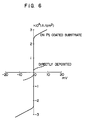
| APPLIED PHYSICS LETTERS vol. 53, no. 2, 11 July 1988, pages 148-150, New York, US; S.Hatta et al.: "Pt-Coated Substrate Effect on Oxide Superconductive Films in Low-Temperature Processing" * |
| FERROELECTRICS, vol. 63, nos. 1-4, 1985, pages 227-234, New York, US; T. Shiosaki et al.: "Properties of Sputter-Deposited PbTi03, Pb(Zr,Ti)03, Pb2KNb5015 Films" * |
Cited By (15)
| Publication number | Priority date | Publication date | Assignee | Title |
|---|---|---|---|---|
| US5661112A (en) * | 1987-07-24 | 1997-08-26 | Hatta; Shinichiro | Superconductor |
| USRE36814E (en) * | 1987-07-24 | 2000-08-08 | Matsushita Electric Industrial Co., Ltd. | Superconductor |
| US5998337A (en) * | 1987-07-24 | 1999-12-07 | Matsushita Electric Industrial Co., Ltd. | Superconductor |
| US4980339A (en) * | 1987-07-29 | 1990-12-25 | Matsushita Electric Industrial Co., Ltd. | Superconductor structure |
| EP0301525A3 (en) * | 1987-07-29 | 1990-06-20 | Matsushita Electric Industrial Co., Ltd. | Superconductor structure |
| EP0303083A3 (fr) * | 1987-08-13 | 1990-12-19 | EASTMAN KODAK COMPANY (a New Jersey corporation) | Couche barrière contenant des éléments conducteurs |
| EP0346494A4 (en) * | 1987-12-25 | 1990-10-10 | Mitsubishi Metal Corporation | Superconducting wire structure |
| US5202305A (en) * | 1989-04-17 | 1993-04-13 | Ngk Insulators, Ltd. | Superconducting structure for magnetic shielding |
| EP0828333A3 (fr) * | 1996-08-26 | 1998-04-22 | Abb Research Ltd. | Procédé pour la fabrication d'un limiteur de courant à supraconducteur à haute température et limiteur de courant |
| US6440904B1 (en) | 1997-10-24 | 2002-08-27 | Abb Research Ltd | High-temperature superconductor arrangement |
| WO1999023707A1 (fr) * | 1997-11-04 | 1999-05-14 | Siemens Aktiengesellschaft | Structure comportant un materiau supraconducteur a haute temperature de transition, et procede de production de cette structure |
| US6391828B1 (en) | 1997-11-04 | 2002-05-21 | Siemens Aktiengesellschaft | Construction with high Tc superconductor material and process for producing the construction |
| WO2002054495A3 (fr) * | 2001-01-05 | 2002-11-21 | Motorola Inc | Nitrures d'oxyde metallique presentant un courant de fuite limite |
| RU2304827C1 (ru) * | 2006-04-03 | 2007-08-20 | Государственное образовательное учреждение высшего профессионального образования Марийский государственный технический университет | Способ формирования высокотемпературного сверхпроводникового покрытия |
| FR2967820A1 (fr) * | 2010-11-19 | 2012-05-25 | Nexans | Conducteur de transport d'energie electrique |
Also Published As
| Publication number | Publication date |
|---|---|
| DE3851668T3 (de) | 1999-03-04 |
| DE3851668D1 (de) | 1994-11-03 |
| EP0300499B1 (fr) | 1994-09-28 |
| EP0300499B2 (fr) | 1998-08-19 |
| US5998337A (en) | 1999-12-07 |
| US5661112A (en) | 1997-08-26 |
| EP0300499A3 (en) | 1990-12-19 |
| DE3851668T2 (de) | 1995-05-04 |
| USRE36814E (en) | 2000-08-08 |
Similar Documents
| Publication | Publication Date | Title |
|---|---|---|
| EP0300499B2 (fr) | Couche composite supraconductrice | |
| EP0301525B1 (fr) | Structure supraconductrice | |
| US4994435A (en) | Laminated layers of a substrate, noble metal, and interlayer underneath an oxide superconductor | |
| EP0430737B1 (fr) | Un film mince supraconducteur | |
| CA2020302C (fr) | Substrat enduit d'une pellicule supraconductrice | |
| US5162294A (en) | Buffer layer for copper oxide based superconductor growth on sapphire | |
| EP0446789B1 (fr) | Procédé pour la fabrication d'une couche d'oxyde supraconductrice | |
| US4983575A (en) | Superconducting thin films made of stacked composite oxide layers | |
| EP0465326B1 (fr) | Film mince supraconducteur d'oxyde composé et procédé pour sa préparation | |
| EP0341148B1 (fr) | Substrat semiconducteur ayant une couche mince supraconductrice | |
| Chen et al. | Growth of epitaxial YbBa2Cu3O7 superconductor by liquid‐gas‐solidification processing | |
| EP0304078B1 (fr) | Structure de couche composite supraconductrice | |
| US5416062A (en) | Thin film superconductor with an interlayer on a silicon substrate | |
| EP0357500B1 (fr) | Procédé pour préparer un film mince supraconducteur de type bismuth | |
| EP1443131B1 (fr) | Oxyde supraconducteur haute temperature et son procede de production | |
| JPH07102969B2 (ja) | 超電導体 | |
| JP2506798B2 (ja) | 超電導体 | |
| JPS63224113A (ja) | 超電導体 | |
| JP2590142B2 (ja) | 超伝導体 | |
| EP0519769B1 (fr) | Procédé pour la préparation d'un film mince supraconducteur en oxyde composé | |
| JPH07106896B2 (ja) | 超電導体 | |
| JP2802063B2 (ja) | 超電導体 | |
| JP2899285B2 (ja) | 超電導体 | |
| EP0333513B1 (fr) | Oxyde supraconducteur | |
| JPH07106895B2 (ja) | 超電導体構造物 |
Legal Events
| Date | Code | Title | Description |
|---|---|---|---|
| PUAI | Public reference made under article 153(3) epc to a published international application that has entered the european phase |
Free format text: ORIGINAL CODE: 0009012 |
|
| AK | Designated contracting states |
Kind code of ref document: A2 Designated state(s): DE FR GB |
|
| PUAL | Search report despatched |
Free format text: ORIGINAL CODE: 0009013 |
|
| AK | Designated contracting states |
Kind code of ref document: A3 Designated state(s): DE FR GB |
|
| 17P | Request for examination filed |
Effective date: 19901228 |
|
| 17Q | First examination report despatched |
Effective date: 19930429 |
|
| GRAA | (expected) grant |
Free format text: ORIGINAL CODE: 0009210 |
|
| AK | Designated contracting states |
Kind code of ref document: B1 Designated state(s): DE FR GB |
|
| REF | Corresponds to: |
Ref document number: 3851668 Country of ref document: DE Date of ref document: 19941103 |
|
| ET | Fr: translation filed | ||
| PLBI | Opposition filed |
Free format text: ORIGINAL CODE: 0009260 |
|
| 26 | Opposition filed |
Opponent name: SIEMENS AG Effective date: 19950626 |
|
| PLBF | Reply of patent proprietor to notice(s) of opposition |
Free format text: ORIGINAL CODE: EPIDOS OBSO |
|
| PLBF | Reply of patent proprietor to notice(s) of opposition |
Free format text: ORIGINAL CODE: EPIDOS OBSO |
|
| PLAW | Interlocutory decision in opposition |
Free format text: ORIGINAL CODE: EPIDOS IDOP |
|
| PLAW | Interlocutory decision in opposition |
Free format text: ORIGINAL CODE: EPIDOS IDOP |
|
| PUAH | Patent maintained in amended form |
Free format text: ORIGINAL CODE: 0009272 |
|
| STAA | Information on the status of an ep patent application or granted ep patent |
Free format text: STATUS: PATENT MAINTAINED AS AMENDED |
|
| 27A | Patent maintained in amended form |
Effective date: 19980819 |
|
| AK | Designated contracting states |
Kind code of ref document: B2 Designated state(s): DE FR GB |
|
| ET3 | Fr: translation filed ** decision concerning opposition | ||
| REG | Reference to a national code |
Ref country code: GB Ref legal event code: IF02 |
|
| PGFP | Annual fee paid to national office [announced via postgrant information from national office to epo] |
Ref country code: FR Payment date: 20050708 Year of fee payment: 18 |
|
| PGFP | Annual fee paid to national office [announced via postgrant information from national office to epo] |
Ref country code: DE Payment date: 20050714 Year of fee payment: 18 |
|
| PGFP | Annual fee paid to national office [announced via postgrant information from national office to epo] |
Ref country code: GB Payment date: 20050720 Year of fee payment: 18 |
|
| PG25 | Lapsed in a contracting state [announced via postgrant information from national office to epo] |
Ref country code: GB Free format text: LAPSE BECAUSE OF NON-PAYMENT OF DUE FEES Effective date: 20060722 |
|
| PG25 | Lapsed in a contracting state [announced via postgrant information from national office to epo] |
Ref country code: DE Free format text: LAPSE BECAUSE OF NON-PAYMENT OF DUE FEES Effective date: 20070201 |
|
| GBPC | Gb: european patent ceased through non-payment of renewal fee |
Effective date: 20060722 |
|
| REG | Reference to a national code |
Ref country code: FR Ref legal event code: ST Effective date: 20070330 |
|
| PG25 | Lapsed in a contracting state [announced via postgrant information from national office to epo] |
Ref country code: FR Free format text: LAPSE BECAUSE OF NON-PAYMENT OF DUE FEES Effective date: 20060731 |