EP0301335B1 - Procédé d'attaque sèche - Google Patents
Procédé d'attaque sèche Download PDFInfo
- Publication number
- EP0301335B1 EP0301335B1 EP88111438A EP88111438A EP0301335B1 EP 0301335 B1 EP0301335 B1 EP 0301335B1 EP 88111438 A EP88111438 A EP 88111438A EP 88111438 A EP88111438 A EP 88111438A EP 0301335 B1 EP0301335 B1 EP 0301335B1
- Authority
- EP
- European Patent Office
- Prior art keywords
- etching
- temperature
- article
- etched
- film
- Prior art date
- Legal status (The legal status is an assumption and is not a legal conclusion. Google has not performed a legal analysis and makes no representation as to the accuracy of the status listed.)
- Expired - Lifetime
Links
Images


Classifications
-
- H—ELECTRICITY
- H10—SEMICONDUCTOR DEVICES; ELECTRIC SOLID-STATE DEVICES NOT OTHERWISE PROVIDED FOR
- H10P—GENERIC PROCESSES OR APPARATUS FOR THE MANUFACTURE OR TREATMENT OF DEVICES COVERED BY CLASS H10
- H10P50/00—Etching of wafers, substrates or parts of devices
- H10P50/20—Dry etching; Plasma etching; Reactive-ion etching
- H10P50/26—Dry etching; Plasma etching; Reactive-ion etching of conductive or resistive materials
- H10P50/264—Dry etching; Plasma etching; Reactive-ion etching of conductive or resistive materials by chemical means
- H10P50/266—Dry etching; Plasma etching; Reactive-ion etching of conductive or resistive materials by chemical means by vapour etching only
- H10P50/267—Dry etching; Plasma etching; Reactive-ion etching of conductive or resistive materials by chemical means by vapour etching only using plasmas
- H10P50/268—Dry etching; Plasma etching; Reactive-ion etching of conductive or resistive materials by chemical means by vapour etching only using plasmas of silicon-containing layers
-
- H—ELECTRICITY
- H10—SEMICONDUCTOR DEVICES; ELECTRIC SOLID-STATE DEVICES NOT OTHERWISE PROVIDED FOR
- H10P—GENERIC PROCESSES OR APPARATUS FOR THE MANUFACTURE OR TREATMENT OF DEVICES COVERED BY CLASS H10
- H10P50/00—Etching of wafers, substrates or parts of devices
- H10P50/20—Dry etching; Plasma etching; Reactive-ion etching
- H10P50/24—Dry etching; Plasma etching; Reactive-ion etching of semiconductor materials
- H10P50/242—Dry etching; Plasma etching; Reactive-ion etching of semiconductor materials of Group IV materials
-
- H—ELECTRICITY
- H10—SEMICONDUCTOR DEVICES; ELECTRIC SOLID-STATE DEVICES NOT OTHERWISE PROVIDED FOR
- H10P—GENERIC PROCESSES OR APPARATUS FOR THE MANUFACTURE OR TREATMENT OF DEVICES COVERED BY CLASS H10
- H10P50/00—Etching of wafers, substrates or parts of devices
- H10P50/20—Dry etching; Plasma etching; Reactive-ion etching
- H10P50/26—Dry etching; Plasma etching; Reactive-ion etching of conductive or resistive materials
- H10P50/264—Dry etching; Plasma etching; Reactive-ion etching of conductive or resistive materials by chemical means
- H10P50/266—Dry etching; Plasma etching; Reactive-ion etching of conductive or resistive materials by chemical means by vapour etching only
- H10P50/267—Dry etching; Plasma etching; Reactive-ion etching of conductive or resistive materials by chemical means by vapour etching only using plasmas
-
- H—ELECTRICITY
- H10—SEMICONDUCTOR DEVICES; ELECTRIC SOLID-STATE DEVICES NOT OTHERWISE PROVIDED FOR
- H10P—GENERIC PROCESSES OR APPARATUS FOR THE MANUFACTURE OR TREATMENT OF DEVICES COVERED BY CLASS H10
- H10P50/00—Etching of wafers, substrates or parts of devices
- H10P50/20—Dry etching; Plasma etching; Reactive-ion etching
- H10P50/28—Dry etching; Plasma etching; Reactive-ion etching of insulating materials
- H10P50/282—Dry etching; Plasma etching; Reactive-ion etching of insulating materials of inorganic materials
- H10P50/283—Dry etching; Plasma etching; Reactive-ion etching of insulating materials of inorganic materials by chemical means
Definitions
- the present invention relates to a method of dry etching and particularly to a method of low-temperature dry etching suitable for formation of various patterns having a tapered sidewall.
- a conventional method of taper dry etching proposed in, for example, Proceeding of Dry Process Symposium, (IEE of JAPAN, Tokyo) P48 (1986) comprises etching an article to be etched by introducing a mixture composed of an etching gas and a depositing type gas into a reaction chamber.
- this method has a problem that the incorporation of a depositing type gas brings about lowering in both the etching rate and the selection ratio. Further, since the depositing type gas is deposited on a semiconductor substrate to be etched, the deposition brings about the contamination of the surface of the substrate. This in turn causes a lowering in the yield of the product.
- EP-A-0 258 698 which is an Article 54(3) EPC Document, discloses a dry-etching method in which vertical sidewalls are formed by maintaining the article surface at a predetermined, low temperature.
- Any desired tapering sidewall profile including a substantially vertical surface portion is obtained by correspondingly varying the temperature of the article during the etching process.
- depositing type gas used herein is intended to mean a gas containing C or Si, such as CCl4, which causes the deposition of a polymer or the like on the substrate during etching
- non-depositing type gas used herein is intended to mean a gas free from C and Si which causes little or no deposition of a polymer or the like on the substrate during etching.
- Figs. 1a and 1b are each an example of taper etching of a 2 ⁇ m-thick film 2 comprising aluminum or an alloy mainly composed of aluminum, such as aluminum-silicon, deposited on a silicon substrate 1.
- a photoresist film 3 was used as an etching mask of the aluminum or aluminum-base alloy film 2.
- Reactive ion etching was conducted by making use of an etching gas comprising a Cl2 gas under conditions of a pressure chamber pressure of 13 Pa and an input power of 400 W.
- the substrate to be etched was placed on a cooling table of a well-known plane-parallel plate dry etching apparatus, and a temperature controlling (+200°C - -150°C) mechanism was provided so that the temperature of the substrate can be varied to a desired value during etching.
- the cross section of a substrate etched for about 2 min while maintaining the temperature at -5°C was as shown in Fig. 1a.
- the etching proceeded at a rate of 0.5 ⁇ m/min in the depthwise direction of the substrate, while in the lateral direction, side etching occurred at a rate of 0.1 ⁇ m/min.
- the temperature of the substrate was lowered to -15°C, and the etching was further continued for 2 min under the same conditions. This etching caused little or no side etching, and the cross section of the etched substrate was as shown in Fig. 1b.
- Fig. 1a The cross section of a substrate etched for about 2 min while maintaining the temperature at -5°C was as shown in Fig. 1a.
- the etching proceeded at a rate of 0.5 ⁇ m/min in the depthwise direction of the substrate, while in the lateral direction, side etching occurred at a rate of 0.1 ⁇ m/min.
- the temperature of the substrate was
- the upper half part of the pattern of the formed aluminum film 4 was thin due to the occurrence of side etching, while the lower half part was not thin because no side etching occurred. Therefore, the upper part of an opening formed between two adjacent patterns of aluminum film 4 had an area larger than that of the lower part thereof, so that an insulating material could easily be embedded between the two aluminum film patterns 4.
- taper dry etching in which the inclination of the sidewall is varied can be conducted by utilizing the change in the side etching rate with the variation in the temperature of the substrate.
- the temperature of the substrate was varied from -5°C to -15°C in one step in this Example, the temperature of the substrate can be varied from -5°C to -15°C in a plurality of separate steps so that the etching can be conducted at, e.g., -10°C. This causes the upper half part of the sidewall of the aluminum pattern 4 to have a smooth inclination.
- both the temperature and the form of the taper can be easily controlled. Therefore, it is preferred to conduct the anisotropic etching and the side etching so as to have a temperature difference of 10°C or above therebetween.
- An SF6 gas was used as an etching gas.
- the etching of the lower half part for forming a sidewall inclined at a large angle was conducted at -100°C, while the etching of the upper half part for causing large side etching was conducted at -80°C, thereby etching a 1 ⁇ m-thick polysilicon film.
- the etching apparatus was the same as that used in Example 1, i.e., a plane-parallel plate etching apparatus, and the etching was conducted under conditions of a gas pressure of 9.3 Pa and an input power of 400 W.
- the temperature of the film was -80°C
- the lateral (face) etching rate and the vertical etching rate were 0.1 ⁇ m/min and 0.5 ⁇ m/min, respectively
- the temperature of the film was -100°C
- the lateral etching rate and the vertical etching rate were 0.03 ⁇ m/min and 0.5 ⁇ m/min, respectively.
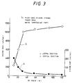
- a microwave plasma etching apparatus was used as the etching apparatus, and etching was conducted under conditions of a gas pressure of 0.67 Pa (5 mTorr), an input power of 280 W and an RF bias of 30 W.
- a gas pressure of 0.67 Pa (5 mTorr) 0.67 Pa
- an input power of 280 W 0.67 W
- an RF bias of 30 W 0.67 Pa
- the lateral etching rate and the vertical etching rate were 0.1 ⁇ m/min and 1 ⁇ m/min, respectively
- the lateral etching rate and the vertical etching rate were 0.05 ⁇ m/min and 1 ⁇ m/min, respectively.
- the dependency of the etching rate upon the bias power was as shown in Fig. 3.
- a deep channel for isolation or channel capacitor could be formed on a silicon substrate by etching the silicon substrate through proper selection of the temperature ranging from -130 to -40°C. That is, according to the present invention, a deep channel having a Y-shaped cross section in which the sidewall of the upper part is inclined at an angle larger than that of the lower part. This made it very easy to fill an insulating material or polysilicon within the deep channel, so that the reliability of the semiconductor device was remarkably improved. It is noted that SF6 is preferably used as the etching gas.
- etching of a photoresist film was conducted by O2 plasma at a temperature selected from a range of 0 to -100°C.
- the inclination of the sidewall could be controlled within an angle range of 60° to 90°, and a photoresist pattern having a desired cross section could be formed.
- etching gas and wafer temperature may properly be selected according to the materials to be etched.
- a magnetron plasma etching apparatus may also be used besides the two above-described apparatuses.
Landscapes
- Drying Of Semiconductors (AREA)
- Internal Circuitry In Semiconductor Integrated Circuit Devices (AREA)
Claims (9)
- Procédé de corrosion à sec d'un article pour lui conférer une structure possédant une partie de paroi latérale inclinée, consistant à
placer l'article dans une chambre à réaction, mettre l'article en contact avec un plasma d'un gaz corrosif pour corroder une partie exposée de l'article, et
modifier la température de l'article pendant le processus de corrosion depuis une température de départ égale ou inférieure à 0°C jusqu'à une température finale qui est inférieure à la température de départ, ce qui permet de modifier le degré de corrosion latérale. - Procédé selon la revendication 1, dans lequel la température finale est inférieure d'au moins 10°C à la température de départ.
- Procédé selon la revendication 1 ou 2, dans lequel la modification de température est exécutée au moyen d'une commutation pas-à-pas depuis la température de départ jusqu'à la température finale.
- Procédé selon la revendication 3, dans lequel la partie de paroi latérale formée à la température finale est sensiblement perpendiculaire à la surface principale de l'article.
- Procédé selon l'une quelconque des revendications 1 à 4, dans lequel l'article devant être corrodé est une pellicule d'aluminium et le gaz corrosif est du Cl₂.
- Procédé selon l'une quelconque des revendications 1 à 4, dans lequel l'article devant être corrodé est une pellicule de polysilicium et le gaz corrosif est du SF₆.
- Procédé selon l'une quelconque des revendications 1 à 4, dans lequel l'article devant être corrodé est un substrat en silicium monocristallin et le gaz corrosif est du SF₆.
- Procédé selon la revendication 7, dans lequel on forme un sillon profond.
- Procédé selon l'une quelconque des revendications 1 à 8, dans lequel la corrosion est exécutée en utilisant un dispositif de corrosion à sec à plaques planes parallèles ou un dispositif de corrosion plasmatique à micro-ondes.
Applications Claiming Priority (2)
| Application Number | Priority Date | Filing Date | Title |
|---|---|---|---|
| JP62187535A JPS6432633A (en) | 1987-07-29 | 1987-07-29 | Taper etching method |
| JP187535/87 | 1987-07-29 |
Publications (3)
| Publication Number | Publication Date |
|---|---|
| EP0301335A2 EP0301335A2 (fr) | 1989-02-01 |
| EP0301335A3 EP0301335A3 (en) | 1989-05-24 |
| EP0301335B1 true EP0301335B1 (fr) | 1994-11-30 |
Family
ID=16207788
Family Applications (1)
| Application Number | Title | Priority Date | Filing Date |
|---|---|---|---|
| EP88111438A Expired - Lifetime EP0301335B1 (fr) | 1987-07-29 | 1988-07-15 | Procédé d'attaque sèche |
Country Status (5)
| Country | Link |
|---|---|
| US (1) | US4986877A (fr) |
| EP (1) | EP0301335B1 (fr) |
| JP (1) | JPS6432633A (fr) |
| KR (1) | KR910007539B1 (fr) |
| DE (1) | DE3852230T2 (fr) |
Cited By (1)
| Publication number | Priority date | Publication date | Assignee | Title |
|---|---|---|---|---|
| CN105355550A (zh) * | 2015-12-02 | 2016-02-24 | 中国科学院微电子研究所 | Iii族氮化物低损伤刻蚀方法 |
Families Citing this family (28)
| Publication number | Priority date | Publication date | Assignee | Title |
|---|---|---|---|---|
| US5316616A (en) * | 1988-02-09 | 1994-05-31 | Fujitsu Limited | Dry etching with hydrogen bromide or bromine |
| US5002631A (en) * | 1990-03-09 | 1991-03-26 | At&T Bell Laboratories | Plasma etching apparatus and method |
| US6008133A (en) | 1991-04-04 | 1999-12-28 | Hitachi, Ltd. | Method and apparatus for dry etching |
| US5474650A (en) * | 1991-04-04 | 1995-12-12 | Hitachi, Ltd. | Method and apparatus for dry etching |
| US5318667A (en) * | 1991-04-04 | 1994-06-07 | Hitachi, Ltd. | Method and apparatus for dry etching |
| JP3248222B2 (ja) * | 1991-06-18 | 2002-01-21 | ソニー株式会社 | ドライエッチング方法 |
| US5171393A (en) * | 1991-07-29 | 1992-12-15 | Moffat William A | Wafer processing apparatus |
| JP3412173B2 (ja) * | 1991-10-21 | 2003-06-03 | セイコーエプソン株式会社 | 半導体装置の製造方法 |
| US5269880A (en) * | 1992-04-03 | 1993-12-14 | Northern Telecom Limited | Tapering sidewalls of via holes |
| US5302238A (en) * | 1992-05-15 | 1994-04-12 | Micron Technology, Inc. | Plasma dry etch to produce atomically sharp asperities useful as cold cathodes |
| US5753130A (en) | 1992-05-15 | 1998-05-19 | Micron Technology, Inc. | Method for forming a substantially uniform array of sharp tips |
| US5302239A (en) * | 1992-05-15 | 1994-04-12 | Micron Technology, Inc. | Method of making atomically sharp tips useful in scanning probe microscopes |
| JP3502096B2 (ja) * | 1992-06-22 | 2004-03-02 | ラム リサーチ コーポレイション | プラズマ処理装置内の残留物を除去するためのプラズマクリーニング方法 |
| US5352327A (en) * | 1992-07-10 | 1994-10-04 | Harris Corporation | Reduced temperature suppression of volatilization of photoexcited halogen reaction products from surface of silicon wafer |
| JP2650178B2 (ja) * | 1992-12-05 | 1997-09-03 | ヤマハ株式会社 | ドライエッチング方法及び装置 |
| JP3349001B2 (ja) * | 1994-12-29 | 2002-11-20 | ソニー株式会社 | 金属膜の形成方法 |
| JPH08274073A (ja) * | 1995-03-31 | 1996-10-18 | Sony Corp | アルミニウム系金属膜のエッチング方法 |
| JPH0964366A (ja) * | 1995-08-23 | 1997-03-07 | Toshiba Corp | 薄膜トランジスタ |
| US5647953A (en) * | 1995-12-22 | 1997-07-15 | Lam Research Corporation | Plasma cleaning method for removing residues in a plasma process chamber |
| US5882535A (en) * | 1997-02-04 | 1999-03-16 | Micron Technology, Inc. | Method for forming a hole in a semiconductor device |
| US6582617B1 (en) * | 1997-02-28 | 2003-06-24 | Candescent Technologies Corporation | Plasma etching using polycarbonate mask and low-pressure high density plasma |
| US5849641A (en) * | 1997-03-19 | 1998-12-15 | Lam Research Corporation | Methods and apparatus for etching a conductive layer to improve yield |
| US6833280B1 (en) * | 1998-03-13 | 2004-12-21 | Micron Technology, Inc. | Process for fabricating films of uniform properties on semiconductor devices |
| US6077789A (en) * | 1998-07-14 | 2000-06-20 | United Microelectronics Corp. | Method for forming a passivation layer with planarization |
| US6770564B1 (en) * | 1998-07-29 | 2004-08-03 | Denso Corporation | Method of etching metallic thin film on thin film resistor |
| US6403423B1 (en) * | 2000-11-15 | 2002-06-11 | International Business Machines Corporation | Modified gate processing for optimized definition of array and logic devices on same chip |
| JP5499920B2 (ja) * | 2010-06-09 | 2014-05-21 | 住友電気工業株式会社 | 半導体光デバイスの製造方法 |
| CN117096173A (zh) * | 2022-05-12 | 2023-11-21 | 芯恩(青岛)集成电路有限公司 | 场氧化层及其形成方法 |
Family Cites Families (9)
| Publication number | Priority date | Publication date | Assignee | Title |
|---|---|---|---|---|
| JPS5690525A (en) * | 1979-11-28 | 1981-07-22 | Fujitsu Ltd | Manufacture of semiconductor device |
| JPS577936A (en) * | 1980-06-18 | 1982-01-16 | Fujitsu Ltd | Manufacture of semiconductor device |
| JPS6066823A (ja) * | 1983-09-22 | 1985-04-17 | Semiconductor Energy Lab Co Ltd | 半導体エッチング方法 |
| JPH0614518B2 (ja) * | 1984-01-27 | 1994-02-23 | 株式会社日立製作所 | 表面反応の制御方法 |
| JPS60169140A (ja) * | 1984-02-13 | 1985-09-02 | Hitachi Ltd | ドライエツチング方法 |
| US4639288A (en) * | 1984-11-05 | 1987-01-27 | Advanced Micro Devices, Inc. | Process for formation of trench in integrated circuit structure using isotropic and anisotropic etching |
| US4726879A (en) * | 1986-09-08 | 1988-02-23 | International Business Machines Corporation | RIE process for etching silicon isolation trenches and polycides with vertical surfaces |
| DE3752140T2 (de) * | 1986-09-05 | 1998-03-05 | Hitachi Ltd | Trockenes Ätzverfahren |
| JPS63238288A (ja) * | 1987-03-27 | 1988-10-04 | Fujitsu Ltd | ドライエツチング方法 |
-
1987
- 1987-07-29 JP JP62187535A patent/JPS6432633A/ja active Pending
-
1988
- 1988-07-15 DE DE3852230T patent/DE3852230T2/de not_active Expired - Fee Related
- 1988-07-15 EP EP88111438A patent/EP0301335B1/fr not_active Expired - Lifetime
- 1988-07-15 KR KR1019880008833A patent/KR910007539B1/ko not_active Expired
- 1988-07-25 US US07/223,642 patent/US4986877A/en not_active Expired - Fee Related
Cited By (2)
| Publication number | Priority date | Publication date | Assignee | Title |
|---|---|---|---|---|
| CN105355550A (zh) * | 2015-12-02 | 2016-02-24 | 中国科学院微电子研究所 | Iii族氮化物低损伤刻蚀方法 |
| CN105355550B (zh) * | 2015-12-02 | 2018-05-01 | 中国科学院微电子研究所 | Iii族氮化物低损伤刻蚀方法 |
Also Published As
| Publication number | Publication date |
|---|---|
| JPS6432633A (en) | 1989-02-02 |
| DE3852230D1 (de) | 1995-01-12 |
| KR890003004A (ko) | 1989-04-12 |
| US4986877A (en) | 1991-01-22 |
| EP0301335A2 (fr) | 1989-02-01 |
| DE3852230T2 (de) | 1995-04-06 |
| EP0301335A3 (en) | 1989-05-24 |
| KR910007539B1 (ko) | 1991-09-27 |
Similar Documents
| Publication | Publication Date | Title |
|---|---|---|
| US4986877A (en) | Method of dry etching | |
| US5035768A (en) | Novel etch back process for tungsten contact/via filling | |
| US4980018A (en) | Plasma etching process for refractory metal vias | |
| US6004863A (en) | Non-polishing sacrificial layer etchback planarizing method for forming a planarized aperture fill layer | |
| US6069091A (en) | In-situ sequential silicon containing hard mask layer/silicon layer plasma etch method | |
| US4943344A (en) | Etching method | |
| US4919748A (en) | Method for tapered etching | |
| US5354416A (en) | Dry etching method | |
| US5147500A (en) | Dry etching method | |
| US5160407A (en) | Low pressure anisotropic etch process for tantalum silicide or titanium silicide layer formed over polysilicon layer deposited on silicon oxide layer on semiconductor wafer | |
| EP0314990B1 (fr) | Procédé pour l'attaque préférentielle de silicium polycristallin | |
| US4791073A (en) | Trench isolation method for semiconductor devices | |
| US6117786A (en) | Method for etching silicon dioxide using fluorocarbon gas chemistry | |
| EP0256311A2 (fr) | Procédé RIE pour graver des rainures d'isolation à parois verticales dans du silicium et du polycide | |
| US5458734A (en) | Method of fabricating a semiconductor device | |
| US5188980A (en) | Inert gas purge for the multilayer poly gate etching improvement | |
| JP2531492B2 (ja) | 応力緩和形状のトレンチ隅部をsoiウエハ内に形成する方法 | |
| US5071788A (en) | Method for depositing tungsten on silicon in a non-self-limiting CVD process and semiconductor device manufactured thereby | |
| EP0536968A2 (fr) | Procédé de formation de trous de contact pendant la fabrication de composants semi-conducteurs | |
| US5705029A (en) | Dry etching method | |
| EP0328350B1 (fr) | Attaque sèche avec du bromure d'hydrogène ou du brome | |
| US4708767A (en) | Method for providing a semiconductor device with planarized contacts | |
| EP0148340A1 (fr) | Procédé de décapage par ions de rainures profondes dans des substrats semi-conducteurs multicouches | |
| US5651858A (en) | Method for forming a tapered opening in silicon | |
| US5643473A (en) | Dry etching method |
Legal Events
| Date | Code | Title | Description |
|---|---|---|---|
| PUAI | Public reference made under article 153(3) epc to a published international application that has entered the european phase |
Free format text: ORIGINAL CODE: 0009012 |
|
| AK | Designated contracting states |
Kind code of ref document: A2 Designated state(s): DE FR |
|
| PUAL | Search report despatched |
Free format text: ORIGINAL CODE: 0009013 |
|
| AK | Designated contracting states |
Kind code of ref document: A3 Designated state(s): DE FR |
|
| 17P | Request for examination filed |
Effective date: 19891027 |
|
| 17Q | First examination report despatched |
Effective date: 19920518 |
|
| GRAA | (expected) grant |
Free format text: ORIGINAL CODE: 0009210 |
|
| AK | Designated contracting states |
Kind code of ref document: B1 Designated state(s): DE FR |
|
| PG25 | Lapsed in a contracting state [announced via postgrant information from national office to epo] |
Ref country code: FR Effective date: 19941130 |
|
| REF | Corresponds to: |
Ref document number: 3852230 Country of ref document: DE Date of ref document: 19950112 |
|
| EN | Fr: translation not filed | ||
| PLBE | No opposition filed within time limit |
Free format text: ORIGINAL CODE: 0009261 |
|
| STAA | Information on the status of an ep patent application or granted ep patent |
Free format text: STATUS: NO OPPOSITION FILED WITHIN TIME LIMIT |
|
| 26N | No opposition filed | ||
| PGFP | Annual fee paid to national office [announced via postgrant information from national office to epo] |
Ref country code: DE Payment date: 19980928 Year of fee payment: 11 |
|
| PG25 | Lapsed in a contracting state [announced via postgrant information from national office to epo] |
Ref country code: DE Free format text: LAPSE BECAUSE OF NON-PAYMENT OF DUE FEES Effective date: 20000503 |