EP0301545A2 - Dispositif pour émettre des électrons à conduction superficielle - Google Patents
Dispositif pour émettre des électrons à conduction superficielle Download PDFInfo
- Publication number
- EP0301545A2 EP0301545A2 EP88112243A EP88112243A EP0301545A2 EP 0301545 A2 EP0301545 A2 EP 0301545A2 EP 88112243 A EP88112243 A EP 88112243A EP 88112243 A EP88112243 A EP 88112243A EP 0301545 A2 EP0301545 A2 EP 0301545A2
- Authority
- EP
- European Patent Office
- Prior art keywords
- electron
- potential electrode
- low
- surface conduction
- potential
- Prior art date
- Legal status (The legal status is an assumption and is not a legal conclusion. Google has not performed a legal analysis and makes no representation as to the accuracy of the status listed.)
- Granted
Links
Images


Classifications
-
- H—ELECTRICITY
- H01—ELECTRIC ELEMENTS
- H01J—ELECTRIC DISCHARGE TUBES OR DISCHARGE LAMPS
- H01J1/00—Details of electrodes, of magnetic control means, of screens, or of the mounting or spacing thereof, common to two or more basic types of discharge tubes or lamps
- H01J1/02—Main electrodes
- H01J1/30—Cold cathodes, e.g. field-emissive cathode
- H01J1/316—Cold cathodes, e.g. field-emissive cathode having an electric field parallel to the surface, e.g. thin film cathodes
-
- H—ELECTRICITY
- H01—ELECTRIC ELEMENTS
- H01J—ELECTRIC DISCHARGE TUBES OR DISCHARGE LAMPS
- H01J2201/00—Electrodes common to discharge tubes
- H01J2201/30—Cold cathodes
- H01J2201/316—Cold cathodes having an electric field parallel to the surface thereof, e.g. thin film cathodes
- H01J2201/3165—Surface conduction emission type cathodes
Definitions
- the present invention relates to an electron-emitting device, and more particularly to a surface conduction electron-emitting device that emits electrons when an electric current is flowed in a highly resistant thin film.
- This surface conduction electron-emitting device includes those employing a SnO2 (Sb) thin film developed by Elinson et al., those employing an Au thin film. (G. Dittmer, “Thin Solid Films", Vol. 9, p.317, 1972), those comprising an ITO thin film, (M. Hartwell and C.G. Fonstad, "IEEE Trans. ED Conf.”, p.519, 1975), and those comprising a carbon thin film [Hisaji Araki, "SHINKU” (Vacuum), Vol. 26, No. 1, p.22, 1983)
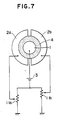
- a conventional surface conduction electron-emitting device comprises an insulating substrate 5 having thereon a highly resistant thin film 4 provided between a high-potential electrode 1 and a low-potential electrode 2, where a voltage is applied from an external electric source 3 and thereby electrons are emitted from the highly resistant thin film 4.
- an electron-emitting region 4 (a high-resistance thin film) by an energizing heat treatment, called "forming", before effecting the electron emission. More specifically, a voltage is applied between the above electrode 1 and electrode 2 to energize the thin film formed with an electron-emitting material to bring the thin film to be locally destroyed, deformed or denatured owing to the Joule heat thereby generated, thus forming the electron-emitting region 4 (a high-resistance thin film) kept in a state of electrically high resistance to obtain an electron-emitting function.
- An object of the present invention is to provide a surface conduction electron-emitting device that can solve the problems as mentioned above, caused by the insufficiency in the focusing performance, and can achieve a good beam-focusing performance without requiring any external focusing lenses 17 and 18.
- surface conduction electron-emitting device comprising a high-potential electrode provided on a substrate surface, an electron-emitting region provided in contact with the periphery of an exposed part of said high-potential electrode, and a low-potential electrode further provided in contact with the periphery of said electron-emitting region.
- a surface conduction electron-emitting device comprising a high-potential electrode provided on a substrate surface, an electron-emitting region provided in contact with the periphery of an exposed part of said high-potential electrode, and a low-potential electrode further provided in contact with the periphery of said electron-emitting region in such a manner that it projects upward in the thickness direction of the substrate to a higher level than the high-potential electrode.
- a surface conduction electron-emitting device comprising a high-potential electrode provided on a substrate surface, an electron-emitting region provided in contact with the periphery of an exposed part of said high-potential electrode, a low-potential electrode further provided in contact with the periphery of said electron-emitting region, and a means for applying a voltage between said high-potential electrode and low-potential electrode.
- a surface conduction electron-emitting device comprising a high-potential electrode provided on a substrate surface, an electron-emitting region provided in contact with the periphery of an exposed part of said high-potential electrode, a plurality of low-potential electrods provided in contact with the periphery of the electron-emitting region, and means for applying different potential independently to each of said low-potential electrodes.
- Fig. 1 is a basic block diagram illustrating an example of the surface conduction electron-emitting device of the present invention.
- the surface conduction electron-emitting device of the present invention comprises a pair of electrodes, of which a high-potential electrode 1 having a round shape and feeding an electric current to an electron- emitting region 4 is concentrically provided on its periphery with the electron-emitting region 4, and a low-potential electrode is similarly concentrically provided around the electron-emitting region 4.
- the potential is constant everywhere on the respective electrodes.
- the high-potential electrode 1 and the low-potential electrode 2 are separated right and left to form line symmetry, while in the device of the present invention illustrated in Fig. 1, the electrode form center symmetry and rotation symmetry to being about remarkably high symmetricalness as a whole.
- the velocity distribution of the electrons to be emitted may be neither irregular not deflected in contrast with the prior art, but can be uniform distribution having the center symmetricalness and rotation symmetricalness, so that the electron beam emitted from the surface conduction electron-emitting device can be focused at a particular position, i.e., a spot located at the direction perpendicular to the center of said device, and moreover decrease the flickering due to the substantial increase of the area of the light-emitting region.
- Fig. 2 is a view explanatory of how electrons emit from the surface conduction electron-emitting device of the present invention.
- Fig. 2 when a voltage is applied to an accelerating electric source 6, electrons tend to converge to the center as a whole as indicated by arrow A. This is because the potential distribution is generated such that the electrons are inclined to focus to the high-potential side at the center since the high-potential electrode 1 has a high potential and the low-potential electrode has a low potential. For this reason, a good focusing performance can be achieved when electrons are focused to a target electrode 9 with use of the accelerating electric source 6, even without providing any external focusing lenses such as lens electrodes 17 and 18 as illustrated in Fig. 19 of the prior art.
- such a surface conduction electron-emitting device of the present invention as having the structure that the electrodes 1 and 2 and focusing lenses 17 and 18 of the prior art have been integrated to the high-potential electrode 1 and low-potential electrode, makes it possible to bring the electrons to focus to a specific part, i.e. a vertically upper part of the center of said device.
- the electrodes and the electron-emitting region may not necessarily have the round shapes.
- the low-potential electrode is divided into a plural number of electrodes to provide a plural number of electron-emitting regions of curved or linear shapes, so long as the device basically comprises a high-potential electrode provided on a substrate surface, an electron-emitting region provided in contact with the periphery of an exposed part of said high-potential electrode, and a low-potential electrode further provided in contact with the periphery of said electron-emitting region.
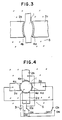
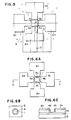
- the high-potential electrode may preferably have a round or oval shape (as exemplified by the devices having the electron-emitting region as illustrated in Fig. 1, 3 and 4). Also, in the instance where the electron-emitting region 4 is made to have the linear shape, the high-potential electrode 1 may preferably have a polygonal shape (as exemplified by those illustrated in Fig. 5).
- the device is so constituted that the low-potential electrodes 2b and 2d can be selected whether they work as low-potential electrodes (ON) or not (OFF), by means of a switch 10a, and, similarly, ON/OFF of the low-potential electrodes 2a and 2c can be selected by means of a switch 10b.
- electron-emitting regions 4b and 4d provided between the high-potential electrode 1 and the low-potential electrodes 2b and 2d constitutes one set of electron-emitting regions (referred to as Set I), and, similarly, 4a and 4c constitute one set (referred to as Set II).
- the ON/Off of the electron-emitting regions of Set I and that of the electron-emitting regions of Set II can be selected by the switch 10a and switch 10b, respectively. Accordingly, the switch 10b may be kept turn off and only switch 10a may be turned on to drive the surface conduction electron-emitting device of the present invention, so that there is given an electron-emitting device in which the center of the light-emitting region is positioned vertically above the center of the surface conduction electron-emitting device of the present invention and a space electron-emitting region is provided corresponding to Set II that makes provisions for the case when the electron-emitting regions of Set I turned impossible for use because of end of life of the electron-emitting regions.
- the surface conduction electron-emitting device of the present invention may also be a 'vertical type' surface conduction electron-emitting device comprising; a pair of electrodes 1 and 2b positioned on and beneath a stepped portion of a step-forming layer 15 provided on a substrate 12, said electrodes 1 and 2b oposing each other with said stepped portion between to have electrode spacing; and an electron-emitting region 4b formed at the side end face of the stepped portion positioned between said electrodes 1 and 2b; where electrons are emitted from the electron-emitting region 4b on applying a voltage between the electrodes 1 and 2b.
- the beam of emitted electrons can be brought to focus, so long as the device has the form, as illustrated in Fig. 6A, 6B and 6C, comprising a high-potential electrode 1 provided on a substrate surface, electron-emitting regions 4 and 4a to 4d provided in contact with the periphery of an exposed part of said high-potential electrode, and low-potential electrodes 2 and 2a to 2d further provided in contact with the peripheries of said electron-emitting regions 4 and 4a to 4d.
- the electron beam can also be brought to deflect to a desired direction by independently applying different potential to each of the low-potential electrodes.
- a low-potential electrode 2 is divided into two parts, 2a and 2b, to which potential Va, Vb is independently applied. Namely, if Va > Vb, the beam deflects toward 2a, and, in the reverse, it deflects toward 2b. In this occasion, the direction and magnitude of the deflection depends on Va minus Vb, and the amount of emitted electrons and the degree of focusing substantially depend on Va plus Vb. Accordingly, the both can be controlled independently. Additionally speaking, the low-potential electrode 2 need not be divided into two parts, and can be divided into desired number of electrodes according to what purpose the device is used for.
- the focusing performance of the electron beam can be more improved by providing a low-potential electrode in such a manner that it projects upward in the thickness direction of the substrate to a higher level than the high-potential electrode.
- the diameter d1 of the high-potential electrode 1 when the device takes the constitution that a high-potential electrode 1 has a round shape and is surrounded by a low-potential electrode forming a hole in between, the diameter d1 of the high-potential electrode 1, the diameter d2 of the hole defined by the low-potential electrode 2 and the height h of the hole (or the distance from the top surface of the high-potential electrode to the top surface of the low-potential electrode) may preferably satisfy the following relationship: d2 - d1 ⁇ 4 ⁇ m (a) d2/6 ⁇ h ⁇ 6 d2 (b)
- the numeral 1 denotes a high-potential electrode; 2, a low-potential electrode; and 4, an electron-emitting region.
- a plane target electrode to which a positive voltage of several to several ten kV has been applied is disposed above the surface conduction electron-emitting device.
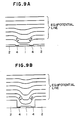
- Fig. 9A shows equipotential lines in the vicinity of a surface conduction electron emitting device comprising electrodes 1 and 2 both made equal in thickness, and the direction of a representative force exerted to the electron beam, which is indicated by arrows F.
- Fig. 9B shows a state in the vicinity of a surface conduction electron-emitting device comprising the low-potential electrode 2 projected upward in the thickness direction of the substrate to a higher level than the high-potential electrode 1.
- the slant of equipotential lines is greater in the case where the low-potential electrode 2 has a larger thickness than the high-potential electrode 1, as compared with that in Fig. 9A. Accordingly, the electron beam undergoes a greater focusing force toward the center at the emission initial stage in which it has a small magnitude of the velocity component toward the target electrode and is subject to influence by the electric field.
- the low-potential electrode is divided into a plural number of electrodes to provide a plural number of electron-emitting regions of curved or linear shapes, so long as the device comprises a high-potential electrode provided on a substrate surface, an electron-emitting region provided in contact with the periphery of an exposed part of said high-potential electrode, and a low-potential electrode further provided in contact with the periphery of said electron-emitting region in such a manner that it projects upward in the thickness direction of the substrate to a higher level than the high-potential electrode.
- unevenness as illustrated in Figs. 13A to 13C may further be made on at least one of the boundary between the low-potential electrode and the electron-emitting region and the boundary between the high-potential electrode and the electron-emitting region. Forming the boundary in such a shape makes stronger the local electric field desirably. Also, as illustrated in Fig. 13D, the low-potential electrode 2 can be made to have any desired outer side shape according to any conditions of arrangement or wiring.
- the surface conduction electron-emitting device according to the present invention may also constitute a plural number of devices arranged on the same substrate and driven independently, so that there can be obtained a plural number of independent electron beams.
- Figs. 15A to 15E the surface of a substrate 16 is first oxidized to form an insulating film, thus preparing an insulating substrate 5 (Fig. 15A).
- Fig. 15B part of the insulating substrate 5 is etched to make a hole, and thereafter a metal film 20 is formed on the whole surface by vapor deposition (Fig. 15B).
- This metal film 20 is further etched as illustrated in Fig. 15C to prepare a high-potential electrode 1 and low-potential electrodes 2a and 2c.
- a thin film 21 is formed by vapor deposition, and then a forming treatment is carried out (Fig. 15D).
- the thin film adheres also on top surfaces of these, but this does not affect the characteristics of the device in practical use. If necessary, however, it is of course possible to cover with a mask the top surfaces of the high-potential electrode 1 and low-potential electrodes 2a and 2c to prevent the thin film from adhering thereon.
- application of a voltage between the low-potential electrodes 2a and 2c and the substrate 16 from an external electric source 3 brings about emission of electrons from electron-emitting regions 4a and 4c (Fig. 15E).
- a wiring electrode 14 is first patterned in the shape of a stripe on a substrate 12 made of glass, quartz or the like (Fig. 16A).
- an insulating layer 13 is formed on the substrate 12 and wiring electrode 14 (Fig. 16B), and this insulating layer 13 is worked to make a hole by etching as illustrated in Fig. 16C.
- a metal film is formed by vapor deposition, followed by etching to prepare a high-potential electrode 1 (Fig. 16 D).
- a thin film 4 is further formed by vapor deposition and a forming treatment is carried out (Fig. 16E).
- a metal film 2 that formed the high-potential electrode 1 is formed by vapor deposition (Fig. 16F), followed by working to make a hole by etching to prepare low-potential electrode 2a and 2c (Fig. 16G).
- electron-emitting regions 4a and 4c are formed by vapor deposition, but, without limitation thereto, also available is a method in which a dispersion obtained by dispersing fine particles of an electron-emitting material in a dispersion medium is applied by, for example, dipping or spin coating, followed by baking.
- the dispersion medium may be any of those capable of dispersing the fine particles without any change of their properties, and there may be used, for example, alcohols, methyl ethyl ketone, cyclohexane, and a mixture of any of these.
- the fine particles may preferably have a particle diameter of several ten angstroms to several um.
- Materials for constituting the surface conduction electron-emitting device of the present invention may be any of those used in conventional surface conduction electron-emitting devices.
- the substrate 16 (Fig. 15) may be made of any materials so long as they are electroconductive, including n-type Si, P-Si, or metals such as Al and Cu.
- the high-potential electrode 1 and low-potential electrodes 2a and 2c (Figs. 15 and 16), and also the wiring electrode 14 (Fig. 16) may also be made of any materials so long as they are good conductors, and there can be used, for example, metals such as Cu, Pb, Ni, Al, Au, Pt and Ag, and oxides such as SnO2 and ITO.
- the insulating substrate 5 may also be made of any materials so long as the insulating film formed thereon comprises an insulator, but what can be simple in view of preparation methods may preferably include SiO2 and Al2O3 obtainable by oxidation of the substrate. Insulators such As SiO2, MgO and glass are also used in the substrate 12 and insulating layer 13 (Fig. 16).
- metal oxides such as as In2O3, SnO2 and PbO
- metals such as Ag, Pt, Al, Cu and Au
- carbon and other various semiconductors.
- the high-potential electrode 1 may be made to have a size of from 1 nm to several mm, the electron-emitting regions 4a and 4c may each have a width of the size corresponding to that of a conventional surface conduction electron-emitting device (for example, 1 ⁇ m to several ten mm), and the low-potential electrodes 2a and 2c may have any size.
- the electron-emitting regions 4a and 4c may also each have a thickness corresponding to that of a conventional surface conduction electron-emitting device (for example, several ten ⁇ to several ⁇ m).
- the high-potential electrode 1 and the low-potential electrodes 2a and 2c may have any thickness. Since, however, an excessively large thickness may cause hindrance of electron emission, the high-potential electrode 1 may desirably have a little larger thickness than the film thickness of the electron-emitting regions.
- the insulating substrate may have any thickness.
- the low-potential electrodes 2a and 2c are formed to have a larger thickness than the high-potential electrode 1, in order to they improve the electron beam focusing, should be formed so as to satisfy the relationship of the formulas (a) and (b) previously described.
- the wiring electrode 14 may be formed on the substrate 12 by patterning to have a desired shape such as a stripe on a desired position and then the high-potential electrode 1 may be provided on this wiring electrode 14 as shown in Figs. 16, thus preferably making easy the manufacture.
- an insulating material is used in general as the step-forming layer 15 as illustrated in Fig. 6C and Fig. 12C.
- the material may be SiO2, MgO, TiO2, Ta2O5 and Al2O3, a laminate of any of these, or a mixture of any of these.
- the spacing between the electrodes 1 and 2 depends on the thickness of the step-forming layer 15 and the thickness of the electrodes 1 and 2, but may preferably be several ten angstroms to several um.
- Other component members may employ the same materials and constitution as those previously described.
- the surface conduction electron-emitting device of the present invention comprises a high-potential electrode provided on a substrate surface, an electron-emitting region provided in contact with the periphery of an exposed part of said high-potential electrode, and a low-potential electrode further provided in contact with the periphery of said electron-emitting region. It is possible to focus the electron beam to a particular position, i.e., a spot located at the direction perpendicular to the center of said device, and moreover decrease the flickering at the light-emitting region.
- the low-potential electrode of said device is divided into a plural number of electrodes to provide a plural number of electron-emitting regions, it is possible for the surface conduction electron-emitting device of the present invention to be provided with a spare electron-emitting region.
- the surface conduction electron-emitting device of the present invention when taking the constitution comprising an inside high-potential electrode and an outside low-potential electrode projecting upward in the thickness direction of a substrate, can further enhance the beam-focusing performance, make smaller the size of the electron beam on a target electrode, and make it unnecessary to provide any external focusing lenses.
- a surface conduction electron-emitting device was prepared in a manner shown in figs. 15A to 15E.
- the surface of an n-type Si substrate was oxidized to form an insulating film comprising SiO2, and part thereof was etched to make a hole, followed by vapor deposition of an Al metal film on the whole surface.
- the resulting deposited film was further etched to prepared high-potential and low-potential electrodes.
- a thin Au film was further formed thereon by vapor deposition, and a forming treatment was carried out, thus obtaining the surface conduction electron-emitting devices illustrated each in Fig. 1 and Fig. 5.
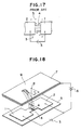
- the surface conduction electron-emitting device of the present invention showed about 1/2 flicker as compared with 16 % flicker in the conventional device (Fig. 17), and the center of the light-emitting spot was positioned at the direction perpendicular to the center of the surface conduction electron-emitting device.
- Example 1 was repeated to prepare the surface conduction electron-emitting device illustrated in Fig. 3.
- the flickering at the light-emitting region thereof was 1/1.4 of that in the prior art.
- the center of the light-emitting spot was also positioned at the direction perpendicular to the center of the device.
- Example 1 was repeated to prepare the surface conduction electron-emitting device illustrated in Fig. 4.
- the flickering at the light-emitting region thereof was 1/1.4 of that in the prior art.
- the center of the light-emitting spot was also positioned at the direction perpendicular to the center of the device.
- a surface conduction electron-emitting device was prepared in a manner shown in Figs. 16A to 16G.
- the numeral 12 denotes a glass substrate
- 14 denotes a wiring electrode which is provided in a stripe pattern on the substrate 12.
- the material for the wiring electrode 14 was comprised of a laminate of Cr of 50 angstroms thick and Ta of 1,000 angstroms thick.
- the numeral 13 denotes an insulating layer, which was formed by coating a liquid SiO2 coating preparation (OCD, available from Tokyo Ohka Kogyo) to a thickness of 1 micron.
- OCD liquid SiO2 coating preparation
- Photolithoetching was conducted to make a hole in the insulating layer 13, followed by deposition of Cu to a thickness of 1.2 ⁇ m thereon, and the copper other than that necessary for the high-potential electrode 1 was removed by photolithoetching.
- a solution of an organic palladium compound (Catapaste CCP, available from Okuno Seiyaku Kogyo) was applied thereon by spinner coating. Thereafter, the coating was baked for 1 hour at 400°C to prepare a thin film 4 having a film thickness of 1,500 angstroms and containing Pd fine particles.
- Catapaste CCP available from Okuno Seiyaku Kogyo
- a low-potential electrode 2 Al was vapor deposited to a thickness of 10 ⁇ m, and, as shown in Fig. 8A and Fig. 8B, the peripheral area of the high potential electrode 1 was removed by conventional photolithoetching. At the same time, the low-potential electrode 2 was etched to give the shape of a stripe serving also as a wiring electrode.
- the diameter d1 of the high-potential electrode 1, the diameter d2 of the hole of the low-potential electrode 2, and the height h thereof were made to have the following relationship: d1 ⁇ 10 ⁇ m d2 ⁇ 14 ⁇ m h ⁇ 10 ⁇ m
- the surface conduction electron-emitting device As in the above, placed was a target electrode coated with a phosphor and applied with an accelerated voltage, and the spreading of the electron beam was measured. As a result, it was confirmed that the spreading was about 3/5 with a remarkable enhancement of the focusing performance, as compared with a surface conduction electron emitting device comprising electrodes 1 and 2 both made equal in thickness.
- the device was made to have the same structure as in Example 4 except that the high-potential electrode 1 was held between two thick low-potential electrodes 2a and 2b from the both sides.
- the device was made to have the same structure as in Example 4 except that the high-potential electrode 1 was surrounded by four thick low-potential electrodes 2a to 2d.
Landscapes
- Cold Cathode And The Manufacture (AREA)
- Cathode-Ray Tubes And Fluorescent Screens For Display (AREA)
Applications Claiming Priority (6)
| Application Number | Priority Date | Filing Date | Title |
|---|---|---|---|
| JP186648/87 | 1987-07-28 | ||
| JP18664887 | 1987-07-28 | ||
| JP14156288 | 1988-06-10 | ||
| JP141563/88 | 1988-06-10 | ||
| JP14156388 | 1988-06-10 | ||
| JP141562/88 | 1988-06-10 |
Publications (3)
| Publication Number | Publication Date |
|---|---|
| EP0301545A2 true EP0301545A2 (fr) | 1989-02-01 |
| EP0301545A3 EP0301545A3 (en) | 1990-08-01 |
| EP0301545B1 EP0301545B1 (fr) | 1996-01-10 |
Family
ID=27318273
Family Applications (1)
| Application Number | Title | Priority Date | Filing Date |
|---|---|---|---|
| EP88112243A Expired - Lifetime EP0301545B1 (fr) | 1987-07-28 | 1988-07-28 | Dispositif pour émettre des électrons à conduction superficielle |
Country Status (4)
| Country | Link |
|---|---|
| US (1) | US4956578A (fr) |
| EP (1) | EP0301545B1 (fr) |
| JP (1) | JP2704731B2 (fr) |
| DE (1) | DE3854882T2 (fr) |
Cited By (8)
| Publication number | Priority date | Publication date | Assignee | Title |
|---|---|---|---|---|
| EP0312007A3 (en) * | 1987-10-12 | 1990-04-18 | Canon Kabushiki Kaisha | Electron beam emitting device and image displaying device by use thereof |
| EP0619594A1 (fr) * | 1993-04-05 | 1994-10-12 | Canon Kabushiki Kaisha | Source d'électrons et appareil de formation d'images |
| EP0658924A1 (fr) * | 1993-12-17 | 1995-06-21 | Canon Kabushiki Kaisha | Procédé de fabrication d'un dispositif émitteur d'électrons, une source d'électrons et un dispositif de formation d'images |
| EP0658912A1 (fr) * | 1993-12-14 | 1995-06-21 | Canon Kabushiki Kaisha | Source d'électrons et dispositif de formation d'images, et procédé de fabrication |
| EP0675517A1 (fr) * | 1994-03-29 | 1995-10-04 | Canon Kabushiki Kaisha | Source d'électrons et dispositif de formation d'images |
| EP0805472A1 (fr) * | 1996-04-30 | 1997-11-05 | Canon Kabushiki Kaisha | Dispositif émetteur d'électrons, appareil de formation d'images en faisant usage et son procédé de fabrication |
| US6313815B1 (en) | 1991-06-06 | 2001-11-06 | Canon Kabushiki Kaisha | Electron source and production thereof and image-forming apparatus and production thereof |
| CN1086053C (zh) * | 1992-12-29 | 2002-06-05 | 佳能株式会社 | 电子源和图像形成装置 |
Families Citing this family (34)
| Publication number | Priority date | Publication date | Assignee | Title |
|---|---|---|---|---|
| JP2826549B2 (ja) | 1989-05-12 | 1998-11-18 | キヤノン株式会社 | 電子放出素子及び画像形成装置 |
| DE69027960T2 (de) * | 1989-09-04 | 1997-01-09 | Canon Kk | Elektronen emittierendes Element und Verfahren zur Herstellung desselben |
| EP0416625B1 (fr) * | 1989-09-07 | 1996-03-13 | Canon Kabushiki Kaisha | Dispositif émetteur d'électrons et son procédé de fabrication, dispositif d'affichage et d'écriture par faisceau d'électrons utilisant ledit dispositif. |
| JP2992894B2 (ja) | 1990-03-14 | 1999-12-20 | キヤノン株式会社 | 画像表示装置 |
| US5470265A (en) * | 1993-01-28 | 1995-11-28 | Canon Kabushiki Kaisha | Multi-electron source, image-forming device using multi-electron source, and methods for preparing them |
| JPH0536369A (ja) * | 1990-09-25 | 1993-02-12 | Canon Inc | 電子ビーム装置及びその駆動方法 |
| JPH04324231A (ja) * | 1991-04-24 | 1992-11-13 | Mitsubishi Electric Corp | 平面型表示装置 |
| US5455597A (en) * | 1992-12-29 | 1995-10-03 | Canon Kabushiki Kaisha | Image-forming apparatus, and designation of electron beam diameter at image-forming member in image-forming apparatus |
| US6005333A (en) * | 1993-05-05 | 1999-12-21 | Canon Kabushiki Kaisha | Electron beam-generating device, and image-forming apparatus and recording apparatus employing the same |
| ATE165187T1 (de) * | 1993-11-09 | 1998-05-15 | Canon Kk | Bildanzeigegerät |
| CA2138363C (fr) * | 1993-12-22 | 1999-06-22 | Yasuyuki Todokoro | Dispositif generateur de faisceau electronique, dispositif d'affichage d'images et methode d'attaque de ces dispositifs |
| JP3251466B2 (ja) | 1994-06-13 | 2002-01-28 | キヤノン株式会社 | 複数の冷陰極素子を備えた電子線発生装置、並びにその駆動方法、並びにそれを応用した画像形成装置 |
| US6246168B1 (en) * | 1994-08-29 | 2001-06-12 | Canon Kabushiki Kaisha | Electron-emitting device, electron source and image-forming apparatus as well as method of manufacturing the same |
| US5996488A (en) * | 1994-11-25 | 1999-12-07 | Canon Kabushiki Kaisha | Preparation of an electron source by offset printing electrodes having thickness less than 200 nm |
| JPH0981977A (ja) * | 1995-07-10 | 1997-03-28 | Canon Inc | 記録再生装置 |
| JP3311246B2 (ja) | 1995-08-23 | 2002-08-05 | キヤノン株式会社 | 電子発生装置、画像表示装置およびそれらの駆動回路、駆動方法 |
| US6621475B1 (en) | 1996-02-23 | 2003-09-16 | Canon Kabushiki Kaisha | Electron generating apparatus, image forming apparatus, method of manufacturing the same and method of adjusting characteristics thereof |
| JP3025249B2 (ja) | 1997-12-03 | 2000-03-27 | キヤノン株式会社 | 素子の駆動装置及び素子の駆動方法及び画像形成装置 |
| JP3535832B2 (ja) * | 1999-03-02 | 2004-06-07 | キヤノン株式会社 | 電子線放出装置及び画像形成装置 |
| JP2001229808A (ja) * | 1999-12-08 | 2001-08-24 | Canon Inc | 電子放出装置 |
| JP3658342B2 (ja) | 2000-05-30 | 2005-06-08 | キヤノン株式会社 | 電子放出素子、電子源及び画像形成装置、並びにテレビジョン放送表示装置 |
| JP3639808B2 (ja) | 2000-09-01 | 2005-04-20 | キヤノン株式会社 | 電子放出素子及び電子源及び画像形成装置及び電子放出素子の製造方法 |
| JP3639809B2 (ja) * | 2000-09-01 | 2005-04-20 | キヤノン株式会社 | 電子放出素子,電子放出装置,発光装置及び画像表示装置 |
| JP3658346B2 (ja) | 2000-09-01 | 2005-06-08 | キヤノン株式会社 | 電子放出素子、電子源および画像形成装置、並びに電子放出素子の製造方法 |
| JP3610325B2 (ja) | 2000-09-01 | 2005-01-12 | キヤノン株式会社 | 電子放出素子、電子源及び画像形成装置の製造方法 |
| JP3634781B2 (ja) * | 2000-09-22 | 2005-03-30 | キヤノン株式会社 | 電子放出装置、電子源、画像形成装置及びテレビジョン放送表示装置 |
| JP3768908B2 (ja) * | 2001-03-27 | 2006-04-19 | キヤノン株式会社 | 電子放出素子、電子源、画像形成装置 |
| JP3703415B2 (ja) * | 2001-09-07 | 2005-10-05 | キヤノン株式会社 | 電子放出素子、電子源及び画像形成装置、並びに電子放出素子及び電子源の製造方法 |
| JP3605105B2 (ja) * | 2001-09-10 | 2004-12-22 | キヤノン株式会社 | 電子放出素子、電子源、発光装置、画像形成装置および基板の各製造方法 |
| JP5665305B2 (ja) * | 2008-12-25 | 2015-02-04 | キヤノン株式会社 | 分析装置 |
| JP5936374B2 (ja) * | 2011-02-15 | 2016-06-22 | キヤノン株式会社 | 圧電振動型力センサ及びロボットハンド並びにロボットアーム |
| JP6335460B2 (ja) | 2013-09-26 | 2018-05-30 | キヤノン株式会社 | ロボットシステムの制御装置及び指令値生成方法、並びにロボットシステムの制御方法 |
| JP6964989B2 (ja) | 2017-02-09 | 2021-11-10 | キヤノン株式会社 | 制御方法、ロボットシステム、物品の製造方法、プログラム、及び記録媒体 |
| EP3366433B1 (fr) | 2017-02-09 | 2022-03-09 | Canon Kabushiki Kaisha | Procédé de commande d'un robot, procédé d'apprentissage d'un robot et système de robot |
Family Cites Families (8)
| Publication number | Priority date | Publication date | Assignee | Title |
|---|---|---|---|---|
| US3978364A (en) * | 1974-07-24 | 1976-08-31 | The United States Of America As Represented By The Administrator Of The National Aeronautics And Space Administration | Integrated structure vacuum tube |
| JPS56167456U (fr) * | 1980-05-16 | 1981-12-11 | ||
| SU1003195A1 (ru) * | 1981-10-26 | 1983-03-07 | Московский автомеханический институт | Ненакаливаемый катод |
| DE3538175C2 (de) * | 1984-11-21 | 1996-06-05 | Philips Electronics Nv | Halbleiteranordnung zum Erzeugen eines Elektronenstromes und ihre Verwendung |
| US4810934A (en) * | 1986-05-20 | 1989-03-07 | Canon Kabushiki Kaisha | Electron emission device |
| JPS634532A (ja) * | 1986-06-25 | 1988-01-09 | Canon Inc | 電子放出素子 |
| JP2760395B2 (ja) * | 1986-06-26 | 1998-05-28 | キヤノン株式会社 | 電子放出装置 |
| JP2518833B2 (ja) | 1987-01-28 | 1996-07-31 | キヤノン株式会社 | 電子放出装置 |
-
1988
- 1988-07-27 JP JP18549588A patent/JP2704731B2/ja not_active Expired - Lifetime
- 1988-07-27 US US07/224,912 patent/US4956578A/en not_active Expired - Lifetime
- 1988-07-28 EP EP88112243A patent/EP0301545B1/fr not_active Expired - Lifetime
- 1988-07-28 DE DE3854882T patent/DE3854882T2/de not_active Expired - Lifetime
Cited By (21)
| Publication number | Priority date | Publication date | Assignee | Title |
|---|---|---|---|---|
| EP0628982A3 (fr) * | 1987-10-12 | 1995-03-01 | Canon Kk | Procédé de commande d'un dispositif émitteur d'électrons. |
| EP0312007A3 (en) * | 1987-10-12 | 1990-04-18 | Canon Kabushiki Kaisha | Electron beam emitting device and image displaying device by use thereof |
| US6313815B1 (en) | 1991-06-06 | 2001-11-06 | Canon Kabushiki Kaisha | Electron source and production thereof and image-forming apparatus and production thereof |
| CN1086053C (zh) * | 1992-12-29 | 2002-06-05 | 佳能株式会社 | 电子源和图像形成装置 |
| CN1086054C (zh) * | 1993-04-05 | 2002-06-05 | 佳能株式会社 | 电子源和成象装置 |
| EP0619594A1 (fr) * | 1993-04-05 | 1994-10-12 | Canon Kabushiki Kaisha | Source d'électrons et appareil de formation d'images |
| US6313571B1 (en) | 1993-04-05 | 2001-11-06 | Canon Kabushiki Kaisha | Electron source and image-forming apparatus |
| US6409566B1 (en) | 1993-04-05 | 2002-06-25 | Canon Kabushiki Kaisha | Method of manufacturing an electron source and image forming apparatus using the same |
| US5912531A (en) * | 1993-04-05 | 1999-06-15 | Canon Kabushiki Kaisha | Electron source and image-forming apparatus |
| EP0658912A1 (fr) * | 1993-12-14 | 1995-06-21 | Canon Kabushiki Kaisha | Source d'électrons et dispositif de formation d'images, et procédé de fabrication |
| AU698650B2 (en) * | 1993-12-14 | 1998-11-05 | Canon Kabushiki Kaisha | Electron source and production thereof, and image-forming apparatus and production thereof |
| EP0658924A1 (fr) * | 1993-12-17 | 1995-06-21 | Canon Kabushiki Kaisha | Procédé de fabrication d'un dispositif émitteur d'électrons, une source d'électrons et un dispositif de formation d'images |
| AU687926B2 (en) * | 1993-12-17 | 1998-03-05 | Canon Kabushiki Kaisha | Method of manufacturing electron-emitting device, electron source and image-forming apparatus |
| US5622634A (en) * | 1993-12-17 | 1997-04-22 | Canon Kabushiki Kaisha | Method of manufacturing electron-emitting device, electron source and image-forming apparatus |
| EP0675517A1 (fr) * | 1994-03-29 | 1995-10-04 | Canon Kabushiki Kaisha | Source d'électrons et dispositif de formation d'images |
| CN1060881C (zh) * | 1994-03-29 | 2001-01-17 | 佳能株式会社 | 电子源和成象装置 |
| US6144166A (en) * | 1994-03-29 | 2000-11-07 | Canon Kabushiki Kaisha | Electron source and image-forming apparatus with a matrix array of electron-emitting elements |
| US5932963A (en) * | 1994-03-29 | 1999-08-03 | Canon Kabushiki Kaisha | Electron source and image-forming apparatus with a matrix array of electron-emitting elements |
| US6259191B1 (en) | 1996-04-30 | 2001-07-10 | Canon Kabushiki Kaisha | Electron-emitting apparatus having a periodical electron-emitting region |
| US6005334A (en) * | 1996-04-30 | 1999-12-21 | Canon Kabushiki Kaisha | Electron-emitting apparatus having a periodical electron-emitting region |
| EP0805472A1 (fr) * | 1996-04-30 | 1997-11-05 | Canon Kabushiki Kaisha | Dispositif émetteur d'électrons, appareil de formation d'images en faisant usage et son procédé de fabrication |
Also Published As
| Publication number | Publication date |
|---|---|
| EP0301545B1 (fr) | 1996-01-10 |
| DE3854882T2 (de) | 1996-08-14 |
| EP0301545A3 (en) | 1990-08-01 |
| JP2704731B2 (ja) | 1998-01-26 |
| DE3854882D1 (de) | 1996-02-22 |
| JPH02112125A (ja) | 1990-04-24 |
| US4956578A (en) | 1990-09-11 |
Similar Documents
| Publication | Publication Date | Title |
|---|---|---|
| EP0301545B1 (fr) | Dispositif pour émettre des électrons à conduction superficielle | |
| US5530314A (en) | Electron-emitting device and electron beam-generating apparatus and image-forming apparatus employing the device | |
| US5757123A (en) | Electron-beam generator and image display apparatus making use of it | |
| US5759080A (en) | Display device with electron-emitting device with electron-emitting region insulated form electrodes | |
| EP0628982B1 (fr) | Procédé de commande pour des dispositifs émetteurs de faisceaux d'électrons | |
| KR20010039952A (ko) | 전계 방출 디바이스 | |
| JPH0612997A (ja) | 電子放出素子及びその製造方法並びに該電子放出素子を用いた画像形成装置 | |
| JP2631007B2 (ja) | 電子放出素子及びその製造方法と、該素子を用いた画像形成装置 | |
| JP3168353B2 (ja) | 画像表示装置 | |
| KR100378103B1 (ko) | 전자원, 화상 형성 장치 및 전자원 제조 방법 | |
| JP2630990B2 (ja) | 電子放出素子及びそれを用いた発光素子 | |
| USRE39633E1 (en) | Display device with electron-emitting device with electron-emitting region insulated from electrodes | |
| JP2617317B2 (ja) | 電子線発生装置 | |
| USRE40062E1 (en) | Display device with electron-emitting device with electron-emitting region insulated from electrodes | |
| JP2961477B2 (ja) | 電子放出素子、電子線発生装置及び画像形成装置の製造方法 | |
| JP2992902B2 (ja) | 電子線発生装置 | |
| JP2850014B2 (ja) | 画像形成装置 | |
| JP3131752B2 (ja) | 電子放出素子、電子線発生装置及び画像形成装置並びにそれらの製造方法 | |
| JP2835962B2 (ja) | 画像形成装置 | |
| JP2916807B2 (ja) | 電子放出素子、電子源、画像形成装置及び、それらの製造方法 | |
| JP2715314B2 (ja) | 画像形成装置及びその駆動方法 | |
| JP2981503B2 (ja) | 電子放出素子、電子源及び画像表示装置 | |
| JP2961523B2 (ja) | 電子放出素子、電子源及び画像形成装置 | |
| JP2976135B2 (ja) | 電子線発生装置及びそれを用いた画像形成装置と光信号供与装置 | |
| JP3010296B2 (ja) | 画像形成装置 |
Legal Events
| Date | Code | Title | Description |
|---|---|---|---|
| PUAI | Public reference made under article 153(3) epc to a published international application that has entered the european phase |
Free format text: ORIGINAL CODE: 0009012 |
|
| AK | Designated contracting states |
Kind code of ref document: A2 Designated state(s): DE FR GB NL |
|
| PUAL | Search report despatched |
Free format text: ORIGINAL CODE: 0009013 |
|
| AK | Designated contracting states |
Kind code of ref document: A3 Designated state(s): DE FR GB NL |
|
| 17P | Request for examination filed |
Effective date: 19901214 |
|
| 17Q | First examination report despatched |
Effective date: 19930716 |
|
| GRAA | (expected) grant |
Free format text: ORIGINAL CODE: 0009210 |
|
| AK | Designated contracting states |
Kind code of ref document: B1 Designated state(s): DE FR GB NL |
|
| REF | Corresponds to: |
Ref document number: 3854882 Country of ref document: DE Date of ref document: 19960222 |
|
| ET | Fr: translation filed | ||
| PLBE | No opposition filed within time limit |
Free format text: ORIGINAL CODE: 0009261 |
|
| STAA | Information on the status of an ep patent application or granted ep patent |
Free format text: STATUS: NO OPPOSITION FILED WITHIN TIME LIMIT |
|
| 26N | No opposition filed | ||
| REG | Reference to a national code |
Ref country code: GB Ref legal event code: IF02 |
|
| PGFP | Annual fee paid to national office [announced via postgrant information from national office to epo] |
Ref country code: DE Payment date: 20070726 Year of fee payment: 20 |
|
| PGFP | Annual fee paid to national office [announced via postgrant information from national office to epo] |
Ref country code: GB Payment date: 20070725 Year of fee payment: 20 |
|
| PGFP | Annual fee paid to national office [announced via postgrant information from national office to epo] |
Ref country code: NL Payment date: 20070715 Year of fee payment: 20 |
|
| PGFP | Annual fee paid to national office [announced via postgrant information from national office to epo] |
Ref country code: FR Payment date: 20070710 Year of fee payment: 20 |
|
| REG | Reference to a national code |
Ref country code: GB Ref legal event code: PE20 Expiry date: 20080727 |
|
| NLV7 | Nl: ceased due to reaching the maximum lifetime of a patent |
Effective date: 20080728 |
|
| PG25 | Lapsed in a contracting state [announced via postgrant information from national office to epo] |
Ref country code: NL Free format text: LAPSE BECAUSE OF EXPIRATION OF PROTECTION Effective date: 20080728 |
|
| PG25 | Lapsed in a contracting state [announced via postgrant information from national office to epo] |
Ref country code: GB Free format text: LAPSE BECAUSE OF EXPIRATION OF PROTECTION Effective date: 20080727 |