EP0301794A1 - Dynamischer Speicher mit wahlfreiem Zugriff und mit Selbstauffrischungsfunktion - Google Patents
Dynamischer Speicher mit wahlfreiem Zugriff und mit Selbstauffrischungsfunktion Download PDFInfo
- Publication number
- EP0301794A1 EP0301794A1 EP88306838A EP88306838A EP0301794A1 EP 0301794 A1 EP0301794 A1 EP 0301794A1 EP 88306838 A EP88306838 A EP 88306838A EP 88306838 A EP88306838 A EP 88306838A EP 0301794 A1 EP0301794 A1 EP 0301794A1
- Authority
- EP
- European Patent Office
- Prior art keywords
- refreshing
- self
- clock
- circuit
- error
- Prior art date
- Legal status (The legal status is an assumption and is not a legal conclusion. Google has not performed a legal analysis and makes no representation as to the accuracy of the status listed.)
- Granted
Links
- 230000015654 memory Effects 0.000 claims abstract description 63
- 238000001514 detection method Methods 0.000 claims abstract description 42
- 230000006870 function Effects 0.000 claims abstract description 17
- 230000009471 action Effects 0.000 claims abstract description 9
- 230000003247 decreasing effect Effects 0.000 claims abstract description 6
- 239000011159 matrix material Substances 0.000 claims description 19
- 230000007257 malfunction Effects 0.000 abstract description 4
- 230000008859 change Effects 0.000 abstract description 3
- 238000004519 manufacturing process Methods 0.000 abstract description 3
- 238000010276 construction Methods 0.000 abstract 1
- 238000010586 diagram Methods 0.000 description 11
- 230000007423 decrease Effects 0.000 description 9
- 239000003990 capacitor Substances 0.000 description 7
- 230000001360 synchronised effect Effects 0.000 description 2
- 230000008094 contradictory effect Effects 0.000 description 1
- 238000007796 conventional method Methods 0.000 description 1
- 230000008034 disappearance Effects 0.000 description 1
- 230000000694 effects Effects 0.000 description 1
- 230000007613 environmental effect Effects 0.000 description 1
- 230000006872 improvement Effects 0.000 description 1
- 230000002093 peripheral effect Effects 0.000 description 1
Images



Classifications
-
- G—PHYSICS
- G11—INFORMATION STORAGE
- G11C—STATIC STORES
- G11C11/00—Digital stores characterised by the use of particular electric or magnetic storage elements; Storage elements therefor
- G11C11/21—Digital stores characterised by the use of particular electric or magnetic storage elements; Storage elements therefor using electric elements
- G11C11/34—Digital stores characterised by the use of particular electric or magnetic storage elements; Storage elements therefor using electric elements using semiconductor devices
- G11C11/39—Digital stores characterised by the use of particular electric or magnetic storage elements; Storage elements therefor using electric elements using semiconductor devices using thyristors or the avalanche or negative resistance type, e.g. PNPN, SCR, SCS, UJT
-
- G—PHYSICS
- G11—INFORMATION STORAGE
- G11C—STATIC STORES
- G11C11/00—Digital stores characterised by the use of particular electric or magnetic storage elements; Storage elements therefor
- G11C11/21—Digital stores characterised by the use of particular electric or magnetic storage elements; Storage elements therefor using electric elements
- G11C11/34—Digital stores characterised by the use of particular electric or magnetic storage elements; Storage elements therefor using electric elements using semiconductor devices
- G11C11/40—Digital stores characterised by the use of particular electric or magnetic storage elements; Storage elements therefor using electric elements using semiconductor devices using transistors
- G11C11/401—Digital stores characterised by the use of particular electric or magnetic storage elements; Storage elements therefor using electric elements using semiconductor devices using transistors forming cells needing refreshing or charge regeneration, i.e. dynamic cells
- G11C11/406—Management or control of the refreshing or charge-regeneration cycles
-
- G—PHYSICS
- G11—INFORMATION STORAGE
- G11C—STATIC STORES
- G11C11/00—Digital stores characterised by the use of particular electric or magnetic storage elements; Storage elements therefor
- G11C11/21—Digital stores characterised by the use of particular electric or magnetic storage elements; Storage elements therefor using electric elements
- G11C11/34—Digital stores characterised by the use of particular electric or magnetic storage elements; Storage elements therefor using electric elements using semiconductor devices
Definitions
- This invention relates to a dynamic random access memory with a self-refreshing function.
- DRAM dynamic random access memory
- FIG. 7 A block diagram of a conventional dynamic random access memory device is shown in Fig. 7, in which a memory cell matrix 21 has plurality of memory cells of m rows ⁇ n columns.
- a row line selection circuit 22 selects any one of the row lines of the memory cell matrix 21.
- Absence-refreshing amplifier 23 refreshes the memory cells corresponding to the row line selected by the row line selection circuit 22.
- a self-refreshing clock generator 24 is self-excited in a predetermined period, and generates a series of self-refreshing clock pulses.
- a control clock generator 25 generates a series of control clock pulses in synchronism with the self-refreshing clock pulses.
- a refreshing address counter 26 stores the refreshing address.
- the self-refreshing action of the dynamic random access memory device shown in Fig. 7 is as follows.
- the self-refreshing clock generator 24 generates a series of clock pulses by dividing the oscillator output having a predetermined period. Accordingly, the self-refreshing period is, once determined, not changed significantly although varying somewhat depending on the temperature condition or the deviation of supply voltage.
- the mean current consumption in self-refreshing is nearly inversely proportional to the period of self-refreshing clock.
- this period is set longer than the value of dividing the pause time T H to the memory cell by the number of row lines m of the memory cell matrix, it is impossible to refresh all memory cells within the pause time T H .
- the pause time T H decreases to about half when the ambient temperature is raised by 10°C, and it also varies significantly depending on the manufacturing process condition. Therefore, in order to execute the self-refreshing operation correctly, it is necessary to set the self-refreshing clock period in a shorter period with a sufficient safe margin, which, to the contrary, makes it difficult to decrease the current consumption.
- Embodiments of this invention present a dynamic random access memory realizing both decrease of current consumption and enhancement of precision of self-refreshing action, by keeping the self-refreshing period always in the vicinity of the maximum value where malfunction may not occur even when the pause time of the memory cell fluctuates or when the environmental temperature varies.
- This invention may be briefly summarized as a dynamic random access memory which comprises a memory cell matrix having a plurality of memory cells arranged in a matrix, row line selection circuit and column selection circuit for selecting any one of the row lines and columns of said memory cell matrix, a sense refreshing amplifier for reading out and refreshing any one of the memory cells selected among said memory cell matrix, an error correction circuit for detecting and correcting an error of data in said selected memory cell, address counter means for storing the address of the memory cell to be corrected, a self-refreshing clock generator with a variable clock period, and a control clock generator for supplying control clock pulses to said address counter means, row line selection circuit, column selection circuit, sense refreshing amplifier and error correction circuit by receiving the self-refreshing clock from said self-refreshing clock generator, whereby the clock period of said self-refreshing clock generator is varied by the error detection signal delivered from said error correction circuit when said error correction circuit corrects an error.
- the self-refreshing period T R may be shortened by the error detection signal delivered from the error correction circuit.
- the self-refreshing period T R is sufficiently shorter than the value calculated based on the pause time T H of the memory cell, when error does not occur for many periods, the period T R may be extended by the absence of error detection signal delivered from the error correction circuit for many periods.
- this period T R may be kept in the vicinity of the maximum value suitable for the actual pause time of the memory cell, so that the current consumption of the self-refreshing operation may be decreased.
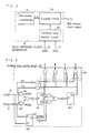
- Fig. 1 is a block diagram showing a dynamic random access memory device in one embodiment of this invention, in which a memory cell matrix 21, a row line selection circuit 22, a sense refreshing amplifier 23, and a control clock generator 25 are the same as those of the conventional circuit shown in Fig. 7, substantially.
- a refreshing address counter 26 stores the row line address to be refreshed.
- An error correction address counter 13 is synchronized with the refreshing address counter 26 and stores the column address to be corrected.
- Row line selection circuit 22 selects any one of the lines of the memory cell matrix 21 for refreshing selected memory cells, and column selection circuit 11 selects any one of the columns of the memory cell matrix for correcting selected memory cells.
- Error detection circuit 12 detects the error of the data read out from the memory cells by the self refreshing amplifier 23 and rewrites the correct data to the memory cells, and then, generates an error detection signal EDS when the error correction is executed.
- a counter circuit 14 receives a carry signal RCC from the error correction address counter 13, and is reset by the error detection signal EDS delivered from the error correction circuit 12.
- the clock period of the self-refreshing clock generator 15 is varied by the error detection signal EDS from the error correction circuit 12 or the control signal PDS from the counter circuit 14.
- Numerals 16, 17 are control signal lines of error detection signal EDS and control signal PDS.
- Fig. 2 is a block diagram showing a detailed structure of the self-refreshing clock generator 15.
- the self-refreshing clock generator 15 is composed of monostable multivibrator 31 which is self-excited, a dividing circuit 32 for dividing the output signal of the monostable multivibrator, and a dividing ratio control circuit 33 for varying the dividing ratio of the dividing circuit 32 depending on the error detection signal EDS and control signal PDS supplied from control signal lines 16, 17.
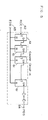
- the circuit diagram of the dividing ratio control circuit 33 is shown in Fig. 3.
- the dividing ratio control circuit 33 is composed of a binary up/down counter which is comprised of T-flip-flops 41, 45, RS-flip-flop 42 and peripheral logic circuits thereof, a decoder 43 for decoding the outputs Q1, Q2 of the T-flip-flops 41, 45 and generating output signals A, B, C, D, and two AND gates 44, 44′ for controlling signals EDSG, PDSG depending on the signals EG, PG generated based on the state of said binary up/down counter outputs Q1, Q2.
- the dividing circuit 32 is, as shown in Fig. 4, composed of four T-flip-flops 51 to 54, and five NAND gates 55 to 59.
- the input signal CLK from the monostable multivibrator shown in Fig. 2 is fed into an input terminal of the T-flip-flop 51 of the first stage, and its output Q1 is fed into an input terminal of the T-flip-flop 52 of the second stage.
- the Q2 output of the second stage T-flip-flop 52 is fed into an input terminal of the T-flip-flop 53 of the third stage.
- the NAND gate 55 receives the input signal CLK and an output signal A of the dividing ratio control circuit 33, and the NAND gates 56 to 58 respectively receive the outputs Q1 to Q3 of T-flip-flops 51 to 53, and output signals B to D of the dividing ratio control circuit 33, and the outputs of all NAND gates 55 to 58 are fed into the NAND gate 59.
- the output of the NAND gate 59 is fed into an input terminal of the T-flip-flop 54 of the final stage, and its output Q4 is supplied into the control clock generator 25 shown in Fig. 1 as a self-refreshing clock SRC.
- the circuit diagram of counter circuit 14 is shown in Fig 5.
- the counter circuit 14 is composed of a binary counter having a cascade connection of N T-flip-flops 61. Receiving a carry signal RCC coming from MSB (Most Significant Bit) of the error correction address counter shown in Fig. 1, all T-flip-flops 61 are reset by the error detection signal EDS from the error correction circuit 12 shown in Fig. 1. The QN output of the T-flip-flop 61 of the final stage is applied to the self-refreshing clock generator 15 in Fig. 1 as the control signal (counter output) PDS.
- the self-excited self-refreshing clock generator 15 generates a self-refreshing clock SRC of period T R .
- This period T R varies with the error detection signal EDS from the error correction circuit 12 and the counter output PDS from the counter circuit 14.
- self-refreshing action is done as follows.
- the memory cells corresponding to a row line specified by the refreshing address counter 26 and selected by the row line selection circuit 22 are simultaneously refreshed (read and written again) by the sense refreshing amplifier 23.
- one memory cell specified by the error correction address counter 13 and selected by the column selection circuit 11 is selected.
- Said selected memory cell is one of the memory cells corresponding to a row line selected by the row line selection circuit 22.
- the data read out from the selected memory cell is judged by the error correction circuit 12 judged if correct or wrong, and if wrong, correct data is written again, and an error detection signal EDS is generated.
- the refreshing address counter 26 is incremented, and the row line address to be refreshed is set in the next refreshing cycle.
- the memory cell matrix 21 is composed of m row lines by n columns, refreshing of all memory cells is over in m periods of said self-refreshing cycle, and correction of errors of all memory cells is over in m ⁇ n periods.
- This self-refreshing clock generator 15 includes a self-excited clock generator (the monostable multivibrator 31 in this embodiment), and the dividing ratio of the output of the monostable multivibrator can be changed from 1/2 to 1/16 depending on the error detection signal EDS and counter output PDS, so that the period may be varied according to these signals EDS, PDS.
- the dividing ratio becomes 1/2 times
- the error detection signal EDS falls
- the dividing ratio becomes 2 times.
- the minimum dividing radio does not become smaller than 1/6.
- the dividing ratio will not become more than 1/2. Therefore, if the period of the output CLK of the monostable multivibrator 31 in Fig. 2 is 100 ⁇ s, the self-refreshing clock SRC from the dividing circuit 32 is any one of 200 ⁇ s (minimum period), 400 ⁇ s, 800 ⁇ s, and 1600 ⁇ s (maximum period), and at every one fall of counter output PDS, it changes 2 times (to the maximum of 1600 ⁇ s), and every one fall of error detection signal EDS, it changes 1/2 times (to the minimum of 200 ⁇ s).
- the operation timing of the dividing ratio control circuit 33 shown in Fig. 3 is shown in Fig. 6.
- Signal EG works to prevent the fall of the error detection signal EDS from being fed into the T-flip-flop functioning as a down counter when the outputs Q1, Q2 of two T-flip-flops 41, 45 are 0 in binary notation, so that the outputs Q1, Q2 may not be inverted to 1.
- signal PG works to prevent the fall of the counter output PDS from being fed into the T-flip-flop functioning as an up counter when the outputs Q1, Q2 of T-flip-flops 41, 45 are both 1 in binary notation, so that the outputs Q1, Q2 may not be inverted to 0.
- These outputs Q1, Q2 are decoded by the decoder 43, and dividing ratio control signals A, B, C, D are obtained.
- One of these dividing ratio control signals is always 1 in binary notation, while others are 0, and the dividing ratio of the dividing circuit 32 in Fig. 4 is determined.
- signal B is binary 1
- others are binary 1
- the output Q1 of the T-flip-flop 51 is entered in the T input of the T-flip-flop 54, so that the dividing ratio is 1/4.
- signal A is binary 1
- the dividing ratio is 1/2
- D is 1, it is 1/16.
- the period T R of self-refreshing clock varies with the error detection signal EDS and counter output PDS.
- An error detection signal EDS occurs when there is an error in the data during self-refreshing cycle.
- the counter output PDS is the output of dividing the carry signal RCC coming from the MSB of the error correction address counter 13 by the counter shown in Fig. 5. Therefore, supposing the number of stages of the counter circuit 14 to be N, as far as there is no error in the data being read out in the period of m ⁇ n ⁇ 2 N , the counter output PDS rises once and falls once. Accordingly, if there is no error in the data for a period of m ⁇ n ⁇ 2 N , the period T R becomes 2 times longer.
- the self-refreshing clock period T R can be controlled by the error detection signal EDS and counter output PDS, self-refreshing can be executed in the period T R , suited to the actual value of the pause time T H of the memory cell. For example, when the ambient temperature decreases by 10°C and the pause time T H doubles, the counter output PDS is generated, and the self-refreshing period is also increased twice. In this way, if the pause time T H varies, self-refreshing action can be executed always at a value close to the maximum value of the period T R , so that the current consumption may be reduced greatly as compared with that of the conventional fixed period type.
- the dividing ratio of self-refreshing clock is set at 1/2 k (where k is 1, 2, 3, 4), but the change of the dividing ratio may be set finer by increasing the number of stages of flip-flop or extending the range of dividing ratio.
- the control signal PDS is generated by the counter circuit 14, but it may be also generated by the timer circuit which delivers a signal when error does not occur for a predetermined period.
- the clock period of self-refreshing clock is varied by using the error detection signal generated from the error correction circuit 12.
- the error correction may be made by an external error correction circuit.
- self-refreshing can be executed in a self-refreshing period close to the maximum depending on the actual pause time value even if the pause time of the memory cell varies significantly depending on the manufacturing process condition, so that the current consumption in the self-refreshing time can be decreased. Or even if the operating conditions change or the pause time of the memory cell should vary, it is possible to operate in the maximum self-refreshing period always depending on the conditions. What is more, the upper limit of the operating temperature condition can be heightened without increasing the self-refreshing current at the ordinary operating temperature.
Landscapes
- Engineering & Computer Science (AREA)
- Computer Hardware Design (AREA)
- Microelectronics & Electronic Packaging (AREA)
- Dram (AREA)
- Techniques For Improving Reliability Of Storages (AREA)
- For Increasing The Reliability Of Semiconductor Memories (AREA)
Applications Claiming Priority (2)
| Application Number | Priority Date | Filing Date | Title |
|---|---|---|---|
| JP187192/87 | 1987-07-27 | ||
| JP62187192A JPS6432489A (en) | 1987-07-27 | 1987-07-27 | Memory device |
Publications (2)
| Publication Number | Publication Date |
|---|---|
| EP0301794A1 true EP0301794A1 (de) | 1989-02-01 |
| EP0301794B1 EP0301794B1 (de) | 1991-07-10 |
Family
ID=16201713
Family Applications (1)
| Application Number | Title | Priority Date | Filing Date |
|---|---|---|---|
| EP88306838A Expired - Lifetime EP0301794B1 (de) | 1987-07-27 | 1988-07-25 | Dynamischer Speicher mit wahlfreiem Zugriff und mit Selbstauffrischungsfunktion |
Country Status (5)
| Country | Link |
|---|---|
| US (1) | US4935900A (de) |
| EP (1) | EP0301794B1 (de) |
| JP (1) | JPS6432489A (de) |
| KR (1) | KR910009440B1 (de) |
| DE (1) | DE3863604D1 (de) |
Cited By (5)
| Publication number | Priority date | Publication date | Assignee | Title |
|---|---|---|---|---|
| WO1991007756A1 (en) * | 1989-11-18 | 1991-05-30 | Active Book Company Limited | Method of refreshing memory devices |
| EP0663668A3 (de) * | 1993-09-29 | 1996-07-10 | Texas Instruments Deutschland | Verbesserungen in oder in Bezug auf EEPROMs. |
| EP0739015A3 (de) * | 1995-04-18 | 1997-04-09 | Matsushita Electric Industrial Co Ltd | Halbleiterspeicheranordnung |
| NL1000847C2 (nl) * | 1994-07-19 | 1997-05-21 | Micron Technology Inc | Progammeerbaar dynamisch willekeurig-toegankelijk geheugen (DRAM). |
| KR101046304B1 (ko) * | 2006-10-20 | 2011-07-05 | 후지쯔 가부시끼가이샤 | 메모리 장치 및 리프레시 조정 방법 |
Families Citing this family (23)
| Publication number | Priority date | Publication date | Assignee | Title |
|---|---|---|---|---|
| DE69128061T2 (de) * | 1990-08-30 | 1998-03-26 | Nippon Electric Co | Halbleiterspeicheranordnung |
| JP2856598B2 (ja) * | 1992-06-04 | 1999-02-10 | 三菱電機株式会社 | ダイナミックランダムアクセスメモリ装置 |
| JPH06124587A (ja) * | 1992-10-09 | 1994-05-06 | Mitsubishi Electric Corp | ダイナミックランダムアクセスメモリ装置 |
| US5495491A (en) * | 1993-03-05 | 1996-02-27 | Motorola, Inc. | System using a memory controller controlling an error correction means to detect and correct memory errors when and over a time interval indicated by registers in the memory controller |
| US5335202A (en) * | 1993-06-29 | 1994-08-02 | Micron Semiconductor, Inc. | Verifying dynamic memory refresh |
| US5446695A (en) * | 1994-03-22 | 1995-08-29 | International Business Machines Corporation | Memory device with programmable self-refreshing and testing methods therefore |
| WO1996028825A1 (en) * | 1995-03-15 | 1996-09-19 | Hitachi, Ltd. | Semiconductor memory |
| US6433607B2 (en) * | 1998-01-21 | 2002-08-13 | Fujitsu Limited | Input circuit and semiconductor integrated circuit having the input circuit |
| JP3177207B2 (ja) | 1998-01-27 | 2001-06-18 | インターナショナル・ビジネス・マシーンズ・コーポレ−ション | リフレッシュ間隔制御装置及び方法、並びにコンピュータ |
| JP2000048567A (ja) * | 1998-05-22 | 2000-02-18 | Mitsubishi Electric Corp | 同期型半導体記憶装置 |
| US6292869B1 (en) | 1998-08-31 | 2001-09-18 | International Business Machines Corporation | System and method for memory scrub during self timed refresh |
| JP4454083B2 (ja) | 1999-11-29 | 2010-04-21 | 株式会社ルネサステクノロジ | 半導体記憶装置 |
| JP4707803B2 (ja) * | 2000-07-10 | 2011-06-22 | エルピーダメモリ株式会社 | エラーレート判定方法と半導体集積回路装置 |
| JP2002216472A (ja) * | 2001-01-22 | 2002-08-02 | Nec Corp | 半導体記憶装置 |
| US7171605B2 (en) * | 2002-02-01 | 2007-01-30 | International Business Machines Corporation | Check bit free error correction for sleep mode data retention |
| TWI249101B (en) * | 2002-04-11 | 2006-02-11 | Via Tech Inc | Method and related apparatus for using a dynamic random access memory to substitute for a hard disk drive |
| JP4627411B2 (ja) * | 2003-05-20 | 2011-02-09 | ルネサスエレクトロニクス株式会社 | メモリ装置及びメモリのエラー訂正方法 |
| JP4608235B2 (ja) * | 2004-04-14 | 2011-01-12 | ルネサスエレクトロニクス株式会社 | 半導体記憶装置及び半導体記憶システム |
| JP4237109B2 (ja) | 2004-06-18 | 2009-03-11 | エルピーダメモリ株式会社 | 半導体記憶装置及びリフレッシュ周期制御方法 |
| US7894282B2 (en) * | 2005-11-29 | 2011-02-22 | Samsung Electronics Co., Ltd. | Dynamic random access memory device and method of determining refresh cycle thereof |
| US7975170B2 (en) * | 2007-06-15 | 2011-07-05 | Qimonda Ag | Memory refresh system and method |
| US8255740B2 (en) | 2010-09-27 | 2012-08-28 | International Business Machines Corporation | Multi-level DIMM error reduction |
| KR20170030207A (ko) * | 2015-09-09 | 2017-03-17 | 에스케이하이닉스 주식회사 | 메모리 장치 |
Citations (4)
| Publication number | Priority date | Publication date | Assignee | Title |
|---|---|---|---|---|
| EP0109069A2 (de) * | 1982-11-11 | 1984-05-23 | Kabushiki Kaisha Toshiba | Dynamische Halbleiterspeicheranordnung |
| EP0116774A2 (de) * | 1982-12-27 | 1984-08-29 | Kabushiki Kaisha Toshiba | Halbleiterspeicheranordnung mit einem Auffrischungsmechanismus |
| EP0176203A2 (de) * | 1984-08-20 | 1986-04-02 | Kabushiki Kaisha Toshiba | Automatische Refreshsteuerungsschaltung für eine dynamische Halbleiterspeicherschaltung |
| EP0212547A2 (de) * | 1985-08-16 | 1987-03-04 | Fujitsu Limited | Verfahren und Anordnung zur Auffrischung einer dynamischen Halbleiterspeicheranordnung |
Family Cites Families (7)
| Publication number | Priority date | Publication date | Assignee | Title |
|---|---|---|---|---|
| JPS5148229A (de) * | 1974-10-23 | 1976-04-24 | Hitachi Ltd | |
| JPS5250648A (en) * | 1975-10-22 | 1977-04-22 | Hitachi Ltd | Semi-conductor memory |
| JPS52137221A (en) * | 1976-05-12 | 1977-11-16 | Hitachi Ltd | Memory device |
| US4333167A (en) * | 1979-10-05 | 1982-06-01 | Texas Instruments Incorporated | Dynamic memory with on-chip refresh invisible to CPU |
| US4412314A (en) * | 1980-06-02 | 1983-10-25 | Mostek Corporation | Semiconductor memory for use in conjunction with error detection and correction circuit |
| JPS6134793A (ja) * | 1984-07-27 | 1986-02-19 | Hitachi Ltd | ダイナミツクメモリ装置における診断及びエラ−訂正装置 |
| JPS61214298A (ja) * | 1985-03-20 | 1986-09-24 | Toshiba Corp | 誤り訂正機能を備えた半導体記憶装置 |
-
1987
- 1987-07-27 JP JP62187192A patent/JPS6432489A/ja active Granted
-
1988
- 1988-07-25 DE DE8888306838T patent/DE3863604D1/de not_active Expired - Lifetime
- 1988-07-25 EP EP88306838A patent/EP0301794B1/de not_active Expired - Lifetime
- 1988-07-26 KR KR1019880009378A patent/KR910009440B1/ko not_active Expired
- 1988-07-27 US US07/225,291 patent/US4935900A/en not_active Expired - Lifetime
Patent Citations (4)
| Publication number | Priority date | Publication date | Assignee | Title |
|---|---|---|---|---|
| EP0109069A2 (de) * | 1982-11-11 | 1984-05-23 | Kabushiki Kaisha Toshiba | Dynamische Halbleiterspeicheranordnung |
| EP0116774A2 (de) * | 1982-12-27 | 1984-08-29 | Kabushiki Kaisha Toshiba | Halbleiterspeicheranordnung mit einem Auffrischungsmechanismus |
| EP0176203A2 (de) * | 1984-08-20 | 1986-04-02 | Kabushiki Kaisha Toshiba | Automatische Refreshsteuerungsschaltung für eine dynamische Halbleiterspeicherschaltung |
| EP0212547A2 (de) * | 1985-08-16 | 1987-03-04 | Fujitsu Limited | Verfahren und Anordnung zur Auffrischung einer dynamischen Halbleiterspeicheranordnung |
Cited By (7)
| Publication number | Priority date | Publication date | Assignee | Title |
|---|---|---|---|---|
| WO1991007756A1 (en) * | 1989-11-18 | 1991-05-30 | Active Book Company Limited | Method of refreshing memory devices |
| EP0663668A3 (de) * | 1993-09-29 | 1996-07-10 | Texas Instruments Deutschland | Verbesserungen in oder in Bezug auf EEPROMs. |
| NL1000847C2 (nl) * | 1994-07-19 | 1997-05-21 | Micron Technology Inc | Progammeerbaar dynamisch willekeurig-toegankelijk geheugen (DRAM). |
| EP0739015A3 (de) * | 1995-04-18 | 1997-04-09 | Matsushita Electric Industrial Co Ltd | Halbleiterspeicheranordnung |
| US5828619A (en) * | 1995-04-18 | 1998-10-27 | Matsushita Electric Industrial Co., Ltd. | Semiconductor memory device |
| KR101046304B1 (ko) * | 2006-10-20 | 2011-07-05 | 후지쯔 가부시끼가이샤 | 메모리 장치 및 리프레시 조정 방법 |
| US8539310B2 (en) | 2006-10-20 | 2013-09-17 | Fujitsu Limited | Memory device and refresh adjusting method |
Also Published As
| Publication number | Publication date |
|---|---|
| JPH0456396B2 (de) | 1992-09-08 |
| DE3863604D1 (de) | 1991-08-14 |
| KR910009440B1 (ko) | 1991-11-16 |
| JPS6432489A (en) | 1989-02-02 |
| EP0301794B1 (de) | 1991-07-10 |
| US4935900A (en) | 1990-06-19 |
| KR890002885A (ko) | 1989-04-11 |
Similar Documents
| Publication | Publication Date | Title |
|---|---|---|
| EP0301794B1 (de) | Dynamischer Speicher mit wahlfreiem Zugriff und mit Selbstauffrischungsfunktion | |
| US7701753B2 (en) | Apparatus and method for self-refreshing dynamic random access memory cells | |
| US9984738B2 (en) | Apparatuses and methods for refreshing memory cells of a semiconductor device | |
| US7013363B2 (en) | Method and circuit for adjusting a self-refresh rate to maintain dynamic data at low supply voltages | |
| KR100447563B1 (ko) | 반도체 메모리 | |
| US8547759B2 (en) | Semiconductor device performing refresh operation | |
| WO1992011638A2 (en) | Hidden refresh of a dynamic random access memory | |
| EP0109069B1 (de) | Dynamische Halbleiterspeicheranordnung | |
| KR0136448B1 (ko) | 에러 자체 정정회로를 갖는 반도체 메모리 소자 | |
| US7269085B2 (en) | Non volatile semiconductor memory device having a multi-bit cell array | |
| WO1996028825A1 (en) | Semiconductor memory | |
| US5260901A (en) | Output circuit of semiconductor memory device | |
| US10818335B2 (en) | Memory storage apparatus and operating method with multiple modes for refresh operation | |
| US6538948B2 (en) | Semiconductor device, refreshing method thereof, memory system, and electronic instrument | |
| US6738304B2 (en) | Dynamic memory device and method for controlling such a device | |
| JPH0644773A (ja) | ダイナミック型半導体メモリ | |
| US12046270B2 (en) | Memory and operation method of the same | |
| JPH0359876A (ja) | ダイナミック型半導体メモリのリフレッシュ信号生成回路 | |
| JPS62165784A (ja) | 半導体記憶装置 | |
| JPS623485A (ja) | 半導体記憶装置 |
Legal Events
| Date | Code | Title | Description |
|---|---|---|---|
| PUAI | Public reference made under article 153(3) epc to a published international application that has entered the european phase |
Free format text: ORIGINAL CODE: 0009012 |
|
| AK | Designated contracting states |
Kind code of ref document: A1 Designated state(s): DE FR GB |
|
| 17P | Request for examination filed |
Effective date: 19890224 |
|
| 17Q | First examination report despatched |
Effective date: 19901022 |
|
| GRAA | (expected) grant |
Free format text: ORIGINAL CODE: 0009210 |
|
| AK | Designated contracting states |
Kind code of ref document: B1 Designated state(s): DE FR GB |
|
| REF | Corresponds to: |
Ref document number: 3863604 Country of ref document: DE Date of ref document: 19910814 |
|
| EN | Fr: translation not filed | ||
| PLBE | No opposition filed within time limit |
Free format text: ORIGINAL CODE: 0009261 |
|
| STAA | Information on the status of an ep patent application or granted ep patent |
Free format text: STATUS: NO OPPOSITION FILED WITHIN TIME LIMIT |
|
| 26N | No opposition filed | ||
| ET | Fr: translation filed | ||
| REG | Reference to a national code |
Ref country code: FR Ref legal event code: AR |
|
| REG | Reference to a national code |
Ref country code: FR Ref legal event code: BR |
|
| PGFP | Annual fee paid to national office [announced via postgrant information from national office to epo] |
Ref country code: FR Payment date: 20010712 Year of fee payment: 14 |
|
| PGFP | Annual fee paid to national office [announced via postgrant information from national office to epo] |
Ref country code: DE Payment date: 20010716 Year of fee payment: 14 |
|
| PGFP | Annual fee paid to national office [announced via postgrant information from national office to epo] |
Ref country code: GB Payment date: 20010725 Year of fee payment: 14 |
|
| REG | Reference to a national code |
Ref country code: GB Ref legal event code: IF02 |
|
| REG | Reference to a national code |
Ref country code: GB Ref legal event code: 732E |
|
| PG25 | Lapsed in a contracting state [announced via postgrant information from national office to epo] |
Ref country code: GB Free format text: LAPSE BECAUSE OF NON-PAYMENT OF DUE FEES Effective date: 20020725 |
|
| PG25 | Lapsed in a contracting state [announced via postgrant information from national office to epo] |
Ref country code: DE Free format text: LAPSE BECAUSE OF NON-PAYMENT OF DUE FEES Effective date: 20030201 |
|
| GBPC | Gb: european patent ceased through non-payment of renewal fee |
Effective date: 20020725 |
|
| PG25 | Lapsed in a contracting state [announced via postgrant information from national office to epo] |
Ref country code: FR Free format text: LAPSE BECAUSE OF NON-PAYMENT OF DUE FEES Effective date: 20030331 |
|
| REG | Reference to a national code |
Ref country code: FR Ref legal event code: TP |
|
| REG | Reference to a national code |
Ref country code: FR Ref legal event code: ST |