EP0302178B1 - Senseur de position - Google Patents
Senseur de position Download PDFInfo
- Publication number
- EP0302178B1 EP0302178B1 EP88105743A EP88105743A EP0302178B1 EP 0302178 B1 EP0302178 B1 EP 0302178B1 EP 88105743 A EP88105743 A EP 88105743A EP 88105743 A EP88105743 A EP 88105743A EP 0302178 B1 EP0302178 B1 EP 0302178B1
- Authority
- EP
- European Patent Office
- Prior art keywords
- image
- wavelength
- point
- aberration
- magnification
- Prior art date
- Legal status (The legal status is an assumption and is not a legal conclusion. Google has not performed a legal analysis and makes no representation as to the accuracy of the status listed.)
- Expired - Lifetime
Links
- 230000004075 alteration Effects 0.000 claims description 44
- 230000003287 optical effect Effects 0.000 claims description 19
- 230000004304 visual acuity Effects 0.000 description 18
- 239000011521 glass Substances 0.000 description 10
- 239000000463 material Substances 0.000 description 10
- 210000001747 pupil Anatomy 0.000 description 6
- 201000009310 astigmatism Diseases 0.000 description 3
- 238000013461 design Methods 0.000 description 3
- 238000001514 detection method Methods 0.000 description 3
- 239000000758 substrate Substances 0.000 description 3
- 238000003384 imaging method Methods 0.000 description 2
- 238000000034 method Methods 0.000 description 2
- QNRATNLHPGXHMA-XZHTYLCXSA-N (r)-(6-ethoxyquinolin-4-yl)-[(2s,4s,5r)-5-ethyl-1-azabicyclo[2.2.2]octan-2-yl]methanol;hydrochloride Chemical compound Cl.C([C@H]([C@H](C1)CC)C2)CN1[C@@H]2[C@H](O)C1=CC=NC2=CC=C(OCC)C=C21 QNRATNLHPGXHMA-XZHTYLCXSA-N 0.000 description 1
- 238000013459 approach Methods 0.000 description 1
- 230000008094 contradictory effect Effects 0.000 description 1
- 230000007423 decrease Effects 0.000 description 1
- 238000011161 development Methods 0.000 description 1
- 230000000694 effects Effects 0.000 description 1
- 230000001678 irradiating effect Effects 0.000 description 1
- 238000012545 processing Methods 0.000 description 1
- 230000001502 supplementing effect Effects 0.000 description 1
Images




Classifications
-
- G—PHYSICS
- G03—PHOTOGRAPHY; CINEMATOGRAPHY; ANALOGOUS TECHNIQUES USING WAVES OTHER THAN OPTICAL WAVES; ELECTROGRAPHY; HOLOGRAPHY
- G03F—PHOTOMECHANICAL PRODUCTION OF TEXTURED OR PATTERNED SURFACES, e.g. FOR PRINTING, FOR PROCESSING OF SEMICONDUCTOR DEVICES; MATERIALS THEREFOR; ORIGINALS THEREFOR; APPARATUS SPECIALLY ADAPTED THEREFOR
- G03F9/00—Registration or positioning of originals, masks, frames, photographic sheets or textured or patterned surfaces, e.g. automatically
- G03F9/70—Registration or positioning of originals, masks, frames, photographic sheets or textured or patterned surfaces, e.g. automatically for microlithography
- G03F9/7003—Alignment type or strategy, e.g. leveling, global alignment
- G03F9/7023—Aligning or positioning in direction perpendicular to substrate surface
- G03F9/7026—Focusing
Definitions
- This invention relates to an apparatus having double focuses and utilizing a chromatic observation for accurately sensing the positions observed in the direction perpendicular to a common optical axis of first and second objects separated from each other by a very short distance.
- the invention relates to an apparatus for sensing the relative position, in a direction perpendicular to a common optical axis, of a first and a second object separated by a small distance along said optical axis as mentioned in the preamble of the patent claim.
- Such an apparatus is known from the DE-A-34 13 374.
- the known apparatus is used for proximity printing to optically adjust a mask on a substrate surface which mask having a small distance from the substrate.
- the structures of the mask and of the substrate are focused in a common plane using light having different wavelength.
- Such an apparatus and method can in particular be used for X-ray lithographic printing.
- the gap between the two objects must be made small in order to improve resolving power.
- the settable gap is on the order of 10 microns, resolving power must be reduced, thus making it impossible to detect the clear image necessary for highly accurate alignment.
- the first is a detecting optical system that relies upon a double focal point lens utilizing the principle of double refraction (see "X-Ray Exposure Devices" in Precision Machines , 1985, vol. 51, No. 12, pp. 34 - 38).
- the second is a detecting optical system using rhombic detection (see the specification of Japanese Patent Application Laid-Open No. 61-100930).
- the required focal depth would be 10 ⁇ m or more. Accordingly, from Eq. (1), resolving power would be less than 1.1 ⁇ m in such case.
- the alignment marks of the mask and wafer be sensed with greater clarity by raising the resolving power of the objective lens in the detecting optical system.
- the focal depth must be increased in order to set the gap between the mask and wafer to a usable range (no less than about 10 ⁇ m). It is obvious from Eqs. (1) and (2), however, that both of these requirements cannot be satisfied simultaneously.
- an object of the present invention is to provide an apparatus for sensing the positions of two spaced objects, wherein it is possible to obtain a depth of focus greater than a settable gap between the two objects upon assuring a sufficient resolving power for, e.g., highly precise alignment, while resolving power and focal depth abide by the foregoing Rayleigh equations.
- an objective lens is accompanied by other lenses such as an eyepiece and relay lens to provide an image having a certain magnification.
- other lenses such as an eyepiece and relay lens to provide an image having a certain magnification.
- the discussion will be limited solely to a single objective lens.
- a thin lens system will be dealt with and only paraxial formulae for a thin lens will be used.
- the lens position is referred to as the principal point, and this position is shown at A on the optical axis.
- the object is situated on the left side of the lens at a position M located at a distance S from the principal point. Images for the respective wavelengths can be formed at points B and C on the side of the lens opposite the object.
- the refractive index of the objective lens differs depending upon the wavelength; the shorter the wavelength, the higher the refractive index and, hence, the closer the focal point is to the lens. Accordingly, since the wavelengths are related by ⁇ ⁇ ⁇ , the image for wavelength ⁇ is formed at point B, and the image for wavelength ⁇ is formed at point C.
- S'' ⁇ , S'' ⁇ represent the distances of the respective images from the principal point.
- Fig. 2 shows the result of such movement, with the new object position being designated M'.
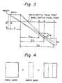
- Fig. 3 differs from Figs. 1 and 2 in that a new point D appears on the left side of point B.
- This point is that at which the image of the wafer (point M') is formed for wavelength ⁇ .
- Sd represent the distance of this point from the principal point A, we find Sd as follows: Therefore, the foregoing demonstrates that the image planes corresponding to the mask (point M) can be obtained at points B and C, and that the image planes corresponding to the wafer (point M') can be obtained at points D and B.
- the image planes for the two objects, namely the mask and the wafer will coincide at the point B in Fig. 3.
- the images at point B are in focus
- the images of the wafer and mask at the respective points D and C appear blurred due to axial spherical chromatic aberration.
- Fig. 4 Examples of the alignment marks for a mask and wafer are as shown in Fig. 4, in which the alignment marks are imagined to be rectangular and the shorter side of the mask mark is assumed to be greater than the shorter side of the wafer mark.
- Fig. 5 With the mask and wafer of Fig. 4 superimposed, the patterns which appear on the picture tube screen along with blurring caused by axial spherical chromatic aberration are illustrated in Fig. 5.
- the color associated with wavelength ⁇ is indicated by the solid lines, and the color associated with wavelength ⁇ is indicated by the broken lines.
- chromatic aberration of magnification The blurring due to chromatic aberration in Fig. 5 is referred to as chromatic aberration of magnification.
- the chromatic aberrations of magnification associated with the mask and wafer shall be denoted by Zm and Zw and are obtained by using the following equations: where h represents the length of the long side of the rectangular marks.
- the blurring expressed by Eqs. (6) and (7) is determined geometrically in Fig. 3.
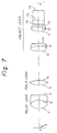
- a filter of the kind shown in Fig. 6 may be used to remove the blurred portions of Fig. 5.
- the filter illustrated in Fig. 6 is composed of two coated surfaces. One is a coated surface which passes only the light of wavelength ⁇ , while the other is a coated surface which passes only the light of wavelength ⁇ .
- the design of the filter is decided in accordance with the state of the patterns shown in Fig. 5, and the boundaries of the coated surfaces are situated intermediate those of the mask marks and wafer marks.
- Wafer-Mask Gap Wafer-Mask Gap
- a relay lens, field lens and objective lens are used in combination.
- the most important lens is the objective lens which, in the illustrated embodiment, is basically designed based on the system described in the specification of Japanese Patent Publication No. 43-15237.
- the present lens system is designed so as to employ two types of light beams, namely a g line (wavelength: 435.84 nm) and e line (wavelength: 546.07 nm).
- the Objective lens specifications are shown in Table 2.
- Fig. 8 illustrates the aberration curves. These curves also clearly show that the aberrations are well corrected.
- Table 2 Objective Lens Specifications Total optical path diameter 488.135 Focal length -1.830 Rear focal point -0.731 Front focal point 275.496 Entrance pupil 275.496 Entrance diameter 1.464 Entrance magnification -0.234 Exit pupil ***** Exit magnification ***** Object distance -1.000 Magnification (reciprocal) -0.666660D-02 Image distance 1.2202 Table 3 Data for Embodiment 1 No.
- Petzval aberration 1 0.00000 0.00000 0.00000 0.00000 0.00000 0.00000 2 -0.00020 0.00194 -0.01899 0.04884 0.47842 0.02986 3 0.00050 0.00272 0.01489 0.02383 0.13042 0.00894 4 -0.00046 -0.00490 -0.05167 -0.07318 -0.77169 -0.02151 5 0.00000 0.00009 -0.00362 -0.02475 -1.05363 -0.02113 6 0.00000 0.00008 0.00247 -0.01866 0.57849 -0.02113 7 0.00000 0.00000 0.00000 0.00000 0.00000 0.00000 0.00000 8 -0.34045 0.10352 -0.03148 -0.08289 0.02521 -0.05142 9 0.86166 0.12558 0.01830 0.03540 0.00516 -0.01710 10 -0.04013 -0.036
- the objective lens specifications are shown in Table 6.
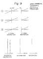
- Fig. 9 illustrates the aberration curves. These curves also show that the aberrations are well corrected.
- Table 6 Objective Lens Specifications Total optical path diameter 487.722 Focal length -1.830 Rear focal point -0.731 Front focal point 275.496 Entrance pupil 275.496 Entrance diameter 1.464 Entrance magnification -0.235 Exit pupil ***** Exit magnification ***** Object distance -1.000 Magnification (reciprocal) -0.666660D-02 Image distance 1.1917 Table 7 Data for Embodiment 2 No.
- Petzval aberration 1 0.00000 0.00000 0.00000 0.00000 0.00000 0.00000 2 -0.00020 0.00194 -0.01904 0.04889 0.47953 0.02985 3 0.00050 0.00271 0.01482 0.02376 0.12966 0.00894 4 -0.00046 -0.00489 -0.05153 -0.07304 -0.76913 -0.02151 5 0.00000 0.00009 -0.00362 -0.02475 -1.05301 -0.02113 6 0.00000 0.00008 0.00247 -0.01866 0.57858 -0.02113 7 0.00000 0.00000 0.00000 0.00000 0.00000 0.00000 0.00000 8 -0.33712 0.10348 -0.03176 -0.08317 0.02553 -0.05141 9 0.87226 0.12550 0.01806 0.03532 0.00508 -0.01727 10 -0.04319 -0.0
- the objective lens specifications are shown in Table 9.
- Fig. 10 illustrates the aberration curves. These curves also show that the aberrations are well corrected.
- Table 9 Objective Lens Specifications Total optical path diameter 488.294 Focal length -1.830 Rear focal point -0.660 Front focal point 275.503 Entrance pupil 275.503 Entrance diameter 1.464 Entrance magnification -0.234 Exit pupil ***** Exit magnification ***** Object distance -1.000 Magnification (reciprocal) -0.666660D-02 Image distance 1.2906 Table 10 Data for Embodiment 3 No.
- Petzval aberration 1 0.00000 0.00000 0.00000 0.00000 0.00000 0.00000 2 -0.00020 0.00194 -0.01897 0.04883 0.47808 0.02986 3 0.00050 0.00272 0.01492 0.02386 0.13065 0.00894 4 -0.00046 -0.00490 -0.05172 -0.07322 -0.77246 -0.02151 5 0.00000 0.00009 -0.00362 -0.02475 -1.05382 -0.02113 6 0.00000 0.00008 0.00247 -0.01866 0.57847 -0.02113 7 0.00000 0.00000 0.00000 0.00000 0.00000 0.00000 0.00000 8 -0.33667 0.10299 -0.03150 -0.08264 0.02528 -0.05113 9 0.86881 0.12554 0.01814 0.03529 0.00510 -0.01715 10 -0.03240 -0.031
Landscapes
- Physics & Mathematics (AREA)
- General Physics & Mathematics (AREA)
- Lenses (AREA)
- Exposure And Positioning Against Photoresist Photosensitive Materials (AREA)
- Automatic Focus Adjustment (AREA)
- Exposure Of Semiconductors, Excluding Electron Or Ion Beam Exposure (AREA)
- Length Measuring Devices By Optical Means (AREA)
Claims (1)
- Appareil pour détecter la position relative, dans une direction perpendiculaire à un axe optique commun, d'un premier et d'un deuxième objets séparés d'une petite distance le long dudit axe optique, comprenant :
une source de lumière disposée pour éclairer lesdits objets, au moyen d'une lumière comprenant deux longueurs d'onde α et β ;
un système de lentille (2-16) utilisant une aberration chromatique sphérique axiale dans l'axe optique pour former des images d'une marque du premier objet et d'une marque du deuxième objet, l'agencement relatif du premier objet, du deuxième objet et du système de lentille étant construit de façon que l'image de la marque du premier objet, correspondant à une longueur d'onde α, et l'image de la marque du deuxième objet, correspondant à une longueur d'onde β, soient focalisées dans un plan d'image identique (B) ;
caractérisé par des premier et deuxième éléments de filtre dont un est agencé pour supprimer sur ledit plan d'image le flou dans l'image de la première marque provoqué parl'aberration chromatique sphérique axiale pour la longueur d'onde β, et dont l'autre est agencée pour supprimer le flou dans l'image de la deuxième marque provoqué par l'aberration chromatique sphérique axiale pour la longueur d'onde α, respectivement.
Applications Claiming Priority (2)
| Application Number | Priority Date | Filing Date | Title |
|---|---|---|---|
| JP196174/87 | 1987-08-07 | ||
| JP62196174A JPS6441805A (en) | 1987-08-07 | 1987-08-07 | Position detecting apparatus of two bodies, which are separated by minute distance |
Publications (3)
| Publication Number | Publication Date |
|---|---|
| EP0302178A2 EP0302178A2 (fr) | 1989-02-08 |
| EP0302178A3 EP0302178A3 (en) | 1989-11-23 |
| EP0302178B1 true EP0302178B1 (fr) | 1994-03-16 |
Family
ID=16353429
Family Applications (1)
| Application Number | Title | Priority Date | Filing Date |
|---|---|---|---|
| EP88105743A Expired - Lifetime EP0302178B1 (fr) | 1987-08-07 | 1988-04-11 | Senseur de position |
Country Status (4)
| Country | Link |
|---|---|
| US (1) | US4918301A (fr) |
| EP (1) | EP0302178B1 (fr) |
| JP (1) | JPS6441805A (fr) |
| DE (1) | DE3888423T2 (fr) |
Families Citing this family (10)
| Publication number | Priority date | Publication date | Assignee | Title |
|---|---|---|---|---|
| EP0355496A3 (fr) * | 1988-08-15 | 1990-10-10 | Sumitomo Heavy Industries Co., Ltd. | Détecteur de position utilisant une plaque de zones fresnel sectorielle |
| JP2699282B2 (ja) * | 1989-02-27 | 1998-01-19 | 住友重機械工業株式会社 | 色収差を利用した二重焦点検出装置 |
| US5053628A (en) * | 1989-07-13 | 1991-10-01 | Matsushita Electric Industrial Co., Ltd. | Position signal producing apparatus for water alignment |
| US5114236A (en) * | 1989-08-04 | 1992-05-19 | Canon Kabushiki Kaisha | Position detection method and apparatus |
| DE68923802T2 (de) * | 1989-12-28 | 1995-12-07 | Sumitomo Heavy Industries | Verfahren zur beleuchtung mit zusammengesetzten farben sowie beleuchtung in vorgegebener wellenlänge in einem doppelfokusdetektor unter verwendung chromatischer aberration. |
| US7777870B2 (en) | 2006-12-12 | 2010-08-17 | Evident Technologies, Inc. | Method and system for the recognition of an optical signal |
| US7804587B2 (en) * | 2006-12-12 | 2010-09-28 | Evident Technologies, Inc. | System for the recognition of an optical signal and materials for use in such a system |
| US8879058B2 (en) * | 2010-11-05 | 2014-11-04 | The University Of Ottawa | Miniaturized multimodal cars endoscope |
| JP2012216728A (ja) * | 2011-04-01 | 2012-11-08 | V Technology Co Ltd | 露光装置のアライメント装置 |
| JP5747306B2 (ja) * | 2011-05-23 | 2015-07-15 | 株式会社ブイ・テクノロジー | 露光装置のアライメント装置 |
Family Cites Families (8)
| Publication number | Priority date | Publication date | Assignee | Title |
|---|---|---|---|---|
| JPS5635066B2 (fr) * | 1973-09-06 | 1981-08-14 | ||
| US3990798A (en) * | 1975-03-07 | 1976-11-09 | Bell Telephone Laboratories, Incorporated | Method and apparatus for aligning mask and wafer |
| JPS6042725A (ja) * | 1983-08-18 | 1985-03-07 | Olympus Optical Co Ltd | 焦点検出装置 |
| US4650983A (en) * | 1983-11-07 | 1987-03-17 | Nippon Kogaku K. K. | Focusing apparatus for projection optical system |
| DE3413374A1 (de) * | 1984-04-10 | 1985-10-17 | Licentia Patent-Verwaltungs-Gmbh, 6000 Frankfurt | Optisches justierverfahren |
| US4734570A (en) * | 1985-11-20 | 1988-03-29 | Olympus Optical Co., Ltd. | Active focus detecting device with infrared source |
| JP2614843B2 (ja) * | 1985-12-02 | 1997-05-28 | オリンパス光学工業株式会社 | 自動焦点顕微鏡 |
| JP2797250B2 (ja) * | 1987-05-14 | 1998-09-17 | 株式会社ニコン | 投影露光装置 |
-
1987
- 1987-08-07 JP JP62196174A patent/JPS6441805A/ja active Granted
-
1988
- 1988-04-11 DE DE3888423T patent/DE3888423T2/de not_active Expired - Fee Related
- 1988-04-11 EP EP88105743A patent/EP0302178B1/fr not_active Expired - Lifetime
-
1989
- 1989-04-27 US US07/344,247 patent/US4918301A/en not_active Expired - Lifetime
Also Published As
| Publication number | Publication date |
|---|---|
| EP0302178A3 (en) | 1989-11-23 |
| US4918301A (en) | 1990-04-17 |
| JPS6441805A (en) | 1989-02-14 |
| JPH054601B2 (fr) | 1993-01-20 |
| EP0302178A2 (fr) | 1989-02-08 |
| DE3888423D1 (de) | 1994-04-21 |
| DE3888423T2 (de) | 1994-10-27 |
Similar Documents
| Publication | Publication Date | Title |
|---|---|---|
| US5999310A (en) | Ultra-broadband UV microscope imaging system with wide range zoom capability | |
| CA1046823A (fr) | Microscope a double mise au point pour reperage de masques et de pastilles de semiconducteurs | |
| GB1559666A (en) | Unit magnification optical system | |
| US5137363A (en) | Projection exposure apparatus | |
| EP0302178B1 (fr) | Senseur de position | |
| EP1261890B1 (fr) | Lentille amelioree d'inspection microscopique | |
| JPH04261545A (ja) | 色収差2重焦点装置における帯域光および複色光照明方法 | |
| EP0416651B1 (fr) | Système de lentilles apochromatiques | |
| KR101130594B1 (ko) | 애퍼크로매틱 단위 배율 투영 광학 시스템 | |
| JPH0731300B2 (ja) | 焦点検出装置 | |
| KR101109844B1 (ko) | 프로젝션 광학 시스템 | |
| US4712886A (en) | Lens doublet color-corrected for visible and near-infrared wavelengths | |
| JPS6229770B2 (fr) | ||
| US7957069B2 (en) | Projection optical system | |
| US5815747A (en) | Camera having autofocus function independent of photographing optical system | |
| US20060007554A1 (en) | Method and apparatus for maintaining focus and magnification of a projected image | |
| US4898457A (en) | Optical system of television camera | |
| JPS6257008B2 (fr) | ||
| JP2000155267A (ja) | 顕微鏡対物レンズ | |
| US12529876B2 (en) | Compact optical microscope, metrology device comprising the optical microscope and a wafer positioning metrology apparatus comprising the metrology device | |
| US4723846A (en) | Optical path length compensating optical system in an alignment apparatus | |
| JPS62293718A (ja) | 露光装置 | |
| US4939357A (en) | Optical system for a focal point detecting device | |
| JP2649391B2 (ja) | 色収差を利用した2重焦点検出装置における複色照明方法および帯域光照明方法 | |
| US20240369946A1 (en) | Optical system for a metrology system and metrology system with such an optical system |
Legal Events
| Date | Code | Title | Description |
|---|---|---|---|
| PUAI | Public reference made under article 153(3) epc to a published international application that has entered the european phase |
Free format text: ORIGINAL CODE: 0009012 |
|
| AK | Designated contracting states |
Kind code of ref document: A2 Designated state(s): DE FR GB NL |
|
| PUAL | Search report despatched |
Free format text: ORIGINAL CODE: 0009013 |
|
| AK | Designated contracting states |
Kind code of ref document: A3 Designated state(s): DE FR GB NL |
|
| 17P | Request for examination filed |
Effective date: 19900126 |
|
| 17Q | First examination report despatched |
Effective date: 19920917 |
|
| GRAA | (expected) grant |
Free format text: ORIGINAL CODE: 0009210 |
|
| AK | Designated contracting states |
Kind code of ref document: B1 Designated state(s): DE FR GB NL |
|
| REF | Corresponds to: |
Ref document number: 3888423 Country of ref document: DE Date of ref document: 19940421 |
|
| ET | Fr: translation filed | ||
| PLBE | No opposition filed within time limit |
Free format text: ORIGINAL CODE: 0009261 |
|
| STAA | Information on the status of an ep patent application or granted ep patent |
Free format text: STATUS: NO OPPOSITION FILED WITHIN TIME LIMIT |
|
| 26N | No opposition filed | ||
| PGFP | Annual fee paid to national office [announced via postgrant information from national office to epo] |
Ref country code: GB Payment date: 19970325 Year of fee payment: 10 |
|
| PGFP | Annual fee paid to national office [announced via postgrant information from national office to epo] |
Ref country code: FR Payment date: 19970423 Year of fee payment: 10 |
|
| PGFP | Annual fee paid to national office [announced via postgrant information from national office to epo] |
Ref country code: NL Payment date: 19970428 Year of fee payment: 10 |
|
| PG25 | Lapsed in a contracting state [announced via postgrant information from national office to epo] |
Ref country code: GB Free format text: LAPSE BECAUSE OF NON-PAYMENT OF DUE FEES Effective date: 19980411 |
|
| PG25 | Lapsed in a contracting state [announced via postgrant information from national office to epo] |
Ref country code: FR Free format text: THE PATENT HAS BEEN ANNULLED BY A DECISION OF A NATIONAL AUTHORITY Effective date: 19980430 |
|
| PG25 | Lapsed in a contracting state [announced via postgrant information from national office to epo] |
Ref country code: NL Free format text: LAPSE BECAUSE OF NON-PAYMENT OF DUE FEES Effective date: 19981101 |
|
| GBPC | Gb: european patent ceased through non-payment of renewal fee |
Effective date: 19980411 |
|
| NLV4 | Nl: lapsed or anulled due to non-payment of the annual fee |
Effective date: 19981101 |
|
| REG | Reference to a national code |
Ref country code: FR Ref legal event code: ST |
|
| PGFP | Annual fee paid to national office [announced via postgrant information from national office to epo] |
Ref country code: DE Payment date: 20050407 Year of fee payment: 18 |
|
| PG25 | Lapsed in a contracting state [announced via postgrant information from national office to epo] |
Ref country code: DE Free format text: LAPSE BECAUSE OF NON-PAYMENT OF DUE FEES Effective date: 20061101 |