EP0302511B1 - Folgedekoder mit kurzem Resynchronisationsintervall - Google Patents
Folgedekoder mit kurzem Resynchronisationsintervall Download PDFInfo
- Publication number
- EP0302511B1 EP0302511B1 EP19880112785 EP88112785A EP0302511B1 EP 0302511 B1 EP0302511 B1 EP 0302511B1 EP 19880112785 EP19880112785 EP 19880112785 EP 88112785 A EP88112785 A EP 88112785A EP 0302511 B1 EP0302511 B1 EP 0302511B1
- Authority
- EP
- European Patent Office
- Prior art keywords
- address
- symbols
- decoder
- buffer storage
- storage means
- Prior art date
- Legal status (The legal status is an assumption and is not a legal conclusion. Google has not performed a legal analysis and makes no representation as to the accuracy of the status listed.)
- Expired - Lifetime
Links
- 239000000872 buffer Substances 0.000 claims description 47
- 230000004044 response Effects 0.000 claims description 18
- 230000005540 biological transmission Effects 0.000 claims description 11
- 238000001514 detection method Methods 0.000 claims description 9
- 230000010363 phase shift Effects 0.000 claims description 7
- 238000000034 method Methods 0.000 description 9
- 238000010586 diagram Methods 0.000 description 4
- 230000015654 memory Effects 0.000 description 4
- 230000006870 function Effects 0.000 description 3
- 101100041125 Arabidopsis thaliana RST1 gene Proteins 0.000 description 2
- 101100443250 Saccharomyces cerevisiae (strain ATCC 204508 / S288c) DIG1 gene Proteins 0.000 description 2
- 101100443251 Saccharomyces cerevisiae (strain ATCC 204508 / S288c) DIG2 gene Proteins 0.000 description 2
- 101100041128 Schizosaccharomyces pombe (strain 972 / ATCC 24843) rst2 gene Proteins 0.000 description 2
- 238000006243 chemical reaction Methods 0.000 description 2
- 230000001186 cumulative effect Effects 0.000 description 2
- 230000002457 bidirectional effect Effects 0.000 description 1
- 230000004048 modification Effects 0.000 description 1
- 238000012986 modification Methods 0.000 description 1
- 238000010587 phase diagram Methods 0.000 description 1
- 238000011084 recovery Methods 0.000 description 1
Images


Classifications
-
- H—ELECTRICITY
- H03—ELECTRONIC CIRCUITRY
- H03M—CODING; DECODING; CODE CONVERSION IN GENERAL
- H03M13/00—Coding, decoding or code conversion, for error detection or error correction; Coding theory basic assumptions; Coding bounds; Error probability evaluation methods; Channel models; Simulation or testing of codes
- H03M13/37—Decoding methods or techniques, not specific to the particular type of coding provided for in groups H03M13/03 - H03M13/35
- H03M13/39—Sequence estimation, i.e. using statistical methods for the reconstruction of the original codes
-
- H—ELECTRICITY
- H03—ELECTRONIC CIRCUITRY
- H03M—CODING; DECODING; CODE CONVERSION IN GENERAL
- H03M13/00—Coding, decoding or code conversion, for error detection or error correction; Coding theory basic assumptions; Coding bounds; Error probability evaluation methods; Channel models; Simulation or testing of codes
- H03M13/33—Synchronisation based on error coding or decoding
-
- H—ELECTRICITY
- H04—ELECTRIC COMMUNICATION TECHNIQUE
- H04L—TRANSMISSION OF DIGITAL INFORMATION, e.g. TELEGRAPHIC COMMUNICATION
- H04L27/00—Modulated-carrier systems
- H04L27/32—Carrier systems characterised by combinations of two or more of the types covered by groups H04L27/02, H04L27/10, H04L27/18 or H04L27/26
- H04L27/34—Amplitude- and phase-modulated carrier systems, e.g. quadrature-amplitude modulated carrier systems
- H04L27/38—Demodulator circuits; Receiver circuits
- H04L27/3845—Demodulator circuits; Receiver circuits using non - coherent demodulation, i.e. not using a phase synchronous carrier
- H04L27/3854—Demodulator circuits; Receiver circuits using non - coherent demodulation, i.e. not using a phase synchronous carrier using a non - coherent carrier, including systems with baseband correction for phase or frequency offset
- H04L27/3872—Compensation for phase rotation in the demodulated signal
Definitions
- the present invention relates generally to a sequential decoder for decoding convolutional codes.
- the current practice involves segmenting data to be transmitted into several information symbols and converting them into convolutionally coded symbols using a forward error correction encoder and decoding transmitted symbols by an error correction decoder according to an algorithm which is known as the Fano algorithm.
- the error correction encoder is provided with a state holding circuit and a function generator.
- the state holding circuit is typically composed of a shift register which retains its internal state but changes its state when it receives an information symbol.
- the function generator receives the internal state of the shift register to generate a coded symbol.
- the signal received by the decoder for hard-decision decoding does not necessarily match what is actually transmitted due to lost or corruption of data bits during transmission or due to indefiniteness present in the amplitude levels of demodulated QAM or PSK signals resulting from phase errors introduced to the recovered carrier.
- the decoder can be said to have the same circuit function as the error correction encoder, or a "replica of the encoder".
- the decoder compares it with each of information symbols which can be obtained by the replica of the encoder if it were to receive all possible information symbols and assumes an information symbol that is nearest to the received symbol as transmitted,
- the yardstick for measuring the distance to the nearest coded symbol is the Fano likelihood which is currently employed. According to the Fano algorithm, an information symbol sequence which gives the largest cumulative value is assumed to be the most likely message sequence.
- the decoder If a large number of transmission errors should occur, there is a possibility that the decoder makes a false decision. After having taking a wrong decision, the discrepancies between the internal states of the encoder replica and those in the encoder grow much more rapidly than would be the case if the decoder were following the correct path, and all subsequent attempts would fail to find symbols having a large Fano likelihood value, thus making it possible to detect that a false decision has been made in the past. On detecting a false decision, the decoder retraces its path to return the internal states of the encoder replica to a point where the false decision was made and takes an alternate path that gives the next largest cumulative value of the Fano likelihood and performs a decoding step on the selected path.
- the decoder If the decoder should fall in the search, it retraces further back to a past state to repeat the process. In this way, the decoder attempts to search for a correct path on the basis of trial and error. Since the past histories are retraced in the sequential decoder, the input and output symbols are stored in buffers.
- error correction encoder and decoder mentioned above can be implemented by a circuit shown and described in United States Patent 3,665,396 issued to George David Forney, Jr.
- the decoder In order to achieve the comparison between the output symbols of the encoder replica and the input symbols to that replica, the decoder must be able to detect the starting and ending points of each coded symbol on which the comparison is performed. Stated otherwise, the comparison should be performed in synchronism with each received coded symbol. Since the received symbol does not usually contain timing information, such as sync codes, the prior art sequential decoder performs the following code resynchronization process on a trial and error basis.
- the decoding process Since out-of-sync conditions can result in a situation which is equivalent to the occurrence of a serious transmission error, the decoding process encounters a substantially delay, tending to overflow the buffers. Such overflow conditions can therefore be taken as an indication of the occurrence of an out-of-sync condition
- the decoder On detecting a buffer overflow, the decoder shifts the sync timing by one symbol bit before proceeding to decode on a trial basis a fresh symbol entered next into the input buffer. If this trial attempt still does not work to alleviate the overflow, the same process is repeated. Assume that each coded symbol is made up of n coded bits, there are n possible states which can be retraced to reestablish synchronism.
- a maximum of ( n -1) trial attempts eventually enables the decoder to reestablish synchronism. If the decoder should fall in advancing its decoding process further possibly due to out-of-sync, a single trial attempt for resynchronization will require the input buffer to store a maximum number of symbols that can be stored therein. The maximum amount of time taken to resynchronize the decoder is therefore ( n -1) times the interval taken to store the maximum number of symbols into the input buffer. In addition, whole symbols stored in the input buffer must be discarded wherever a resynchronization is attempted.
- US-A-4,539,684 relates to a digital communications system using a convolutional encoding and decoding technique to minimize transmission time and decoding time.
- An autosynchronization sequence stored in a first memory is modulo-2 summed with a convolutional code sequence by an adder and presented to a bit interleaver which scrambles the information and parity bits to add time diversity so that relatively short burst errors may be corrected at the receiver.
- the transmitted data is selected by a selector with the best phase, bit-deinterleaved and modulo-2 summed with an autosynchronization sequence stored in a second memory to remove the transmitted autosynchronization sequence if the correct phase is selected.
- a modified sequential decoder controls the selector, bit-deinterleaver and memory to select the best phase.
- the resynchronization attempt of the prior art sequential decoder can therefore take as long as ( n -1) times the length of whole storage time of the input buffer. Therefore, no input data can be received during that interval.
- the sequential decoder of the present invention particularly comprises first and second buffers, or random access memories, and a decoder coupled to the first and second buffers for decoding a symbol bidirectionally supplied from the buffers in synchronism with a clock pulse occurring at a rate higher than the transmission rate of the symbol.
- An address circuit is connected to the first and second buffers for writing the received convolutionally coded symbols into the first buffer at the transmission rate, reading symbols out of the first buffer storage means into the decoder and writing symbols decoded by the decoder into the second buffer.
- a controller determines the likelihood of each symbol decoded by the decoder in accordance with a predetermined likelihood algorithm to cause the address circuit to read decoded symbols in a backward direction out of the second buffer into the decoder when the determination results in a low likelihood value.
- the controller detects an overflow condition of the first buffer when a first predetermined number M1 of locations of the first buffer are filled with received symbols.
- the controller In response to the detection of the overflow condition, the controller causes the address circuit to read symbols out of the first buffer into the decoder starting with a symbol spaced by M1-M2 symbols form a most recently received symbol and causes the decoder to repeatedly perform decoding, upon detection of the overflow condition, on a symbol which is shifted by one clock interval, where M2 is a second predetermined number which is smaller than the first predetermined number M1.
- the first predetermined number represents the capacity or maximum number of locations of each buffer.
- an out-of-sync condition can be detected by the detection of the buffer overflow.
- a phase error introduced to a recovered carrier can be compensated for by a phase switching circuit which varies the logic level of the received symbols by an amount corresponding to a predetermined phase shift immediately following the detection of the buffer overflow.
- the address circuit comprises a first address counter for incrementing a first address count in response to receipt of each of the convolutionally coded symbols and storing each of the received coded symbols into the first buffer storage means in accordance with the first address count; and a second address counter for reading symbols out of the first buffer storage means in accordance with a second address count.
- the second address count is incremented by the control circuit when the determination of the decoding algorithm results in a high likelihood value and decremented when the determination results in a low likelihood value.
- the second address count is further incremented by an amount equal to the second predetermined number when the buffer overflow is detected.
- the second address count is reset so that it equals the first address count when the buffer overflow is detected.
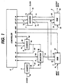
- a sequential decoder according to an embodiment of the present invention.
- Convolutional codes are modulated upon a carrier and transmitted from a transmit end of a link and received by a demodulator, not shown, at a receive end of the link.
- the received signal is demodulated to recover the convolutional code symbols.
- a clock recovery circuit not shown, recovers clock pulses from the demodulated convolutional codes and feeds them into the input terminal 3a of an "M1-bit" address counter 3 for generating an address signal A1.
- Address signal A1 is supplied from the output terminal 3b of counter 3 to terminal A1 of a controller 6 and to input terminal 5a of an address selector 5.
- Selector 5 has a second input terminal 5b to which an address signal A2 from the output terminal 4a of another "M1-bit" address counter 4 is also applied.
- Selector 5 is responsive to a switching control signal supplied from a terminal SEL of the controller 6 to selectively couple the input address signals A1 and A2 to its output terminal 5c which is connected to address terminals 1c and 2c of RAMs 1 and 2.
- RAMs 1 and 2 serve as input and output buffers each having "M1" symbol (or bit) storage locations.
- the received data bit is fed to an input terminal 1a of RAM 1 and written into a storage location specified by the address signal A1 and read out of the RAM 1 in response to the address signal A2 from counter 4.
- Data bits stored in RAM 1 are sequentially read out of the locations which are specified by the address signal A2 and fed into a decoder 7 through output terminal 1b and input terminal 7a.
- the address signal A2 thus represents the location of a symbol in RAM 1 on which decoding is in progress.
- Address counter 4 starts incrementing its count from a zero count value in response to a signal received at terminal 4b from UP terminal of the controller 6 and decrements the count in response to a signal received at terminal 4c from DW terminal of the controller 6 and supplies its output to terminal A2 of the controller 6 as well as to the second input 5b of selector 5.
- address counter 4 is reset by a signal received at terminal 4d from RST terminal of the controller 6 to reset its initial value to M2 which is smaller than M1 whenever an overflow condition of RAM 1 is detected by controller 6.
- the decoder 7 essentially comprises a bidirectional shift register and a plurality of exclusive-OR modulo-2 summers connected to some of the shift register stages in a configuration known as a "replica of the convolutional encoder".
- the shift register of the decoder 7 is normally shifted forward in response to the completion of a decoding operation on a coded symbol from RAM 1. Decoded symbols sequentially appear at an output terminal 7b and are fed through an input terminal 2a to RAM 2 and sequentially read therefrom and supplied to an external circuit, not shown, through output terminal 2b as output data if no data error occurs in the input data stream.
- the shift register is shifted backward when decoding is to be repeated on symbols.
- Decoder 7 receives a clock pulse through terminal 7d. This clock pulse occurs at a rate much higher than the rate of the clock pulse supplied to the counter 3.
- two input signals are supplied from terminal 7e to terminal IN of the controller 6. One of these signals represents a decoded symbol and the other the corresponding nondecoded symbol. These signals are compared with each other using the Fano algorithm to determine the Fano likelihood value and hence the distance to the most likelihood path.
- Decoder 7 is constructed to receive shift and stop command signals respectively at terminals 7f and 7g from terminals SFT and STP of the controller 6 in accordance with the decision of the controller 6 made in accordance with the Fano algorithm.
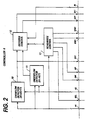
- the controller 6 essentially comprises an overflow detector 10 which detects when RAM 1 is overflowed and supplies the reset signal mentioned above to the address counter 4. This overflow condition is given when the address count A1 becomes equal to the count A2 minus 1.
- An underflow detector 11 is provided to detect when RAM 1 is underflowed. The underflow condition exists when the address count A1 becomes equal to the count A2.
- a decoder controller 12, which implements the Fano algorithm, is arranged to receive signals from the detectors 10 and 11 and signals from the decoder 7 and supplies decoder control signals including forward/backward shift command signals and a stop command signal.
- a read/write controller 13 is associated with the decoder controller 12 and the counter 3 to supply read/write control signals including the repeat command signal to RAM 2, switching signal to selector 5, up/down count signals to counter 4 to increment or decrement the address count A2 and read/write enable signals to RAMs 1 and 2.
- the address counter 3 In response to the receipt of a fresh symbol, the address counter 3 is Incremented by the corresponding clock pulse, producing an address signal A1 which is applied through selector 5 to RAMs 1 and 2 to write the received fresh symbol into a storage location specified by the address signal A1 and read out a decoded symbol out of the random access memory 2 from a storage location specified by the address signal A1 for delivery to an external circuit.
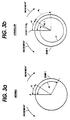
- the address signal A2 will be incremented to such a point approaching the address signal A1 if there is no transmission error (see Fig. 3a).
- the decoder 7 is in readiness to instantly perform a decoding operation on each fresh symbol as soon as it is received and stored into RAM 1. If this normal condition continues, no symbols will eventually be left in RAM 1 to be decoded.
- This underflow condition of RAM 1 is detected by the underflow detector 11. When the address counts A1 and A2 become equal to each other, underflow detector 11 communicates this fact to the decoder controller 12 to cause it to supply a stop command signal through terminal STP to the decoder 7.
- the decoder controller 12 supplies a backward shift command signal through terminal SFT to the decoder 7 to cause it to shift backward to retrace the path of the code tree.
- the read/write controller 13 decrements the address counter 4 by one through terminal DW and switches RAM 2 to a read mode to read out previously decoded symbols.
- the overflow detector 10 When the address count A1 becomes equal to the count A2 minus 1 (which corresponds to a situation in which there is a difference of only one node in the code tree between the symbol just read out of RAM 1 into the decoder 7 and a fresh symbol just written into RAM 1), the overflow detector 10 generates a reset signal through terminal RST to reset the initialized value of the address counter 4 to M2 which is smaller than the maximum address count M1. As a result, the address count A1 is rapidly incremented by M2.
- the decoder controller 12 supplies a backward shift command through terminal SFT to decoder 7 to shift the timing of the decoder 7 by one coded symbol. In this way, the decoding process restarts with a symbol which is written into RAM 1 by M2 symbols older than the most recently written symbol. If this resetting operation fails and an overflow condition occurs again in RAM 1, the process is repeated. Since no decoding operation proceeds during the time interval between the time at which the counter 4 is reset and the time at which the overflow condition occurs again and such time interval is equal to (M1 - M2) times the interval between successive clock pulses. If each coded symbol is composed of N bits, synchronization can be reestablished by repeating the one-bit shifting of the coded symbol by (N-1) times at most as will be understood from the description given above.
- this time interval is reduced to (M1 - M2) in the present invention, thus the maximum amount of time taken by the sequential decoder of the invention to resynchronize is reduced by a factor (M1 - M2)/M1 . Therefore, the number of symbols which must be discarded during a resynchronization can be reduced to M1 - M2 - 1 .
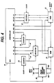
- FIG. 4 A modified embodiment of the present invention is shown in Fig. 4.
- 4-bit/symbol convolutional codes are transmitted on a 16QAM (quadrature amplitude modulation) system having a code rate 3/4.
- Received modulated codes are demodulated by a 16-QAM demodulator into a pair of in-phase (P-channel) and out-of-phase (Q-channel) signals each having one of four different amplitude levels which correspond respectively to the four phases on each axis of the phase diagram.
- Each of these signals is converted to a two-bit signal by comparison with hard-decision thresholds in a well known manner by means of an analog-to-digital converter, not shown.
- the two-bit I and Q signals which comprise a symbol, are supplied as Dp1 and Dq1 to a phase switching circuit 28.
- Phase switching circuit 28 converts the logic states of the input two-bit signals so that it compensates for phase errors introduced to the reference carrier recovered by the demodulator.
- the conversion of one logic state to another is a quantum step corresponding to a phase shift of 90 degrees.
- successive logic state conversions result in phase shifts of 180 and 270 degrees.
- the two-bit outputs of the phase switching circuit 28 are combined into a 4-bit output and fed to a RAM 21 for storing a maximum of N 4-bit symbols.
- Each 4-bit symbol is written into a storage location of RAM 1 specified by an address signal A1 supplied from an N-bit address counter 23 through a selector 25.
- the address counter 23 is incremented in response to each of the recovered clock pulses.
- Stored 4-bit symbols are read out of RAM 21 into a decoder 27 in response to an address signal A2 supplied from an N-bit address counter 24 which is incremented or decremented by a signal from a controller 26.
- controller 26 receives a signal through terminal A1 to cause the selector 25 to switch its output to the input from counter 23 in response to each increment of the address count A1 and switches RAM 21 through read/write enable terminal R/W1 to a write mode to store a fresh symbol into the location specified by count A1 and switches RAM 22 to a read mode through read/write enable terminal R/W2 to read out a stored decoded symbol from a location specified by the address count A1 for delivery to an external circuit.
- decoder 27 supplies signals to controller 26 to cause it to switch RAM 21 to a read mode and RAM 22 to a write mode and switches the selector 25 to supply address count A2 to the RAMs 21 and 22, whereby the decoded symbol is written into RAM 22. Address count A2 is then incremented to read the next symbol from RAM 21 into the decoder 27. Whenever there is a high likelihood of an error, the counter 24 is decremented through terminal DW by controller 26 to repeat the decoding operation on previously decoded symbols.
- the controller 26 is generally similar to the controller 6 of Fig. 2 with the exception that it further includes a suboverflow detector 30B in addition to the overflow detector 30A which is identical to overflow detector 10 of Fig. 2. Elements 31, 32 and 33 correspond respectively to elements 11, 12 and 13 of Fig. 2.
- Overflow detector 30A detects when the address signal A1 is equal to address count A2 minus 1 to supply a first reset signal through reset terminal RST1 to the phase switching circuit 28 and a second reset signal to the address counter 24 through reset terminal RST2.
- the first reset signal causes the phase switching circuit 28 to switch the logic states of the binary quadrature signals so that the converted logic states correspond to a phase which is shifted by a predetermined amount with respect to the phase of the input signals.
- the second reset signal is to reset the address count value A2 equal to the address count A1.
- Overflow detector 30A further supplies an enable signal to the suboverflow detector 30B when it detects an overflow condition in RAM 21.
- Suboverflow detector 30B is rendered active in response to the enable signal from overflow detector 30A to detect if a "suboverflow" condition occurs in RAM 21, i.e., RAM 21 is filled with symbols smaller than its capacity. This "suboverflow" condition occurs when the address count A1 becomes equal to A2 + N1 (where N1 is typically 1/10 of the number of the address locations N of RAM 21).
- Suboverflow detector 30B generates the first and second reset signals in a manner identical to those generated by the overflow detector 30A. Decoder controller 32 responds to the second reset signals from detectors 30A and 30B to initiate counting symbols which have been decoded by decoder 27 and disables the suboverflow detector 30B when the count reaches N2 which is much smaller than N.
- the address count A1 becomes equal to A2 - 1 and the overflow detector 30A of controller 26 detects this condition and supplies a first reset signal through terminal RST1 to the phase switching circuit 28.
- the logic state of one or both of the incoming two-bit signals Dp1 and Dq1 is converted so that the 4-bit output symbol is advanced by 90 degrees with respect to the incoming symbol.
- the reset logic states are maintained until they are reset again.
- a second reset signal is supplied from the overflow detector 30A through terminal RST2 to the address counter 24 to reset its count equal to the address count A1 of counter 23 (Fig. 6a).
- a shift command signal is applied to the decoder 27 through terminal SFT to shift the sync timing by one clock interval. If these resetting operations is not effective in completely compensating for the phase error, RAM 21 will be again filled with a growing number of unprocessed symbols. Since the suboverflow detector 30B is enabled by the overflow detector 30A, a "suboverflow" condition will be detected when A1 becomes equal to A2 + N1 (see Fig. 6b). The phase switching circuit 28 is set to introduce another 90 degree phase shift to the incoming digital signals, giving a phase shift with a total of 180 degrees and the address counter 24 is again reset equal to A1.
Landscapes
- Engineering & Computer Science (AREA)
- Physics & Mathematics (AREA)
- Probability & Statistics with Applications (AREA)
- Theoretical Computer Science (AREA)
- Computer Networks & Wireless Communication (AREA)
- Signal Processing (AREA)
- Error Detection And Correction (AREA)
Claims (5)
- Ein Folgedecoder zur Decodierung von konvolutionell codierten Symbolen, die mit einer Übertragungsrate der Symbole empfangen werden, der eine erste und eine zweite Pufferspeichereinrichtung (1, 2; 21, 22), einen Decoder (7; 27), der mit der ersten und der zweiten Pufferspeichereinrichtung (1, 2; 21, 22) zum Empfang eines Symbols verbunden ist, das bidirektional von der ersten und der zweiten Pufferspeichereinrichtung zugeführt wird, und zur Decodierung des zugeführten Symbols synchron mit einem Taktimpuls, der mit einer Rate höher als die Übertragungsrate auftritt, Adressiereinrichtungen (3, 4, 5; 23, 24, 25) zur Speicherung der empfangenen konvolutionell codierten Symbole in der ersten Pufferspeichereinrichtung (1; 21) mit der Übertragungsrate, wobei Symbole aus der ersten Pufferspeichereinrichtung (1; 21) in den Decoder (7; 27) ausgelesen werden und die durch den Decoder (7; 27) decodierten Symbole in der zweiten Pufferspeichereinrichtung (2; 22) gespeichert werden, und eine Steuereinrichtung (6; 26) zur Ermittlung der Wahrscheinlichkeit jedes Symbols aufweist, das durch den Decoder (7; 27) decodiert wird, und zwar in Abhängigkeit eines vorgegebenen Wahrscheinlichkeits-Algorithmus, der bewirkt, daß die Adressiereinrichtungen (3, 4, 5; 23, 24, 25) decodierte Symbole in einer Rückwärtsrichtung aus der zweiten Pufferspeichereinrichtung (2; 22) in den Decoder (7; 27) einlesen, wenn die Ermittlungsergebnisse zu einem niedrigen Wahrscheinlichkeitswert führen, und wobei ein Überlaufzustand der ersten Pufferspeichereinrichtung (1; 21) ermittelt wird, wenn eine erste vorgegebene Zahl M1 von Stellen davon mit den empfangenen Symbolen aufgefüllt sind, gekennzeichnet dadurch, daß die Steuereinrichtung (6; 26) Einrichtungen (10, 11, 13; 30, 31, 33) aufweist, um zu bewirken, daß die Adressiereinrichtungen (3, 4, 5; 23, 24, 25) Symbole aus der ersten Pufferspeichereinrichtung (1; 21) zu dem Decoder hin auslesen, wobei mit einem Symbol gestartet wird, das um M1-M2 Symbole von einem am kürzesten vorher empfangenen Symbol beabstandet ist, und das Einrichtungen (12; 22) zum Bewirken, daß der Decoder (7; 27) wiederholt das Decodieren durchführt, aufweist, und zwar unter Ermittlung eines Überlaufzustands, und zwar auf einem Symbol, das um ein Taktintervall verschoben ist, wobei M2 eine zweite vorgegebene Zahl ist, die kleiner als die erste vorgegebene Zahl M1 ist.
- Folgedecoder nach Anspruch 1, dadurch gekennzeichnet, daß die Adressiereinrichtungen einen ersten Adressenzähler (3) zum Erhöhen eines ersten Adressenzählwerts in Abhängigkeit des Empfangs jedes der konvolutionell codierten Symbole aufweist, und wobei jeder der empfangenen codierten Symbole in der ersten Pufferspeichereinrichtung (1) entsprechend dem ersten Adressenzählwert gespeichert wird, und einen zweiten Adressenzähler (4) zum Variieren eines zweiten Adressenzählwerts in Abhängigkeit eines Steuersignals von der Steuereinrichtung (6) aufweist, und wobei Symbole der ersten Pufferspeichereinrichtung (1) entsprechend dem zweiten Adressenzählwert ausgelesen werden, und daß die Steuereinrichtung Einrichtungen (10, 12, 13) zum Erzeugen des Steuersignals aufweist, um den zweiten Adressenzählwert zu erhöhen, wenn die Ermittlung einen hohen Wahrscheinlichkeitswert anzeigt, und zur Herabsetzung des zweiten Adressenzählwerts, wenn die Ermittlung einen niedrigen Wahrscheinlichkeitswert anzeigt, wobei die Steuereinrichtungen (6) auf die Ermittlung des Überlaufzustands zum Zurücksetzen des zweiten Adressenzählers (4) gleich einem Wert einer Stelle der ersten Pufferspeichereinrichtung (1) ansprechen, der um M1 - M2 Symbole von einer Stelle verschoben wird, in der das zuletzt empfangene Symbol gespeichert ist.
- Folgedecoder nach Anspruch 1, dadurch gekennzeichnet, daß ein Phasenumschaltschaltkreis (28) mit dem Eingang der ersten Pufferspeichereinrichtung (21) verbunden ist und daß die Steuereinrichtung (26) eine Unter-Überlaufdetektoreinrichtung (30B) zur Ermittlung eines Unter-Überlaufzustands der ersten Pufferspeichereinrichtung (21), wenn eine erste vorgegebene Anzahl von Stellen davon mit den empfangenen Symbolen aufgefüllt ist, eine Überlaufdetektoreinrichtung (30A) zur Ermittlung eines Überlaufzustands der ersten Pufferspeichereinrichtung (21), wenn eine zweite vorgegebene Zahl von Stellen davon mit den empfangenen Symbolen aufgefüllt ist, aufweist, wodurch bewirkt wird, daß die Adressiereinrichtungen (23, 24) Symbole aus der ersten Pufferspeichereinrichtung (21) heraus in den Decoder (27) einliest, wobei mit dem zuletzt empfangenen Symbol begonnen wird, wenn der Überlaufzustand durch die Überlaufdetektoreinrichtung (30A) ermittelt wird, und wobei der logische Pegel der Symbole, die durch den Phasenumschaltschaltkreis (28) mit einem Wert entsprechend einem vorgegebenen Wert der Phasenverschiebung in Abhängigkeit der Ermittlung jedes des Unter-Überlaufzustands und des Überlaufzustands empfangen wird, variiert wird.
- Folgedecoder nach Anspruch 3, dadurch gekennzeichnet, daß der vorgegebene Wert der Phasenverschiebung einem Teilvielfachen von 360 Grad entspricht.
- Folgedecoder nach Anspruch 3 oder 4, dadurch gekennzeichnet, daß die Adressiereinrichtung einen ersten Adressenzähler (23) zur Erhöhung eines ersten Adressenzählwerts in Abhängigkeit des Empfangs jedes der konvolutionell codierten Symbole und zur Speicherung jedes der empfangenen, codierten Symbole in der ersten Pufferspeichereinrichtung entsprechend dem ersten Adressenzählwert und einen zweiten Adressenzähler (24) zur Variation eines zweiten Adressenzählwerts in Abhängigkeit eines Steuersignals von der Steuereinrichtung aufweist, und wobei Symbole aus der ersten Pufferspeichereinrichtung entsprechend dem zweiten Adressenzählwert ausgelesen werden, und daß die Steuereinrichtung (26) Einrichtungen zum Erzeugen des Steuersignals aufweist, um den zweiten Adressenzählwert zu erhöhen, wenn die Ermittlung einen hohen Wahrscheinlichkeitswert anzeigt, und wobei der zweite Adressenzählwert erniedrigt wird, wenn die Ermittlung einen niedrigen Wahrscheinlichkeitswert anzeigt, und daß die Steuereinrichtung (26) auf die Ermittlung des Unter-Überlaufzustands zum Zurücksetzen des zweiten Adressenzählers (24) gleich einem Wert entsprechend einer Stelle der ersten Pufferspeichereinrichtung (21), die um M1-M2 Symbole von einer Stelle aus verschoben wird, in der das zuletzt empfangene Symbol gespeichert ist, anspricht, und die weiterhin auf die Ermittlung eines Überlaufzustands durch die Überlaufermittlungseinrichtung (30A) zum Zurücksetzen des zweiten Adressenzählers (24) auf einen Wert gleich einer Stelle der ersten Pufferspeichereinrichtung (21) anspricht, in der das zuletzt empfangene Symbol gespeichert ist.
Applications Claiming Priority (4)
| Application Number | Priority Date | Filing Date | Title |
|---|---|---|---|
| JP197682/87 | 1987-08-07 | ||
| JP19768287 | 1987-08-07 | ||
| JP265643/87 | 1987-10-20 | ||
| JP26564387 | 1987-10-20 |
Publications (3)
| Publication Number | Publication Date |
|---|---|
| EP0302511A2 EP0302511A2 (de) | 1989-02-08 |
| EP0302511A3 EP0302511A3 (en) | 1990-07-11 |
| EP0302511B1 true EP0302511B1 (de) | 1993-12-29 |
Family
ID=26510504
Family Applications (1)
| Application Number | Title | Priority Date | Filing Date |
|---|---|---|---|
| EP19880112785 Expired - Lifetime EP0302511B1 (de) | 1987-08-07 | 1988-08-05 | Folgedekoder mit kurzem Resynchronisationsintervall |
Country Status (2)
| Country | Link |
|---|---|
| EP (1) | EP0302511B1 (de) |
| DE (1) | DE3886615T2 (de) |
Family Cites Families (5)
| Publication number | Priority date | Publication date | Assignee | Title |
|---|---|---|---|---|
| US3665396A (en) * | 1968-10-11 | 1972-05-23 | Codex Corp | Sequential decoding |
| US3872432A (en) * | 1974-04-10 | 1975-03-18 | Itt | Synchronization circuit for a viterbi decoder |
| US4539684A (en) * | 1983-01-07 | 1985-09-03 | Motorola, Inc. | Automatic frame synchronization recovery utilizing a sequential decoder |
| GB8327084D0 (en) * | 1983-10-11 | 1983-11-09 | Gordon J | Error correction decoder apparatus |
| US4583078A (en) * | 1984-11-13 | 1986-04-15 | Communications Satellite Corporation | Serial Viterbi decoder |
-
1988
- 1988-08-05 DE DE19883886615 patent/DE3886615T2/de not_active Expired - Fee Related
- 1988-08-05 EP EP19880112785 patent/EP0302511B1/de not_active Expired - Lifetime
Also Published As
| Publication number | Publication date |
|---|---|
| EP0302511A2 (de) | 1989-02-08 |
| EP0302511A3 (en) | 1990-07-11 |
| DE3886615D1 (de) | 1994-02-10 |
| DE3886615T2 (de) | 1994-07-14 |
Similar Documents
| Publication | Publication Date | Title |
|---|---|---|
| US4059825A (en) | Burst/slip correction decoder and method | |
| US4506372A (en) | Method and apparatus for recognizing in a receiver the start of a telegram signal consisting of a bit impulse sequence | |
| EP0054118B1 (de) | ARQ-Übertragungssysteme mit Wiederholung der N letzten Blöcke | |
| US3873920A (en) | Variable block length synchronization system | |
| US4271520A (en) | Synchronizing technique for an error correcting digital transmission system | |
| KR970002954B1 (ko) | 오차정정송신장치 및 수신장치 | |
| US4847842A (en) | SM codec method and apparatus | |
| EP0054583B1 (de) | Verfahren zur Übertragung binärer Datenfolgen und Einrichtung zur schnellen Ermittlung des Endes einer übertragenen binären Datenfolge | |
| US5027356A (en) | Error control system | |
| EP0815509B1 (de) | Verfahren und Vorrichtung zur Datenkodierung und Übertragung mittels verrauschten Medien | |
| US4754457A (en) | Digital sequence polarity detection with adaptive synchronization | |
| US3789359A (en) | Synchronism indicator for a convolutional decoder | |
| EP0600380B1 (de) | Verfahren und Einrichtung zur Feststellung und Korrektur von Fehlern im Kopffeld von ATM-Zellen | |
| US4032886A (en) | Concatenation technique for burst-error correction and synchronization | |
| EP0355850B1 (de) | Sequentieller Dekodierer | |
| KR100212833B1 (ko) | 가변레이트 비터비 복호기 | |
| EP0328977A2 (de) | Wortsynchronisiersystem | |
| US4055832A (en) | One-error correction convolutional coding system | |
| US4476458A (en) | Dual threshold decoder for convolutional self-orthogonal codes | |
| US5710785A (en) | Sequential decoder having short synchronization recovery time | |
| EP0261626B1 (de) | Fehlerkorrigierender, bitserieller Dekodierer | |
| EP0603824B1 (de) | Verfahren und Vorrichtung zur Synchronisationsdetektierung in einem Viterbi-Dekoder | |
| EP0343639B1 (de) | Bit und Symbol-Taktwiedergewinnung für sequentielle Dekoder | |
| US4672612A (en) | Error correction system in a teletext system | |
| KR950007977B1 (ko) | 디지탈 정보신호의 동기화 방법 및 장치 |
Legal Events
| Date | Code | Title | Description |
|---|---|---|---|
| PUAI | Public reference made under article 153(3) epc to a published international application that has entered the european phase |
Free format text: ORIGINAL CODE: 0009012 |
|
| 17P | Request for examination filed |
Effective date: 19880805 |
|
| AK | Designated contracting states |
Kind code of ref document: A2 Designated state(s): DE FR GB |
|
| PUAL | Search report despatched |
Free format text: ORIGINAL CODE: 0009013 |
|
| AK | Designated contracting states |
Kind code of ref document: A3 Designated state(s): DE FR GB |
|
| 17Q | First examination report despatched |
Effective date: 19911210 |
|
| GRAA | (expected) grant |
Free format text: ORIGINAL CODE: 0009210 |
|
| AK | Designated contracting states |
Kind code of ref document: B1 Designated state(s): DE FR GB |
|
| PG25 | Lapsed in a contracting state [announced via postgrant information from national office to epo] |
Ref country code: FR Effective date: 19931229 |
|
| REF | Corresponds to: |
Ref document number: 3886615 Country of ref document: DE Date of ref document: 19940210 |
|
| EN | Fr: translation not filed | ||
| PLBE | No opposition filed within time limit |
Free format text: ORIGINAL CODE: 0009261 |
|
| STAA | Information on the status of an ep patent application or granted ep patent |
Free format text: STATUS: NO OPPOSITION FILED WITHIN TIME LIMIT |
|
| 26N | No opposition filed | ||
| REG | Reference to a national code |
Ref country code: GB Ref legal event code: IF02 |
|
| PGFP | Annual fee paid to national office [announced via postgrant information from national office to epo] |
Ref country code: GB Payment date: 20040804 Year of fee payment: 17 |
|
| PGFP | Annual fee paid to national office [announced via postgrant information from national office to epo] |
Ref country code: DE Payment date: 20040812 Year of fee payment: 17 |
|
| PG25 | Lapsed in a contracting state [announced via postgrant information from national office to epo] |
Ref country code: GB Free format text: LAPSE BECAUSE OF NON-PAYMENT OF DUE FEES Effective date: 20050805 |
|
| PG25 | Lapsed in a contracting state [announced via postgrant information from national office to epo] |
Ref country code: DE Free format text: LAPSE BECAUSE OF NON-PAYMENT OF DUE FEES Effective date: 20060301 |
|
| GBPC | Gb: european patent ceased through non-payment of renewal fee |
Effective date: 20050805 |