EP0302653A2 - Farbeanzeige - Google Patents
Farbeanzeige Download PDFInfo
- Publication number
- EP0302653A2 EP0302653A2 EP88306901A EP88306901A EP0302653A2 EP 0302653 A2 EP0302653 A2 EP 0302653A2 EP 88306901 A EP88306901 A EP 88306901A EP 88306901 A EP88306901 A EP 88306901A EP 0302653 A2 EP0302653 A2 EP 0302653A2
- Authority
- EP
- European Patent Office
- Prior art keywords
- colour
- picture elements
- display
- colour display
- picture
- Prior art date
- Legal status (The legal status is an assumption and is not a legal conclusion. Google has not performed a legal analysis and makes no representation as to the accuracy of the status listed.)
- Granted
Links
- 239000003086 colorant Substances 0.000 claims abstract description 17
- 238000010586 diagram Methods 0.000 description 14
- 239000004973 liquid crystal related substance Substances 0.000 description 14
- 239000000758 substrate Substances 0.000 description 13
- 239000010409 thin film Substances 0.000 description 10
- 230000005540 biological transmission Effects 0.000 description 5
- 241001290864 Schoenoplectus Species 0.000 description 2
- 230000003247 decreasing effect Effects 0.000 description 2
- 238000003491 array Methods 0.000 description 1
- 229910052729 chemical element Inorganic materials 0.000 description 1
- 238000003475 lamination Methods 0.000 description 1
Images



Classifications
-
- H—ELECTRICITY
- H04—ELECTRIC COMMUNICATION TECHNIQUE
- H04N—PICTORIAL COMMUNICATION, e.g. TELEVISION
- H04N9/00—Details of colour television systems
- H04N9/12—Picture reproducers
-
- G—PHYSICS
- G02—OPTICS
- G02F—OPTICAL DEVICES OR ARRANGEMENTS FOR THE CONTROL OF LIGHT BY MODIFICATION OF THE OPTICAL PROPERTIES OF THE MEDIA OF THE ELEMENTS INVOLVED THEREIN; NON-LINEAR OPTICS; FREQUENCY-CHANGING OF LIGHT; OPTICAL LOGIC ELEMENTS; OPTICAL ANALOGUE/DIGITAL CONVERTERS
- G02F1/00—Devices or arrangements for the control of the intensity, colour, phase, polarisation or direction of light arriving from an independent light source, e.g. switching, gating or modulating; Non-linear optics
- G02F1/01—Devices or arrangements for the control of the intensity, colour, phase, polarisation or direction of light arriving from an independent light source, e.g. switching, gating or modulating; Non-linear optics for the control of the intensity, phase, polarisation or colour
- G02F1/13—Devices or arrangements for the control of the intensity, colour, phase, polarisation or direction of light arriving from an independent light source, e.g. switching, gating or modulating; Non-linear optics for the control of the intensity, phase, polarisation or colour based on liquid crystals, e.g. single liquid crystal display cells
- G02F1/133—Constructional arrangements; Operation of liquid crystal cells; Circuit arrangements
- G02F1/1333—Constructional arrangements; Manufacturing methods
- G02F1/1335—Structural association of cells with optical devices, e.g. polarisers or reflectors
- G02F1/133509—Filters, e.g. light shielding masks
- G02F1/133514—Colour filters
-
- G—PHYSICS
- G02—OPTICS
- G02F—OPTICAL DEVICES OR ARRANGEMENTS FOR THE CONTROL OF LIGHT BY MODIFICATION OF THE OPTICAL PROPERTIES OF THE MEDIA OF THE ELEMENTS INVOLVED THEREIN; NON-LINEAR OPTICS; FREQUENCY-CHANGING OF LIGHT; OPTICAL LOGIC ELEMENTS; OPTICAL ANALOGUE/DIGITAL CONVERTERS
- G02F2201/00—Constructional arrangements not provided for in groups G02F1/00 - G02F7/00
- G02F2201/52—RGB geometrical arrangements
Definitions
- This invention relates to a colour display having recurrently arrayed picture elements of three different colours, which can be driven independently.
- displaying colours has been performed by arranging picture elements of three different colours, i.e. red, green and blue picture elements, on a display panel, and by controlling the light transmission or light emission of each picture element. More precisely, a display element consists of red, green and blue picture elements adjacent to each other. For example, when only the red picture element is in the light transmission (or emission) mode, red is displayed, and when only red and blue picture elements are in the light transmission (or emission) mode, purple is displayed.
- Fig. 9 shows a colour picture element array disclosed in Fig. 5 of Japanese Published Unexamined Patent Application No. 54-14119 (14119/79) (Application No. 52-80324 (80324/77)), and Japanese Published Unexamined Patent Application No. 54-84997 (84997/79) (Application No. 53-117884 (117884/78)).
- This has groups of three picture element columns arranged sequentially and recurrently with only red picture elements 102 in the first column, only green picture elements 104 in the second column and only blue picture elements (106) in the third column.
- Fig. 10 shows a colour picture element array disclosed in Fig. 9 of Japanese Published Unexamined Patent Application No. 61-53684 (53684/86) (Application No. 59-175703 (175703/84)).
- picture element columns each of which consists of alternate red, green and blue picture elements 202, 204 and 206 in the vertical direction, are shifted by the length of a picture element relative to the adjacent column so that there is a sequence of red, green and blue picture elements 202, 204 and 206 in the diagonal direction.
- Fig. 11 shows a colour picture element array disclosed in Fig. 1 of the aforementioned Published Unexamined Patent Application No. 61-53684 (53684/86) and Fig. 2 of Japanese Published Unexamined Patent Application No. 59-9636 (9636/84) (Application No. 57-118258 (118258/82)).
- this array alternate columns each consisting of a sequence of red, green and blue picture elements 302, 304 and 306 are shifted by the length of 1.5 picture elements in the vertical direction relative to each other.
- a vertical line becomes a set of oblique lines and a horizontal line becomes a broken line as shown in Fig. 13 (a).
- a horizontal line becomes a broken line as shown in Fig. 13 (a).
- Fig. 13 (b) shows, an oblique line slanting to the left has a different display pattern from an oblique line slanting to the right.
- a vertical line is of zigzag form as shown in Fig. 14 (a). Also, as Fig. 14 (b) shows, an oblique line slanting to the left has a different display pattern from an oblique line slanting to the right.
- This invention seeks to provide a colour display which can have almost the same display quality for horizontal, vertical and oblique lines when colour displaying is performed using any one of three picture elements of different colours, and no stripes are seen even if three picture elements of different colours are all in the light transmitting or emitting mode.
- Fig. 1 shows the colour picture element array of one colour display embodying the invention.
- red picture elements 2, green picture elements 4 and blue picture elements 6 are so arranged along the line 8D as to be centred on the corners of squares 2S, 4S and 6S, respectively.
- the squares 2S, 4S and 6S are of the same size, and the directions of their diagonals coincide with each other and in the direction of the line 8D.
- the line 8D extends in the direction of 45° from the horizontal direction.
- the red, green and blue picture elements 2, 4 and 6 are centred on the corners of the squares 2S, 4S and 6S of the same size, the distances in the horizontal and vertical directions between the red pictures elements 2, between the green picture elements 4 and between the blue picture elements 6 are the same.
- Fig. 2 shows the distances between the centres of the picture elements of the embodiment shown in Fig. 1.
- small circles, squares and triangles indicate the centres of the red, green and blue picture elements 2, 4 and 6, respectively.
- the two opposite sides of a picture element are in the direction of 45° from the horizontal direction, and the distance between a picture element arranged in a picture element array in the direction of 45° from the horizontal direction and a picture element of the same colour on the adjacent picture element array is 1.5 picture elements.
- picture elements can be allocated to the whole screen without leaving vacant spaces.
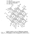
- Fig. 3 shows schematically a part of a substrate for thin film transistors when the picture element array of Fig. 1 is applied to a colour liquid crystal display of a switching element lamination system
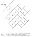
- Fig. 4 shows a part of a colour filter substrate disposed parallel to the thin film transistor substrate of Fig. 3 so as to cover the transistor substrate.
- the space between the thin film transistor substrate shown in Fig. 3 and the colour filter substrate shown in Fig. 4 is filled with a liquid crystal.
- a transparent common electrode (not shown) entirely covers the colour filter substrate.
- Each picture element has a transparent picture element electrode 12; a colour filter 14 facing the picture element electrode 12 across the liquid crystal; and a thin film transistor 16 whose gate is connected to the gate line (scanning line) 10, whose drain is connected to the data line (signal line) 20, and whose source is connected to the transparent electrode 12.
- the colour filter 14 includes a red filter which transmits only red light for a red picture element, a green filter which transmits only green light for a green picture element, and a blue filter which transmits only blue light for a blue picture element.
- R, G and B represent red, green and blue filters, respectively.
- the thin film transistor substrate and the colour filter substrate are so constructed that each picture element electrode 12 is aligned with the corresponding colour filter 14.
- Fig. 3 although a plurality of gate lines have the same reference number 10, and a plurality of data lines have the same reference number 20, each gate line 10 and data line 20 can be driven independently, and consequently, each picture element can be driven independently.
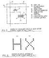
- Fig. 5 shows an equivalent circuit of one picture element of the colour liquid crystal display shown in Figs. 3 and 4.
- the same reference numbers are given to the same components of Figs. 3 and 4.
- the reference numbers 18, 22 and 24 designate a colour picture element, a liquid crystal layer and a common transparent electrode respectively.
- a data voltage is applied to each data line 20 separately, then a gate voltage is applied to the first gate line 10 to turn all the thin film transistors connected to this gate line on, and to place the liquid crystal layer 22 of each picture element in the light transmission or light shielding condition. Then, the voltage on the first gate line 10 is removed, and a data voltage is applied to each data line 20 separately and in the same manner as in the above case. A gate voltage is then applied to the second gate line 10. Even if the gate and data voltages are removed, the data voltage (accurately, the charge corresponding to the data voltage) is accumulated in the liquid crystal layer 22 with little attenuation, and the display such as a still picture can be obtained.
- Figs. 6 (a) and 6 (b) shows "H” and "X” monochromatically displayed in red, green or blue by the colour display using the colour picture element array shown in Fig. 1, for example, represented by the colour liquid crystal display shown in Figs. 3, 4 and 5.
- the display quality of horizontal, vertical and oblique lines can be made almost the same.
- the distance between (the centres of) picture elements of different colours arrayed in the direction of 45°from the horizontal direction is the same and the size of the picture elements is also the same in the above embodiment, these are not necessarily the same.
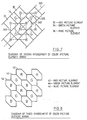
- Fig. 7 shows, the area of the blue picture elements, which have low brightness, can be increased, and the area of the green picture elements, which have high brightness, can be decreased.
- red, green and blue picture elements 32, 34 and 36 must be arranged in the direction of line 38D so that they are centred on the corners of the squares 32S, 34S and 36S whose diagonals all lie along the line 38D.
- the display quality of lines can be uniform regardless of colours even if characters or patterns on different locations are displayed as red, green or blue.
- display is usually made in either one colour of red, green or blue, the sizes of three squares at the corners of which red, green and blue picture elements are positioned may be different from each other.
- the rectangle at the corners of which the colour picture elements are centred does not need to be geometrically square.
- the picture elements are of rectangular shape in view of the effective area of a picture element being large and of gate and data line wiring being easy, the shape is not limited to rectangular, but may be of various shapes; for example, as shown in Fig. 8, red, green and blue picture elements 42, 44 and 46 may be hexagonal.
- Figs. 3, 4 and 5 relate to a liquid crystal display using thin film transistors as switching elements
- the invention can be applied to a liquid crystal display using other non-linear switching elements such as thin film diodes.
- application of the invention is not limited to liquid crystal displays, as it can be applied to other colour displays such as electrochromic displays.
- the invention can be applied to any type of display having three types of colour picture elements of colours which are different from each other.
- the colours of the picture elements are not limited to red, green and blue.
Landscapes
- Physics & Mathematics (AREA)
- Nonlinear Science (AREA)
- Crystallography & Structural Chemistry (AREA)
- Signal Processing (AREA)
- Mathematical Physics (AREA)
- Chemical & Material Sciences (AREA)
- Engineering & Computer Science (AREA)
- Multimedia (AREA)
- General Physics & Mathematics (AREA)
- Optics & Photonics (AREA)
- Liquid Crystal (AREA)
- Devices For Indicating Variable Information By Combining Individual Elements (AREA)
- Optical Filters (AREA)
Applications Claiming Priority (2)
| Application Number | Priority Date | Filing Date | Title |
|---|---|---|---|
| JP19543587A JPS6455582A (en) | 1987-08-06 | 1987-08-06 | Color display device |
| JP195435/87 | 1987-08-06 |
Publications (3)
| Publication Number | Publication Date |
|---|---|
| EP0302653A2 true EP0302653A2 (de) | 1989-02-08 |
| EP0302653A3 EP0302653A3 (en) | 1990-03-21 |
| EP0302653B1 EP0302653B1 (de) | 1993-09-15 |
Family
ID=16341011
Family Applications (1)
| Application Number | Title | Priority Date | Filing Date |
|---|---|---|---|
| EP88306901A Expired - Lifetime EP0302653B1 (de) | 1987-08-06 | 1988-07-27 | Farbeanzeige |
Country Status (5)
| Country | Link |
|---|---|
| US (1) | US4986637A (de) |
| EP (1) | EP0302653B1 (de) |
| JP (1) | JPS6455582A (de) |
| CA (1) | CA1309521C (de) |
| DE (1) | DE3884099T2 (de) |
Cited By (4)
| Publication number | Priority date | Publication date | Assignee | Title |
|---|---|---|---|---|
| US5317409A (en) * | 1991-12-03 | 1994-05-31 | North American Philips Corporation | Projection television with LCD panel adaptation to reduce moire fringes |
| WO1994023532A1 (en) * | 1993-04-05 | 1994-10-13 | Antti Aarni Tapani Iivanainen | Improving spatiotemporal resolution and enhancing motion by interlacing |
| EP3067736A1 (de) * | 2015-03-11 | 2016-09-14 | Samsung Display Co., Ltd. | Anzeigevorrichtung mit reduzierter rahmenbreite und verfahren zu deren herstellung |
| US20220146896A1 (en) * | 2019-07-31 | 2022-05-12 | Japan Display Inc. | Display device |
Families Citing this family (29)
| Publication number | Priority date | Publication date | Assignee | Title |
|---|---|---|---|---|
| FR2637407B1 (fr) * | 1988-09-30 | 1994-02-11 | Commissariat A Energie Atomique | Procede d'affichage de niveaux de gris sur un ecran a cristaux liquides ferroelectriques a phase smectique chirale |
| JPH03201788A (ja) * | 1989-12-28 | 1991-09-03 | Nippon Philips Kk | カラー表示装置 |
| KR910016199A (ko) * | 1990-02-27 | 1991-09-30 | 이헌조 | 비데오 프린터의 결상장치 |
| JPH04177220A (ja) * | 1990-11-09 | 1992-06-24 | Sharp Corp | カラー液晶表示装置 |
| US5146356A (en) * | 1991-02-04 | 1992-09-08 | North American Philips Corporation | Active matrix electro-optic display device with close-packed arrangement of diamond-like shaped |
| JP2830531B2 (ja) * | 1991-08-20 | 1998-12-02 | ソニーケミカル株式会社 | 液晶シール材用接着剤 |
| GB9122173D0 (en) * | 1991-10-18 | 1991-11-27 | Philips Electronic Associated | Liquid crystal colour display device |
| JPH07261166A (ja) * | 1994-03-23 | 1995-10-13 | Hideo Yamamoto | 液晶表示装置のカラーフィルター画素の配列方法 |
| JPH08122767A (ja) * | 1994-10-28 | 1996-05-17 | Nec Kagoshima Ltd | カラー液晶ディスプレイ |
| GB2309572A (en) | 1996-01-26 | 1997-07-30 | Sharp Kk | Spatial light modulator display |
| US6023315A (en) * | 1995-07-04 | 2000-02-08 | Sharp Kabushiki Kaisha | Spatial light modulator and directional display |
| KR100218293B1 (ko) * | 1995-12-08 | 1999-09-01 | 구본준 | 박막트랜지스터 액정표시소자 및 그의 제조방법 |
| KR100338007B1 (ko) * | 1997-09-30 | 2002-10-11 | 삼성전자 주식회사 | 액정 표시 장치 및 그의 구동 방법 |
| JP3625396B2 (ja) * | 1999-06-10 | 2005-03-02 | シャープ株式会社 | 表示装置 |
| JP2001154609A (ja) * | 1999-12-01 | 2001-06-08 | Kawasaki Steel Corp | 表示素子 |
| JP3613257B2 (ja) * | 2001-05-02 | 2005-01-26 | セイコーエプソン株式会社 | カラー表示用基板、カラーフィルタ用基板、カラー発光用基板、カラー表示用基板の製造方法、電気光学装置、電子機器 |
| KR100878280B1 (ko) * | 2002-11-20 | 2009-01-13 | 삼성전자주식회사 | 4색 구동 액정 표시 장치 및 이에 사용하는 표시판 |
| KR101309139B1 (ko) * | 2003-12-29 | 2013-09-17 | 엘지디스플레이 주식회사 | 어레이 기판 및 이를 포함하는 액정표시장치 |
| WO2006015511A1 (fr) * | 2004-08-10 | 2006-02-16 | Quanta Display Inc. | Panneau afficheur a cristaux liquides avec des marques visibles d’exactitude de coupe |
| JPWO2008072704A1 (ja) * | 2006-12-14 | 2010-04-02 | 京セラ株式会社 | 画像表示装置 |
| TWI384308B (zh) * | 2009-07-01 | 2013-02-01 | Au Optronics Corp | 顯示裝置及顯示驅動方法 |
| JP5413278B2 (ja) * | 2010-04-01 | 2014-02-12 | セイコーエプソン株式会社 | 斜方蒸着基板、液晶装置、液晶装置の製造方法、投射型表示装置 |
| CN102759819B (zh) * | 2012-07-13 | 2014-10-29 | 京东方科技集团股份有限公司 | 一种彩膜基板、阵列基板、液晶面板及液晶显示装置 |
| KR102220152B1 (ko) * | 2014-03-13 | 2021-02-26 | 삼성디스플레이 주식회사 | 표시 장치 및 그 구동 방법 |
| KR102144767B1 (ko) | 2014-06-02 | 2020-08-31 | 삼성디스플레이 주식회사 | 표시 패널 및 이를 포함하는 표시 장치 |
| CN104037201B (zh) * | 2014-06-11 | 2017-02-01 | 上海和辉光电有限公司 | 像素阵列、显示器以及将图像呈现于显示器上的方法 |
| KR102500994B1 (ko) * | 2014-10-17 | 2023-02-16 | 가부시키가이샤 한도오따이 에네루기 켄큐쇼 | 터치 패널 |
| JP6654280B2 (ja) * | 2015-01-14 | 2020-02-26 | 天馬微電子有限公司 | 画素アレイ及び電気光学装置並びに電気機器並びに画素アレイの駆動方法 |
| KR20260102366A (ko) * | 2024-12-24 | 2026-07-01 | 엘지디스플레이 주식회사 | 표시 장치 |
Family Cites Families (13)
| Publication number | Priority date | Publication date | Assignee | Title |
|---|---|---|---|---|
| US4006968A (en) * | 1975-05-02 | 1977-02-08 | Hughes Aircraft Company | Liquid crystal dot color display |
| GB1529711A (en) * | 1975-07-01 | 1978-10-25 | Rca Corp | Optical etc phase filters producing near-field patterns |
| JPS5414119A (en) * | 1977-07-05 | 1979-02-02 | Seiko Epson Corp | Liquid crystal display panel for television |
| JPS5484997A (en) * | 1978-09-27 | 1979-07-06 | Hitachi Ltd | Liquid crystal color-matrix display device |
| JPS55118077A (en) * | 1979-03-05 | 1980-09-10 | Hitachi Ltd | Color display unit |
| JPS599636A (ja) * | 1982-07-07 | 1984-01-19 | Seiko Epson Corp | 液晶表示体 |
| JPS5961818A (ja) * | 1982-10-01 | 1984-04-09 | Seiko Epson Corp | 液晶表示装置 |
| JPS59111196A (ja) * | 1982-12-15 | 1984-06-27 | シチズン時計株式会社 | カラ−表示装置 |
| JPS60218626A (ja) * | 1984-04-13 | 1985-11-01 | Sharp Corp | カラ−液晶表示装置 |
| JPS6153684A (ja) * | 1984-08-23 | 1986-03-17 | ソニー株式会社 | 液晶デイスプレイ装置 |
| JPS6170501A (ja) * | 1984-09-14 | 1986-04-11 | Matsushita Electric Ind Co Ltd | カラ−フイルタ− |
| JPS61173293A (ja) * | 1985-01-29 | 1986-08-04 | 松下電器産業株式会社 | デイジタル駆動方式カラ−デイスプレイ装置 |
| DE8512243U1 (de) * | 1985-04-25 | 1986-10-23 | Klimsch & Co KG, 6000 Frankfurt | Optisches Filter |
-
1987
- 1987-08-06 JP JP19543587A patent/JPS6455582A/ja active Granted
-
1988
- 1988-07-13 US US07/218,731 patent/US4986637A/en not_active Expired - Lifetime
- 1988-07-22 CA CA000572878A patent/CA1309521C/en not_active Expired - Lifetime
- 1988-07-27 EP EP88306901A patent/EP0302653B1/de not_active Expired - Lifetime
- 1988-07-27 DE DE88306901T patent/DE3884099T2/de not_active Expired - Fee Related
Cited By (8)
| Publication number | Priority date | Publication date | Assignee | Title |
|---|---|---|---|---|
| US5317409A (en) * | 1991-12-03 | 1994-05-31 | North American Philips Corporation | Projection television with LCD panel adaptation to reduce moire fringes |
| WO1994023532A1 (en) * | 1993-04-05 | 1994-10-13 | Antti Aarni Tapani Iivanainen | Improving spatiotemporal resolution and enhancing motion by interlacing |
| EP3067736A1 (de) * | 2015-03-11 | 2016-09-14 | Samsung Display Co., Ltd. | Anzeigevorrichtung mit reduzierter rahmenbreite und verfahren zu deren herstellung |
| CN105974626A (zh) * | 2015-03-11 | 2016-09-28 | 三星显示有限公司 | 显示装置 |
| US10488684B2 (en) | 2015-03-11 | 2019-11-26 | Samsung Display Co., Ltd. | Display apparatus having a reduced-width bezel and method of manufacturing the same |
| US20220146896A1 (en) * | 2019-07-31 | 2022-05-12 | Japan Display Inc. | Display device |
| US11656513B2 (en) * | 2019-07-31 | 2023-05-23 | Japan Display Inc. | Display device |
| US11988928B2 (en) | 2019-07-31 | 2024-05-21 | Japan Display Inc. | Display device |
Also Published As
| Publication number | Publication date |
|---|---|
| EP0302653B1 (de) | 1993-09-15 |
| CA1309521C (en) | 1992-10-27 |
| DE3884099D1 (de) | 1993-10-21 |
| JPH0444249B2 (de) | 1992-07-21 |
| DE3884099T2 (de) | 1994-04-21 |
| EP0302653A3 (en) | 1990-03-21 |
| JPS6455582A (en) | 1989-03-02 |
| US4986637A (en) | 1991-01-22 |
Similar Documents
| Publication | Publication Date | Title |
|---|---|---|
| EP0302653B1 (de) | Farbeanzeige | |
| US11424297B2 (en) | Display panel having multiple display regions and display apparatus | |
| US4811003A (en) | Alternating parallelogram display elements | |
| EP0189214B1 (de) | Aufbau eines Flüssigkristall-Mehrfarbenanzeigepaneels | |
| US4642619A (en) | Non-light-emitting liquid crystal color display device | |
| US5530570A (en) | Color liquid crystal display arrangement with elongated color filters | |
| JP3349935B2 (ja) | アクティブマトリクス型液晶表示装置 | |
| EP0186086B1 (de) | Paneel für Farbanzeige | |
| US5461503A (en) | Color matrix display unit with double pixel area for red and blue pixels | |
| CN100570449C (zh) | 彩色显示装置 | |
| EP0347187B1 (de) | Farbanzeigetafel | |
| US20070195253A1 (en) | Liquid crystal display device with one pixel electrode having a plurality of generally circular patterns in each pixel region | |
| US10223954B2 (en) | Array substrate and method for manufacturing the same, and display apparatus | |
| GB2213308A (en) | Pixel configuration | |
| CN110989871A (zh) | 阵列基板、显示面板和显示装置 | |
| JP2002006303A (ja) | カラー液晶表示装置 | |
| EP0485216A2 (de) | Flüssigkristallfarbanzeige | |
| KR100495719B1 (ko) | 화상표시장치및그화소배열방법 | |
| US5235447A (en) | Color matrix screen with colored filters in a triad or delta layout with two sub-pixels per color | |
| JPS60207118A (ja) | マトリクス形フルカラ−液晶表示パネル | |
| JPH01169433A (ja) | 液晶ディスプレイパネル | |
| CN113644107B (zh) | 阵列基板、显示面板及显示设备 | |
| KR20020010209A (ko) | 화소 배열 구조 및 이를 포함하는 액정 표시 장치용 기판 | |
| JPH02173783A (ja) | 平形パネル表示装置のカラーマトリツクスアレイ | |
| JPS63282717A (ja) | アクティブマトリックス型液晶表示装置 |
Legal Events
| Date | Code | Title | Description |
|---|---|---|---|
| PUAI | Public reference made under article 153(3) epc to a published international application that has entered the european phase |
Free format text: ORIGINAL CODE: 0009012 |
|
| AK | Designated contracting states |
Kind code of ref document: A2 Designated state(s): DE FR GB IT |
|
| 17P | Request for examination filed |
Effective date: 19890619 |
|
| PUAL | Search report despatched |
Free format text: ORIGINAL CODE: 0009013 |
|
| AK | Designated contracting states |
Kind code of ref document: A3 Designated state(s): DE FR GB IT |
|
| 17Q | First examination report despatched |
Effective date: 19921123 |
|
| GRAA | (expected) grant |
Free format text: ORIGINAL CODE: 0009210 |
|
| AK | Designated contracting states |
Kind code of ref document: B1 Designated state(s): DE FR GB IT |
|
| PG25 | Lapsed in a contracting state [announced via postgrant information from national office to epo] |
Ref country code: IT Free format text: LAPSE BECAUSE OF FAILURE TO SUBMIT A TRANSLATION OF THE DESCRIPTION OR TO PAY THE FEE WITHIN THE PRESCRIBED TIME-LIMIT;WARNING: LAPSES OF ITALIAN PATENTS WITH EFFECTIVE DATE BEFORE 2007 MAY HAVE OCCURRED AT ANY TIME BEFORE 2007. THE CORRECT EFFECTIVE DATE MAY BE DIFFERENT FROM THE ONE RECORDED. Effective date: 19930915 |
|
| REF | Corresponds to: |
Ref document number: 3884099 Country of ref document: DE Date of ref document: 19931021 |
|
| ET | Fr: translation filed | ||
| PLBE | No opposition filed within time limit |
Free format text: ORIGINAL CODE: 0009261 |
|
| STAA | Information on the status of an ep patent application or granted ep patent |
Free format text: STATUS: NO OPPOSITION FILED WITHIN TIME LIMIT |
|
| 26N | No opposition filed | ||
| PGFP | Annual fee paid to national office [announced via postgrant information from national office to epo] |
Ref country code: GB Payment date: 20010702 Year of fee payment: 14 |
|
| PGFP | Annual fee paid to national office [announced via postgrant information from national office to epo] |
Ref country code: FR Payment date: 20010717 Year of fee payment: 14 |
|
| PGFP | Annual fee paid to national office [announced via postgrant information from national office to epo] |
Ref country code: DE Payment date: 20010723 Year of fee payment: 14 |
|
| REG | Reference to a national code |
Ref country code: GB Ref legal event code: IF02 |
|
| PG25 | Lapsed in a contracting state [announced via postgrant information from national office to epo] |
Ref country code: GB Free format text: LAPSE BECAUSE OF NON-PAYMENT OF DUE FEES Effective date: 20020727 |
|
| PG25 | Lapsed in a contracting state [announced via postgrant information from national office to epo] |
Ref country code: DE Free format text: LAPSE BECAUSE OF NON-PAYMENT OF DUE FEES Effective date: 20030201 |
|
| GBPC | Gb: european patent ceased through non-payment of renewal fee |
Effective date: 20020727 |
|
| PG25 | Lapsed in a contracting state [announced via postgrant information from national office to epo] |
Ref country code: FR Free format text: LAPSE BECAUSE OF NON-PAYMENT OF DUE FEES Effective date: 20030331 |
|
| REG | Reference to a national code |
Ref country code: FR Ref legal event code: ST |