EP0302727A2 - Überwachungsgerät - Google Patents
Überwachungsgerät Download PDFInfo
- Publication number
- EP0302727A2 EP0302727A2 EP88307210A EP88307210A EP0302727A2 EP 0302727 A2 EP0302727 A2 EP 0302727A2 EP 88307210 A EP88307210 A EP 88307210A EP 88307210 A EP88307210 A EP 88307210A EP 0302727 A2 EP0302727 A2 EP 0302727A2
- Authority
- EP
- European Patent Office
- Prior art keywords
- electrode
- capacitor
- amplifying circuit
- inverting input
- article
- Prior art date
- Legal status (The legal status is an assumption and is not a legal conclusion. Google has not performed a legal analysis and makes no representation as to the accuracy of the status listed.)
- Withdrawn
Links
Images


Classifications
-
- G—PHYSICS
- G01—MEASURING; TESTING
- G01N—INVESTIGATING OR ANALYSING MATERIALS BY DETERMINING THEIR CHEMICAL OR PHYSICAL PROPERTIES
- G01N27/00—Investigating or analysing materials by the use of electric, electrochemical, or magnetic means
- G01N27/02—Investigating or analysing materials by the use of electric, electrochemical, or magnetic means by investigating impedance
- G01N27/22—Investigating or analysing materials by the use of electric, electrochemical, or magnetic means by investigating impedance by investigating capacitance
- G01N27/24—Investigating the presence of flaws
Definitions
- This invention relates to monitoring apparatus and in particular apparatus for monitoring the dielectric constant of an article.
- monitoring apparatus which comprises an amplifying circuit including a capacitor between the electrodes of which an article is moved in use and in which the gain of the amplifying circuit varies with the capacitance of the capacitor so that the peak value of the output signal of the amplifying circuit varies with the dielectric constant of the article between the capacitor electrodes.
- a simple amplifying circuit including for example an operational amplifier with one of the inputs at a constant electrical potential and the other input connected to one electrode of the capacitor so that changes in dielectric constant between the capacitor plates affect the gain of the amplifier.
- the peak output values from the amplifier are found to vary with the dielectric constant between the capacitor electrodes and as one input of the operational amplifier is kept at a constant potential stray capacitances have minimal effect on the output signals from the amplifiers.
- the amplifying circuit includes an operational amplifier with the non-inverting input connected to a constant electrical ground potential and the inverting input connected to one electrode of the capacitor.
- a feedback loop is present between the operational amplifier output and the inverting input. This has the effect of forcing the inverting input to the same potential as the non-inverting input, usually ground.
- the advantage of using this technique is that the capacitor electrode connected to the inverting input remains at a constant potential and therefore the electric field between the capacitor plates remains substantially constant.
- a guard electrode would typically surround the capacitor electrode connected to the inverting input and would be maintained at substantially the same constant potential. This has the advantage of helping to maintain a substantially uniform electric field over the area of the article being monitored.
- an oscillating voltage signal is applied to the capacitor electrode not connected to the operational amplifier.
- a peak detecting circuit is also provided which receives the output signals from the amplifying circuit and outputs the peak values of the signals received from the amplifying circuit.
- a plurality of amplifying circuits and peak detector circuits are provided, the respective capacitors being positioned in a line transverse to the direction of movement of an article in use, the apparatus further comprising a multiplexer to which output signals from the peak detector circuits are sent. Typically the multiplexer will then feed each signal in turn to a processing unit and after processing the signals are displayed.
- each amplifying circuit preferably has substantially the same gain when the capacitance of each of the respective capacitors is substantially equal.
- each amplifying circuit is preferably substantially equal for each circuit. This creates a substantially uniform electric field of the same value between the electrodes of each capacitor.
- one electrode of each capacitor may be provided by a common plate.
- one amplifying circuit is provided which scans across the article producing signals which are then sequentially fed directly to the processing unit before being displayed.
- the article comprises a metallic layer then preferably one of the capacitor plates is provided by the metallic layer of the article.
- one electrode of the capacitor could be formed from a matrix of eiectrode pads connected electrically and configured to the shape of the article to be detected.
- the monitoring techniques and apparatus described above are particularly advantageous when monitoring the composition of articles where the thickness of the article is of the same order as the required resolution. This is typically of about 1mm to 5mm.
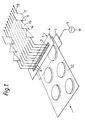
- the apparatus shown in Figure 1 comprises a continuous electrode 1 and an electrode assembly 2 which includes a number of sensing electrodes 3 and a guard electrode 4.
- the electrodes 1 and 2 are arranged so that their planar surfaces are parallel to each other.
- each sensing electrode 3 in effect forms a capacitor with the continuous electrode 1.
- An oscillating voltage signal (typically 10V peak to peak) is applied to the continuous electrode 1 by an oscillating voltage source 5 so that the whole of the electrode 1 is at a uniform potential at any instant in time.
- the guard electrode 4 on the electrode 2 is kept at a constant potential, which can be conveniently achieved by connecting it to an electrical ground potential 6 as shown in the circuit diagram of Figure 3.
- the sensing electrodes 3 are electrically isolated from the guard electrode 4 by an electrically insulating material 7. Each sensing electrode 3 is electrically connected to the inverting input 8 of a respective operational amplifier 9 as shown in Figure 3 and the non-inverting input 10 of the operational amplifier 9 is electrically connected to the ground potential 6.
- the sensing electrodes 3 are all effectively at ground potential.
- the outputs 14 of the amplifiers 9 are each connected to respective peak detectors 15 which in turn are connected to respective sample and hold circuits 17.
- the outputs 18 from the sample and hold circuits 17 are each connected to a con on multiplexer 19 ( Figure 2) which is in turn connected to an analogue to digital converter 20.
- the analogue to digital converter 20 is connected to a processing unit or computer 21 and a display 24.
- an article 22 in this example a blisterpack containing pills is passed between the electrodes 1, 2.
- the capacitance between the sensors 3 and the electrode 1 is dependent on the dielectric constant of the article between the sensors 3 and the electrode 1, and therefore changes as the blisterpack passes through the electrodes 1, 2 due to the presence or absence of pills within the blisterpack pockets.
- the peak value of the output signal 14 from each amplifier 9 varies directly with the dielectric constant between the sensing electrode 3 to which it is connected and the electrode 1.
- the output signal 14 is then fed to the peak detector 15 which senses the maximum of the output signal 14 at regular intervals and provides a corresponding maximum value output signal 16 which varies directly with the dielectric constant of the article.
- the output signal 16 from the peak detector 15 is then fed via the sample and hold circuit 17 to the multiplexer 19.
- the output 23 of the multiplexer 19 is continuously cycled through all of the outputs 18 from the sample and hold circuits 17 and this output 23 is then fed to the analogue to digital converter 20.
- the analogue to digital converter 20 converts the analogue peak voltage signals to digital signals and then feeds these digital signals to the processing unit 21.
- the cycling of the multiplexer inputs is duplicated by the raster display on the monitor 24 which then displays an image of the variation in dielectric constant as the blisterpack is moved between the electrodes 1, 3.
- the signal from any one of the electrodes 3 will contain signal contributions not only from the material directly underneath that electrode but also from material under adjacent electrodes a resulting image produced from these signals could be blurred.
- a deconvolution operation is performed on the signals by the processing unit 21.
- the process of deconvolution is well known in digital image processing and only a brief description of the procedure is given below. A detailed description of the procedure can be found in "Fourier Transforms and their Physical Applications" by D.C.Champeney and published by Academic Press.
- d(j,k) the actual, nonblurred, representation of the distribution of dielectric. This can be done as follows, by first taking the fourier transform of both sides of the above equation.
- d(j,k) i(j,k) * F ⁇ 1(1/H(u,v)) where F ⁇ 1 denotes the inverse fourier transform.
- F ⁇ 1(1/H(u,v)) is a two dimensional function which can be denoted as f(j,k).
- the nonblurred image of the article 22 is displayed on a screen 24. An operator can then determine from the displayed image whether there are any broken or missing pills in the blisterpack.
- the apparatus shown in Figure 4 operates on the same principles as the apparatus shown in Figure 1 the difference between the two examples being that in Figure 4 only a single sensing eiectrode 3 is used instead of a number of sensing electrodes 3. Therefore there is only one amplifier 9, one peak detector 15 and one sample and hold circuit 17. Thus the output 18 from the sample and hold circuit 17 can be connected directly to the analogue to digital converter 20 without the use of a multiplexer 19.
- an oscillating voltage signal is applied by the oscillator 5 to the continuous electrode 1 as before and an article 22 is passed between the continuous electrode 1 and the sensing electrode 3.
- the sensing electrode 3 is scanned backwards and forwards across the article 22 to produce output signals which are representative of the dielectric constant of the article and these are then processed using the deconvolution procedure in the processing unit 21 and imaged on the screen 24 as before.
- the apparatus shown in Figure 5 can be used with either the apparatus in Figure 4 or the apparatus in Figure 1.
- the article 22 is again a blisterpack but this time with a metallic backing foil 25.
- the metallic backing foil 25 is a conductor a potential applied to the continuous electrode 1 would be screened from the sensing electrode 3 by the backing foil 25.
- the oscillating voltage must be applied to the backing foil 25 of the blisterpack 22.
- the backing foil 25 acts as the continuous electrode 1.
- the voltage applied to the foil 25 would typically be 10 volts peak to peak and as the foil would be grounded to earth via a 10 ohm resistor 26 there would be no danger of electrocution while using this apparatus.
- the amplifier 9 and the other components of the detecting apparatus are identical to that used in the apparatus shown in Figures 1 and 4.
- the electrode 3 is a configured electrode which comprises a matrix of individual sensing pads 31 which form part of a sensing head 34. Each sensing pad 31 which forms part of the configured electrode 3 is electrically connected to its neighbours by a connection 32.
- the guard electrode 4 in this example also comprises a number of individual sensing pads 31 on the sensing head 34 which are again electrically connected to each other by means of connections 32. None of the connections 32 connect the sensing pads 31 of the guard electrode 4 to the sensing pads 31 of the configured electrode 3. Hence, the configured electrode 3 is electrically isolated from the guard electrode 4.
- the guard electrode 4 comprises the cross hatched pads, that is the four sensing pads 31 at each corner of the sensing head 34 and the peripheral pads of the sensing head 34, between the four pads of each corner of the sensing head 34.
- the configured electrode 3 is formed from the remainder of the pads 31, that is all the pads 31 except for the cross hatched pads, which are the four pads at each corner and the pads which form the periphery of the sensing head 34.
- connections 32 are removable so that the configuration of the configured electrode 3 may be modified to suit a particular application.
- the configured electrode 3 could be configured to the same shape as the article 22 to be monitored by positioning the connections 32 appropriately.
- the electrode 3 could be configured so as to be narrower than the article 22 in the direction of the third of the article 22 but have the same width as the article 22 in the direction perpendicular to the direction of the third. This would give better resolution oi the articles 22 by the apparatus.
- the type of configured electrode shown in Figure 6 is particularly suitable for the detection of large multiple products such as biscuits in packs.
- this apparatus and in particular the sensing circuit and amplifying circuit shown in Figure 3 are that because the sensing electrodes 3 are all held at the same potential stray capacitances which may be present nearby do not affect the sensitivity or resolution of the apparatus.
- this circuit is found to be very accurate and capable of detecting differences in capacitance of the order of 10 ⁇ 3 pF when the average capacitance present is of the order 10 ⁇ 2 pF.
- the surface area of the sensing electrodes 3 is typically .04 cm2 and this will give a resolution of 2mm when the top surface of the article is 2 mm from the sensing electrodes 3 and the thickness of the article is of the same order as the resolution.
- the apparatus and circuit described here are also capable of monitoring the surface topology of an article.
- the apparatus may also be used for monitoring laminated board for bonding problems and reading digitised bar codes.
Landscapes
- Chemical & Material Sciences (AREA)
- Chemical Kinetics & Catalysis (AREA)
- Electrochemistry (AREA)
- Physics & Mathematics (AREA)
- Health & Medical Sciences (AREA)
- Life Sciences & Earth Sciences (AREA)
- Analytical Chemistry (AREA)
- Biochemistry (AREA)
- General Health & Medical Sciences (AREA)
- General Physics & Mathematics (AREA)
- Immunology (AREA)
- Pathology (AREA)
- Investigating Or Analyzing Materials By The Use Of Electric Means (AREA)
- Measurement Of Resistance Or Impedance (AREA)
- Fixed Capacitors And Capacitor Manufacturing Machines (AREA)
Applications Claiming Priority (2)
| Application Number | Priority Date | Filing Date | Title |
|---|---|---|---|
| GB878718606A GB8718606D0 (en) | 1987-08-06 | 1987-08-06 | Monitoring apparatus |
| GB8718606 | 1987-08-06 |
Publications (2)
| Publication Number | Publication Date |
|---|---|
| EP0302727A2 true EP0302727A2 (de) | 1989-02-08 |
| EP0302727A3 EP0302727A3 (de) | 1990-06-27 |
Family
ID=10621894
Family Applications (1)
| Application Number | Title | Priority Date | Filing Date |
|---|---|---|---|
| EP88307210A Withdrawn EP0302727A3 (de) | 1987-08-06 | 1988-08-04 | Überwachungsgerät |
Country Status (6)
| Country | Link |
|---|---|
| US (1) | US4922181A (de) |
| EP (1) | EP0302727A3 (de) |
| JP (1) | JPH0196569A (de) |
| AU (1) | AU612087B2 (de) |
| CA (1) | CA1296769C (de) |
| GB (1) | GB8718606D0 (de) |
Cited By (13)
| Publication number | Priority date | Publication date | Assignee | Title |
|---|---|---|---|---|
| GB2229539B (en) * | 1987-10-02 | 1992-05-13 | Detection Systems Pty Ltd | Capacitive material presence detecting apparatus |
| DE4243206A1 (de) * | 1992-12-19 | 1994-06-23 | Hoefliger & Oehlmann Ges Zum B | Verfahren und Vorrichtung zum Überprüfen einer automatischen Abfüllanlage auf korrektes Befüllen |
| US5426373A (en) * | 1992-09-30 | 1995-06-20 | The United States Of America As Represented By The Secretary Of The Navy | Two electrode device for determining electrical properties of a material on a metal substratum |
| FR2715741A1 (fr) * | 1994-02-03 | 1995-08-04 | Massachusetts Inst Technology | Détecteur de la position d'un objet et de la distribution d'une masse. |
| US5650729A (en) * | 1992-10-19 | 1997-07-22 | De La Rue Systems Limited | Conductive strip detector |
| GB2313194A (en) * | 1996-05-08 | 1997-11-19 | John Allen | Player detection and location |
| US5844415A (en) * | 1994-02-03 | 1998-12-01 | Massachusetts Institute Of Technology | Method for three-dimensional positions, orientation and mass distribution |
| US5936412A (en) * | 1994-02-03 | 1999-08-10 | Massachusetts Institute Of Technology | Method for resolving presence, orientation and activity in a defined space |
| US5948031A (en) * | 1996-02-23 | 1999-09-07 | Nec Technologies, Inc. | Vehicle passenger sensing system and method |
| US6161070A (en) * | 1996-02-23 | 2000-12-12 | Nec Home Electronics, Inc. | Passenger detection system |
| EP1193177A1 (de) * | 2000-09-27 | 2002-04-03 | Uhlmann VisioTec GmbH | Verfahren zur Überprüfung der Füllung von Höfen oder Näpfen einer Blisterverpackung für Arzneimittel |
| DE102004018630A1 (de) * | 2004-04-16 | 2005-11-10 | Pepperl + Fuchs Gmbh | Vorrichtung, Sensoranordnung und Verfahren zur kapazitiven Positionserfassung eines Zielobjekts |
| EP2562535A1 (de) * | 2006-08-28 | 2013-02-27 | Detection Systems Pty.Ltd. | Detektionsvorrichtung und -verfahren |
Families Citing this family (15)
| Publication number | Priority date | Publication date | Assignee | Title |
|---|---|---|---|---|
| DE4009697A1 (de) * | 1990-03-27 | 1991-10-02 | Fife Gmbh | Vorrichtung zum beruehrungslosen erfassen der lage eines sich bewegenden materialbandes |
| US5218309A (en) * | 1990-06-25 | 1993-06-08 | The United States Of America As Represented By The Secretary Of Agriculture | Single kernel, seed, nut, or fruit dielectric moisture content measurement |
| US5135113A (en) * | 1991-04-01 | 1992-08-04 | Modern Controls, Inc. | High-speed tablet sorting machine |
| US5321366A (en) * | 1992-08-31 | 1994-06-14 | Murata Mfg. Co. Ltd. | Capacitance sensor apparatus of divided multi-electrode type |
| US5373245A (en) * | 1993-07-12 | 1994-12-13 | The United States Of America As Represented By The Administrator Of The National Aeronautics And Space Administration | Capaciflector camera |
| DE19511646C2 (de) * | 1995-03-30 | 1999-01-07 | Fife Gmbh | Vorrichtung zum berührungslosen Erfassen der Lage eines laufenden Materialbandes |
| US5585732A (en) * | 1995-06-07 | 1996-12-17 | Mississippi State University | Detector for heterogeneous materials |
| JP3620998B2 (ja) * | 1999-06-08 | 2005-02-16 | 株式会社ニレコ | 導電性物体の端部検出装置 |
| CA2629632C (en) * | 2007-02-16 | 2013-06-18 | Countlab Inc. | A container filling machine |
| US8006468B2 (en) * | 2008-04-14 | 2011-08-30 | Countlab Inc. | Container filling machine having vibration trays |
| US8225925B2 (en) * | 2008-12-02 | 2012-07-24 | Countlab Inc. | Discrete article spacing apparatus for vibration trays |
| US20130042943A1 (en) | 2011-08-18 | 2013-02-21 | Countlab, Inc. | Container filling machine |
| US10083594B2 (en) * | 2016-04-08 | 2018-09-25 | QuantaEd, LLC | Apparatus and method for improved drug regimen compliance |
| WO2020046207A1 (en) * | 2018-08-31 | 2020-03-05 | National University Of Singapore | Method and system for integrity testing of blister packages |
| WO2021029825A1 (en) * | 2019-08-15 | 2021-02-18 | National University Of Singapore | Method and system for integrity testing of packages |
Family Cites Families (13)
| Publication number | Priority date | Publication date | Assignee | Title |
|---|---|---|---|---|
| US3391337A (en) * | 1965-06-21 | 1968-07-02 | Laucks Lab Inc | Scanning-type moisture detection system with sequential solid-state switching and synchronous material marking means |
| US3519922A (en) * | 1965-12-16 | 1970-07-07 | Nash & Harrison Ltd | Apparatus for detecting abrupt change in the thickness of sheet material |
| US3497802A (en) * | 1966-02-04 | 1970-02-24 | Industrial Nucleonics Corp | Method and apparatus for detecting narrow streaks and the average value of a property over a relatively wide region utilizing a single probe |
| GB1370233A (en) * | 1972-01-06 | 1974-10-16 | Goring Kerr Ltd | Electrical sorting apparatus |
| US4031752A (en) * | 1976-07-19 | 1977-06-28 | Art Sanders | Web process control apparatus |
| US4190797A (en) * | 1978-03-31 | 1980-02-26 | Gould Inc. | Capacitive gauging system utilizing a low internal capacitance, high impedance amplifier means |
| US4322678A (en) * | 1978-10-30 | 1982-03-30 | Capots Larry H | Identification of materials using their complex dielectric response |
| US4377783A (en) * | 1979-10-15 | 1983-03-22 | Wagner Delmer W | Moisture detector |
| NL8101310A (nl) * | 1981-03-18 | 1982-10-18 | Skf Ind Trading & Dev | Inrichting voor het meten van de variatie van een capacitieve impedantie, waarvan het dielektricum wordt gevormd door een smeermiddel. |
| US4481616A (en) * | 1981-09-30 | 1984-11-06 | Rca Corporation | Scanning capacitance microscope |
| DE3433148C2 (de) * | 1984-09-10 | 1987-01-22 | Endress U. Hauser Gmbh U. Co, 7867 Maulburg | Anordnung zur Erfassung räumlicher Inhomogenitäten in einem Dielektrikum |
| US4733166A (en) * | 1986-03-17 | 1988-03-22 | Wagner Delmer W | Apparatus for measuring the moisture content of moving materials |
| SE456869B (sv) * | 1986-06-19 | 1988-11-07 | Electrolux Ab | Anordning foer avkaenning av antalet i ett fack efter varandra anordnade, likadana foeremaal |
-
1987
- 1987-08-06 GB GB878718606A patent/GB8718606D0/en active Pending
-
1988
- 1988-08-02 US US07/227,274 patent/US4922181A/en not_active Expired - Fee Related
- 1988-08-04 EP EP88307210A patent/EP0302727A3/de not_active Withdrawn
- 1988-08-04 AU AU20405/88A patent/AU612087B2/en not_active Ceased
- 1988-08-05 CA CA000574059A patent/CA1296769C/en not_active Expired - Lifetime
- 1988-08-06 JP JP63197002A patent/JPH0196569A/ja active Pending
Cited By (16)
| Publication number | Priority date | Publication date | Assignee | Title |
|---|---|---|---|---|
| GB2229539B (en) * | 1987-10-02 | 1992-05-13 | Detection Systems Pty Ltd | Capacitive material presence detecting apparatus |
| US5426373A (en) * | 1992-09-30 | 1995-06-20 | The United States Of America As Represented By The Secretary Of The Navy | Two electrode device for determining electrical properties of a material on a metal substratum |
| US5650729A (en) * | 1992-10-19 | 1997-07-22 | De La Rue Systems Limited | Conductive strip detector |
| DE4243206A1 (de) * | 1992-12-19 | 1994-06-23 | Hoefliger & Oehlmann Ges Zum B | Verfahren und Vorrichtung zum Überprüfen einer automatischen Abfüllanlage auf korrektes Befüllen |
| US5936412A (en) * | 1994-02-03 | 1999-08-10 | Massachusetts Institute Of Technology | Method for resolving presence, orientation and activity in a defined space |
| GB2286247A (en) * | 1994-02-03 | 1995-08-09 | Massachusetts Inst Technology | Capacitive position detection |
| US5844415A (en) * | 1994-02-03 | 1998-12-01 | Massachusetts Institute Of Technology | Method for three-dimensional positions, orientation and mass distribution |
| FR2715741A1 (fr) * | 1994-02-03 | 1995-08-04 | Massachusetts Inst Technology | Détecteur de la position d'un objet et de la distribution d'une masse. |
| US5948031A (en) * | 1996-02-23 | 1999-09-07 | Nec Technologies, Inc. | Vehicle passenger sensing system and method |
| US6161070A (en) * | 1996-02-23 | 2000-12-12 | Nec Home Electronics, Inc. | Passenger detection system |
| GB2313194A (en) * | 1996-05-08 | 1997-11-19 | John Allen | Player detection and location |
| EP1193177A1 (de) * | 2000-09-27 | 2002-04-03 | Uhlmann VisioTec GmbH | Verfahren zur Überprüfung der Füllung von Höfen oder Näpfen einer Blisterverpackung für Arzneimittel |
| US6757637B2 (en) | 2000-09-27 | 2004-06-29 | Uhlmann Visiotec Gmbh | Method for checking the content of pockets in a blister package |
| DE102004018630A1 (de) * | 2004-04-16 | 2005-11-10 | Pepperl + Fuchs Gmbh | Vorrichtung, Sensoranordnung und Verfahren zur kapazitiven Positionserfassung eines Zielobjekts |
| EP2562535A1 (de) * | 2006-08-28 | 2013-02-27 | Detection Systems Pty.Ltd. | Detektionsvorrichtung und -verfahren |
| US8922226B2 (en) | 2006-08-28 | 2014-12-30 | Detection Systems Pty Ltd | Production line detection apparatus and method |
Also Published As
| Publication number | Publication date |
|---|---|
| US4922181A (en) | 1990-05-01 |
| CA1296769C (en) | 1992-03-03 |
| JPH0196569A (ja) | 1989-04-14 |
| AU2040588A (en) | 1989-02-09 |
| AU612087B2 (en) | 1991-06-27 |
| EP0302727A3 (de) | 1990-06-27 |
| GB8718606D0 (en) | 1987-09-09 |
Similar Documents
| Publication | Publication Date | Title |
|---|---|---|
| US4922181A (en) | Apparatus for monitoring the dielectric constant of an article | |
| EP0503032B1 (de) | Kapazitieve sonde | |
| US4067225A (en) | Capacitance type non-contact displacement and vibration measuring device and method of maintaining calibration | |
| US5369228A (en) | Data input device with a pressure-sensitive input surface | |
| Boie | Capacitive impedance readout tactile image sensor | |
| US3466391A (en) | Electrical position resolver employing capacitive probe coupled to resistive layer containing two pairs of conductive strips energized by four different frequency signals | |
| US5373245A (en) | Capaciflector camera | |
| JP3482190B2 (ja) | 容量的な画像検出方法 | |
| KR100369094B1 (ko) | 접촉식지정소자 | |
| US7622907B2 (en) | Device, system and method for a sensing electrical circuit | |
| US4771138A (en) | Electrostatic pattern-coupled digitizer | |
| US4134063A (en) | Apparatus for the time-dependent measurement of physical quantities | |
| EP0199100B1 (de) | Eingabesystem mit elektromagnetischem Berührungssensor in einer Kathodenstrahlröhren-Anzeigevorrichtung | |
| US6388453B1 (en) | Swept-frequency dielectric moisture and density sensor | |
| US4623757A (en) | Method and apparatus for electronic touch mapping | |
| US4055726A (en) | Electrical position resolving by zero-crossing delay | |
| US4831566A (en) | Method and apparatus for calibration of a charge ratio digitizer | |
| JPS63259451A (ja) | 移動する材料ウェブに関連した水分量を制御する方法 | |
| GB2164450A (en) | Arrangement for detecting spatial inhomogeneities in a dielectric | |
| CA2467900A1 (en) | Electrode for biomedical measurements | |
| EP0978722B1 (de) | Kammförmiges Sensorelement mit Elektroden auf den Zähnen und Kantenanschlüssen auf der gegenüberliegenden Seite | |
| JPH0652206B2 (ja) | 静電容量型圧力分布測定装置 | |
| US6504387B1 (en) | Item detection/inspection arrangement | |
| US6374681B1 (en) | Electronic scanning device to measure at high speed, physical properties of large multi-dimensional arrays | |
| KR100226812B1 (ko) | 위치검출 액정표시장치 |
Legal Events
| Date | Code | Title | Description |
|---|---|---|---|
| PUAI | Public reference made under article 153(3) epc to a published international application that has entered the european phase |
Free format text: ORIGINAL CODE: 0009012 |
|
| AK | Designated contracting states |
Kind code of ref document: A2 Designated state(s): CH DE ES FR GB IT LI SE |
|
| RAP3 | Party data changed (applicant data changed or rights of an application transferred) |
Owner name: LAETUS SYSTEMS LIMITED |
|
| PUAL | Search report despatched |
Free format text: ORIGINAL CODE: 0009013 |
|
| AK | Designated contracting states |
Kind code of ref document: A3 Designated state(s): CH DE ES FR GB IT LI SE |
|
| 17P | Request for examination filed |
Effective date: 19901116 |
|
| 17Q | First examination report despatched |
Effective date: 19920416 |
|
| STAA | Information on the status of an ep patent application or granted ep patent |
Free format text: STATUS: THE APPLICATION IS DEEMED TO BE WITHDRAWN |
|
| 18D | Application deemed to be withdrawn |
Effective date: 19940830 |