EP0302926B1 - Circuit de generation de signaux de commande pour unite arithmetique et logique pour un processeur numerique - Google Patents
Circuit de generation de signaux de commande pour unite arithmetique et logique pour un processeur numerique Download PDFInfo
- Publication number
- EP0302926B1 EP0302926B1 EP88902032A EP88902032A EP0302926B1 EP 0302926 B1 EP0302926 B1 EP 0302926B1 EP 88902032 A EP88902032 A EP 88902032A EP 88902032 A EP88902032 A EP 88902032A EP 0302926 B1 EP0302926 B1 EP 0302926B1
- Authority
- EP
- European Patent Office
- Prior art keywords
- signals
- signal
- control
- data
- processor
- Prior art date
- Legal status (The legal status is an assumption and is not a legal conclusion. Google has not performed a legal analysis and makes no representation as to the accuracy of the status listed.)
- Expired - Lifetime
Links
Images




Classifications
-
- G—PHYSICS
- G06—COMPUTING OR CALCULATING; COUNTING
- G06F—ELECTRIC DIGITAL DATA PROCESSING
- G06F9/00—Arrangements for program control, e.g. control units
- G06F9/06—Arrangements for program control, e.g. control units using stored programs, i.e. using an internal store of processing equipment to receive or retain programs
- G06F9/22—Microcontrol or microprogram arrangements
- G06F9/26—Address formation of the next micro-instruction ; Microprogram storage or retrieval arrangements
- G06F9/262—Arrangements for next microinstruction selection
- G06F9/264—Microinstruction selection based on results of processing
- G06F9/267—Microinstruction selection based on results of processing by instruction selection on output of storage
Definitions
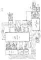
- the bus interface unit 33 includes a state machine 270, which controls the transfer of data over bus 13, and an IDAL state machine 271, which controls the transfer of data over internal IDAL bus 34.
- the bus interface unit also controls an FPP logic circuit 272 which, in turn, controls communications with the floating point processor 31.
- the bus interface unit 33 will be described in more detail below in connection with Fig. 6.
- the bus 13 includes a number of lines for transferring signals representing information among the various units connected to it.
- bus 13 includes DAL (31:0) data address lines 50, which carry DAT data and ADRS address signals. If the CPU 10, specifically the processor 30, is initiating a transfer, making it the bus master for the transfer, processor 30 first transmits the ADRS address signals over the DAL (31:0) data address lines 50 and contemporaneously transmits TR TYPE (2:0) transfer type command signals on lines 52, which indicate whether the transfer operation is a read or a write operation. A short time later, sufficient to allow the ADRS address signals and TR TYPE (2:0) transfer type command signals to settle, the processor 30 then asserts an ADRS STR address strobe signal on a line 51.
- the memory 11 In connection with this use of the CCTL cache control signal, the memory 11 asserts the CCTL cache control signal contemporaneously with its transmission of the data over the DAL data address lines 50, and maintains the CCTL cache control signal asserted until it removes the data.
- the floating point processor 31 Since the floating point processor 31 has already received the operation information in the procedure described above in connection with Fig. 2A, it is in condition to receive an operand.
- the asserted CP DAT (5:0) floating point data signal indicates to the floating point processor 31 that it is to sample the signals on selected lines of bus 13, in particular the line 51 which carries the ADRS STR address strobe signal.
- the floating point processor 31 uses the asserted condition of the ADRS STR address strobe signal to determine that the operand is being retrieved from the memory 11.
- the floating point processor 31 When the floating point processor 31 is ready to transfer the processed data, it transmits CP STA (1:0) floating point status signals representing a code to that effect, concurrently with CP DAT (5:0) floating point data signals representing the condition codes. The floating point processor 31 maintains these signals for a selected number of ticks of the CLK clock signals, and then places the data signals on the DAL data address lines 50, along with a code on lines 70 and 71 to that effect. If multiple transfers over DAL data address lines 50 to transfer the processed data signals, the floating point processor 31 transfers them synchronously with the CLK clock signals.
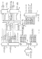
- the temporary register set 81 and working register set 82 receive similar control signals.
- the temporary register set 81 receives a set of A EN TEMP "A" enable temporary control signals for enabling the contents of selected temporary registers to be transferred to the A IN input terminal of arithmetic and logic unit 83.
- a set of W EN TEMP write enable temporary control signals enables the processed data from the W OUT output terminal of arithmetic and logic unit 83 to be stored in a selected temporary register in temporary register set 81.
- the control circuit 40 asserts the A LTH HOLD and B LTH HOLD latch hold signals when the signals on the respective signal lines have become stable to be used in generating the various W EN XX write enabling signals, so that the control circuit can proceed to generate and use a new control microinstruction, which might otherwise cause outputs of the decoders 90 and 91 to change and the signals on the signal lines to vary.
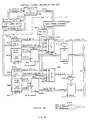
- the operations performed by arithmetic and logic unit 83 are controlled by ALU CTRL signals from ALU control circuit 84, which, in turn, is controlled by ALU OP SEL operation select signals from the control circuits 40 (Fig. 1B) of processor 30.
- the ALU control circuit 84 includes a decoder 85 in the form of a programmable logic array circuit which generates ALU CTRL CODE control code signals in response to the ALU OP SEL operation select signals.
- a decoder 86 receives the ALU OP SEL operation select signals and generates an MUL multiply signal or a DIV divide signal in response to selected encodings of the ALU OP SEL operation select signals.
- Hit buffers 111 buffer the PTE HIT (27:0) page table entry hit signals and time them in response to internal timing signals. If one of the PTE HIT (27:0) page table entry hit signals is asserted at the proper time, a corresponding HIT SEL (27:0) hit select signal is asserted. The asserted one of the HIT SEL (27:0) hit select signal enables the corresponding one of the twenty eight entries in the page frame number storage circuit 112 to be transferred to the internal bus 34.
- content addressable memory 110 includes a CAM cell 131 which is connected to a line 132 to receive one of the VA SRCE high-order virtual address source signals, specifically the VA SRCE (Y) signal, from circuits 251 (Fig. 1B) within processor 30. Circuits 251 also provide a signal VA SRCE (Y) COMP signal on a line 132A which is generally complementary to the VA SRCE (Y) except as described below.
- the other CAM cells in the entry including CAM cell 131 receive other VA SRCE signals in parallel, with all of the VA SRCE signals comprising the entire high-order portion of the virtual address transmitted to content addressable memory 110 (Fig. 4A). All of the entries in the content addressable memory 110 receive the VA SRCE virtual address source signals at the same time.
- the PTE.V and PTE.M page table entry valid and modified flags 116 and 117 includes cells 161 and 171, respectively, which are similar in structure.
- Flag 116 includes a pass transistor 162 which, when turned on by the asserted TBE WRT translation buffer 260 entry write signal, couples a PTE V WRT page table entry valid write signal from other circuits within processor 30 for storage in a flip-flop comprising inverters 164 and 165.
- Flag 117 also includes a pass transistor 172 which, when turned on by the TBE WRT translation buffer entry write signal couples a PTE M WRT page table entry modified write signal for storage in a flip-flop comprising inverters 164 and 165.
- the decoder 121 Contemporaneously with the transmission of the VA SRCE virtual address source signals to the content addressable memory, the decoder 121 transmits the P CODE (7:0) protection code signals to the protection logic 113. As noted above, in one embodiment, one of the P CODE (7:0) protection code signals is asserted, to identify the current protection level mode of the processor and the operation (read or write) which is to occur. The other P CODE (7:0) protection code signals are negated.
- the condition of transistor 156 depends on the condition of the P CODE (Z) protection code signal. If the P CODE (Z) protection code signal is asserted, the transistor 156 is on, whereas if the signal is negated, the transistor 156 is off.
- the cache 35 includes two data storage sets 39A and 39B each including, in one specific embodiment, sixty-four entries divided into a flag set 42A, 42B, a tag set 41A, 41B, and a data storage area 38A, 38B.
- Each entry in the tag sets 41A and 41B also includes a parity bit for verifying the integrity of the tag information stored in the respective tag sets.
- Each entry in the data storage area 38A and 38B stores two words, or eight bytes, of data, with one word comprising a high order word, and the other word comprising a low order word.
- the cache memory 35 is organized as a two-way set associative cache, in which the low-order portion of the address identifies one of the sixty-four entries in each of the data storage sets 39A and 39B.
- the low-order portion of the physical address identifies the entry in the data storage set into which the data is to be written, and the high-order portion of the physical address, with a parity bit, is stored in the tag set 41A or 41B.
- the SET A HIT signal from comparator 303 when asserted, also energizes one input of an AND gate 313. If the IDAL CACHE XMIT internal bus cache transmit signal is asserted, the gated driver 310 couples the DATA SET A signals from multiplexer 304 onto the internal IDAL bus 34. Similarly, the SET B HIT signal from comparator 305, when asserted, also energizes one input of an AND gate 314, and if the IDAL CACHE XMIT internal bus cache transmit signal is asserted, the gate driver 311 couples the DATA SET B signals from multiplexer 306 onto the internal IDAL bus 34.
Landscapes
- Engineering & Computer Science (AREA)
- Software Systems (AREA)
- Theoretical Computer Science (AREA)
- Physics & Mathematics (AREA)
- General Engineering & Computer Science (AREA)
- General Physics & Mathematics (AREA)
- Memory System Of A Hierarchy Structure (AREA)
- Advance Control (AREA)
Abstract
Claims (5)
- Processeur destiné à être utilisé dans un système de traitement de données numériques, comportant :A. des moyens de commande (40) destinés à générer une série de micro-instructions en réponse à une instruction de programme;B. des moyens arithmétiques et logiques (83) qui possèdent des bornes d'entrée (AIN, BIN) destinées à recevoir des signaux de données d'entrée, une borne de sortie (WOUT) destinée à transmettre des signaux de données traités, et une borne de commande destinée à recevoir des mots de commande d'opérations (ALU CTRL), en vue d'effectuer des opérations sélectionnées sur lesdits signaux de données d'entrée reçus au niveau desdites bornes d'entrée (AIN, BIN) afin de générer des signaux de données traités au niveau de ladite borne de sortie (WOUT) en réponse auxdits mots de commande d'opérations reçus au niveau de ladite borne de commande; caractérisé en ce que ledit processeur comprend :C. des moyens générateurs de mots de commande (85) reliés auxdits moyens de commande (40) pour générer des mots de commande (ALU CTRL CODE) en réponse à la génération, par lesdits moyens de commande, des signaux de sélection d'opérations (ALU OP SEL) de micro-instructions prédéterminées desdites micro-instructions;D. des moyens sélecteurs de mots de commande (86, 87, 88) reliés auxdits moyens générateurs de mots de commande (85) et à ladite borne de commande desdits moyens arithmétiques et logiques (83) pour relier sélectivement soit un mot de commande prédéterminé (PRESET CTRL CODE) soit le mot de commande provenant desdits moyens générateurs de mots de commande (85) à ladite borne de commande, sous la forme desdits mots de commande d'opérations, en réponse à des signaux de données traités transmis au niveau de ladite borne de sortie.
- Processeur tel que défini dans la revendication 1, caractérisé en ce que lesdits moyens sélecteurs de mots de commande comportent :A. des moyens formant multiplexeur destinés à relier sélectivement soit le mot de commande prédéterminé soit le mot de commande provenant desdits moyens générateurs de mots de commande (85) à ladite borne de commande, sous la forme desdits mots de commande d'opérations (ALU CTRL), en réponse à un signal de commande de multiplexeur (MUX SEL);B. des moyens de commande de multiplexeur (86, 87) destinés à générer ledit signal de commande de multiplexeur en réponse auxdits signaux de sélection d'opérations et aux signaux de données traités transmis au niveau de ladite borne de sortie.
- Processeur tel que défini dans la revendication 2, caractérisé en ce que lesdits moyens de commande de multiplexeur comportent :A. des moyens décodeurs (86) destinés à générer des signaux d'identification d'instruction de programme (MUL DIV) en réponse aux signaux de sélection d'opérations de micro-instructions prédéterminées desdites micro-instructions; etB. des moyens formant circuit de commande de multiplexeur (87) destinés à générer un signal de commande de multiplexeur en réponse auxdits signaux d'identification d'instruction de programme (MUL DIV) et auxdits signaux de données traités.
- Processeur destiné à être utilisé dans un système de traitement de données numériques, tel que défini dans la revendication 1, caractérisé en ce que :A. les moyens de commande (40) génèrent, au cours de plusieurs cycles de traitement successifs, la série de micro-instructions en réponse à l'instruction de programme;B. les moyens générateurs de mots de commande (85) génèrent les mots de commande pendant certains au moins desdits cycles de traitement;C. les moyens arithmétiques et logiques (83) effectuent, pendant chaque cycle de traitement, les opérations sélectionnées sur lesdits signaux de données d'entrée; etD. les moyens sélecteurs de mots de commande (86, 87, 88) relient sélectivement, pendant chaque cycle de traitement, soit le mot de commande prédéterminé soit le mot de commande provenant desdits moyens générateurs de mots de commande (85) à ladite borne de commande, sous la forme desdits mots de commande d'opérations, en réponse à des signaux de données traités transmis au niveau de ladite borne de sortie.
- Processeur tel que défini dans la revendication 4, caractérisé en ce que :
les moyens de commande de multiplexeur (87) génèrent ledit signal de commande de multiplexeur pendant chaque cycle de traitement.
Applications Claiming Priority (2)
| Application Number | Priority Date | Filing Date | Title |
|---|---|---|---|
| US1837787A | 1987-02-24 | 1987-02-24 | |
| US18377 | 1987-02-24 |
Publications (2)
| Publication Number | Publication Date |
|---|---|
| EP0302926A1 EP0302926A1 (fr) | 1989-02-15 |
| EP0302926B1 true EP0302926B1 (fr) | 1993-07-14 |
Family
ID=21787603
Family Applications (1)
| Application Number | Title | Priority Date | Filing Date |
|---|---|---|---|
| EP88902032A Expired - Lifetime EP0302926B1 (fr) | 1987-02-24 | 1988-02-05 | Circuit de generation de signaux de commande pour unite arithmetique et logique pour un processeur numerique |
Country Status (5)
| Country | Link |
|---|---|
| EP (1) | EP0302926B1 (fr) |
| JP (1) | JPH061440B2 (fr) |
| CA (1) | CA1305557C (fr) |
| DE (1) | DE3882298T2 (fr) |
| WO (1) | WO1988006759A1 (fr) |
Families Citing this family (1)
| Publication number | Priority date | Publication date | Assignee | Title |
|---|---|---|---|---|
| EP0388735A3 (fr) * | 1989-03-10 | 1993-01-13 | Nec Corporation | Dispositif de commande de microprogramme à générateur d'instructions fixes et mémoire de microprogramme |
Family Cites Families (5)
| Publication number | Priority date | Publication date | Assignee | Title |
|---|---|---|---|---|
| JPS538034A (en) * | 1976-06-30 | 1978-01-25 | Toshiba Corp | Electronic computer |
| JPS5730196A (en) * | 1980-07-29 | 1982-02-18 | Nec Corp | Information processor |
| JPS5947649A (ja) * | 1982-09-13 | 1984-03-17 | Hitachi Ltd | デ−タ処理装置 |
| JPS60207929A (ja) * | 1984-03-31 | 1985-10-19 | Fujitsu Ltd | 除算制御方式 |
| AU582424B2 (en) * | 1985-02-20 | 1989-03-23 | Magellan Corporation (Australia) Pty Ltd | Microprogram controller |
-
1988
- 1988-02-05 DE DE19883882298 patent/DE3882298T2/de not_active Expired - Fee Related
- 1988-02-05 WO PCT/US1988/000342 patent/WO1988006759A1/fr not_active Ceased
- 1988-02-05 JP JP63501922A patent/JPH061440B2/ja not_active Expired - Lifetime
- 1988-02-05 EP EP88902032A patent/EP0302926B1/fr not_active Expired - Lifetime
- 1988-02-23 CA CA000559525A patent/CA1305557C/fr not_active Expired - Fee Related
Non-Patent Citations (1)
| Title |
|---|
| Microprocessing and Microprogramming, vol. 14, no. 3/4, Oktober/November 1984, (Amsterdam, NL), E.Mandado et al.: "New developments in fast microprogrammable control units". * |
Also Published As
| Publication number | Publication date |
|---|---|
| CA1305557C (fr) | 1992-07-21 |
| WO1988006759A1 (fr) | 1988-09-07 |
| DE3882298T2 (de) | 1994-02-24 |
| DE3882298D1 (de) | 1993-08-19 |
| JPH061440B2 (ja) | 1994-01-05 |
| JPH01502622A (ja) | 1989-09-07 |
| EP0302926A1 (fr) | 1989-02-15 |
Similar Documents
| Publication | Publication Date | Title |
|---|---|---|
| US4831520A (en) | Bus interface circuit for digital data processor | |
| EP0303661B1 (fr) | Unite de traitement centrale pour systeme de traitement de donnees numeriques comprenant un mecanisme de gestion a tampon d'ecriture | |
| US4831581A (en) | Central processor unit for digital data processing system including cache management mechanism | |
| US5091845A (en) | System for controlling the storage of information in a cache memory | |
| US5239642A (en) | Data processor with shared control and drive circuitry for both breakpoint and content addressable storage devices | |
| US5119484A (en) | Selections between alternate control word and current instruction generated control word for alu in respond to alu output and current instruction | |
| US5226170A (en) | Interface between processor and special instruction processor in digital data processing system | |
| JPH02190930A (ja) | ソフトウエア命令実行装置 | |
| US5339397A (en) | Hardware primary directory lock | |
| EP0380842A2 (fr) | Méthode et appareil pour réaliser l'interfaçage entre l'unité de commande système pour un multiprocesseur et les unités centrales de traitement | |
| JPH02239331A (ja) | データ処理システム及びその命令実行を促進する方法 | |
| US5276892A (en) | Destination control logic for arithmetic and logic unit for digital data processor | |
| AU606083B2 (en) | Interface between processor and special instruction processor in digital data processing system | |
| US4737908A (en) | Buffer memory control system | |
| EP0418220B1 (fr) | Logique de commande de destination pour unite arithmetique et logique destinee a un processeur numerique de donnees | |
| CA1305557C (fr) | Circuit de generation de signaux de commande pour unite arithmetique et logique de processeur numerique | |
| WO1988006763A1 (fr) | Unite centrale pour systeme informatique numerique incluant un circuit de traduction d'adresse virtuelle en adresse physique | |
| GB2037466A (en) | Computer with cache memory |
Legal Events
| Date | Code | Title | Description |
|---|---|---|---|
| PUAI | Public reference made under article 153(3) epc to a published international application that has entered the european phase |
Free format text: ORIGINAL CODE: 0009012 |
|
| 17P | Request for examination filed |
Effective date: 19881117 |
|
| AK | Designated contracting states |
Kind code of ref document: A1 Designated state(s): DE FR GB |
|
| 17Q | First examination report despatched |
Effective date: 19900705 |
|
| GRAA | (expected) grant |
Free format text: ORIGINAL CODE: 0009210 |
|
| AK | Designated contracting states |
Kind code of ref document: B1 Designated state(s): DE FR GB |
|
| REF | Corresponds to: |
Ref document number: 3882298 Country of ref document: DE Date of ref document: 19930819 |
|
| ET | Fr: translation filed | ||
| PLBE | No opposition filed within time limit |
Free format text: ORIGINAL CODE: 0009261 |
|
| STAA | Information on the status of an ep patent application or granted ep patent |
Free format text: STATUS: NO OPPOSITION FILED WITHIN TIME LIMIT |
|
| 26N | No opposition filed | ||
| PGFP | Annual fee paid to national office [announced via postgrant information from national office to epo] |
Ref country code: FR Payment date: 19990119 Year of fee payment: 12 |
|
| PGFP | Annual fee paid to national office [announced via postgrant information from national office to epo] |
Ref country code: GB Payment date: 19990121 Year of fee payment: 12 |
|
| PGFP | Annual fee paid to national office [announced via postgrant information from national office to epo] |
Ref country code: DE Payment date: 19990122 Year of fee payment: 12 |
|
| PG25 | Lapsed in a contracting state [announced via postgrant information from national office to epo] |
Ref country code: GB Free format text: LAPSE BECAUSE OF NON-PAYMENT OF DUE FEES Effective date: 20000205 |
|
| REG | Reference to a national code |
Ref country code: GB Ref legal event code: 732E |
|
| GBPC | Gb: european patent ceased through non-payment of renewal fee |
Effective date: 20000205 |
|
| PG25 | Lapsed in a contracting state [announced via postgrant information from national office to epo] |
Ref country code: FR Free format text: LAPSE BECAUSE OF NON-PAYMENT OF DUE FEES Effective date: 20001031 |
|
| PG25 | Lapsed in a contracting state [announced via postgrant information from national office to epo] |
Ref country code: DE Free format text: LAPSE BECAUSE OF NON-PAYMENT OF DUE FEES Effective date: 20001201 |
|
| REG | Reference to a national code |
Ref country code: FR Ref legal event code: ST |