EP0303343A1 - Adressage de cellules à cristaux liquides - Google Patents
Adressage de cellules à cristaux liquides Download PDFInfo
- Publication number
- EP0303343A1 EP0303343A1 EP88305826A EP88305826A EP0303343A1 EP 0303343 A1 EP0303343 A1 EP 0303343A1 EP 88305826 A EP88305826 A EP 88305826A EP 88305826 A EP88305826 A EP 88305826A EP 0303343 A1 EP0303343 A1 EP 0303343A1
- Authority
- EP
- European Patent Office
- Prior art keywords
- waveform
- data
- pulses
- liquid crystal
- pixels
- Prior art date
- Legal status (The legal status is an assumption and is not a legal conclusion. Google has not performed a legal analysis and makes no representation as to the accuracy of the status listed.)
- Granted
Links
- 210000002858 crystal cell Anatomy 0.000 title claims abstract description 11
- 239000004973 liquid crystal related substance Substances 0.000 title claims description 30
- 230000006641 stabilisation Effects 0.000 claims abstract description 41
- 210000004027 cell Anatomy 0.000 claims abstract description 27
- 239000005262 ferroelectric liquid crystals (FLCs) Substances 0.000 claims abstract description 8
- 238000000034 method Methods 0.000 claims description 12
- 230000001360 synchronised effect Effects 0.000 claims description 10
- 230000001747 exhibiting effect Effects 0.000 claims description 6
- 238000013479 data entry Methods 0.000 claims description 2
- 239000004990 Smectic liquid crystal Substances 0.000 abstract description 12
- 239000011159 matrix material Substances 0.000 abstract description 3
- 230000000694 effects Effects 0.000 description 5
- 239000000463 material Substances 0.000 description 5
- 230000001419 dependent effect Effects 0.000 description 3
- 229920000642 polymer Polymers 0.000 description 3
- 239000004677 Nylon Substances 0.000 description 2
- 239000011521 glass Substances 0.000 description 2
- 229920001778 nylon Polymers 0.000 description 2
- 238000000149 argon plasma sintering Methods 0.000 description 1
- 238000010276 construction Methods 0.000 description 1
- 238000001816 cooling Methods 0.000 description 1
- 230000005496 eutectics Effects 0.000 description 1
- 238000013213 extrapolation Methods 0.000 description 1
- AMGQUBHHOARCQH-UHFFFAOYSA-N indium;oxotin Chemical compound [In].[Sn]=O AMGQUBHHOARCQH-UHFFFAOYSA-N 0.000 description 1
- 238000005259 measurement Methods 0.000 description 1
- 239000000203 mixture Substances 0.000 description 1
- 230000003287 optical effect Effects 0.000 description 1
- 230000000717 retained effect Effects 0.000 description 1
- 239000007787 solid Substances 0.000 description 1
- 230000003019 stabilising effect Effects 0.000 description 1
- 239000000126 substance Substances 0.000 description 1
- 230000007704 transition Effects 0.000 description 1
Images

Classifications
-
- G—PHYSICS
- G02—OPTICS
- G02F—OPTICAL DEVICES OR ARRANGEMENTS FOR THE CONTROL OF LIGHT BY MODIFICATION OF THE OPTICAL PROPERTIES OF THE MEDIA OF THE ELEMENTS INVOLVED THEREIN; NON-LINEAR OPTICS; FREQUENCY-CHANGING OF LIGHT; OPTICAL LOGIC ELEMENTS; OPTICAL ANALOGUE/DIGITAL CONVERTERS
- G02F1/00—Devices or arrangements for the control of the intensity, colour, phase, polarisation or direction of light arriving from an independent light source, e.g. switching, gating or modulating; Non-linear optics
- G02F1/01—Devices or arrangements for the control of the intensity, colour, phase, polarisation or direction of light arriving from an independent light source, e.g. switching, gating or modulating; Non-linear optics for the control of the intensity, phase, polarisation or colour
- G02F1/13—Devices or arrangements for the control of the intensity, colour, phase, polarisation or direction of light arriving from an independent light source, e.g. switching, gating or modulating; Non-linear optics for the control of the intensity, phase, polarisation or colour based on liquid crystals, e.g. single liquid crystal display cells
- G02F1/133—Constructional arrangements; Operation of liquid crystal cells; Circuit arrangements
-
- G—PHYSICS
- G09—EDUCATION; CRYPTOGRAPHY; DISPLAY; ADVERTISING; SEALS
- G09G—ARRANGEMENTS OR CIRCUITS FOR CONTROL OF INDICATING DEVICES USING STATIC MEANS TO PRESENT VARIABLE INFORMATION
- G09G3/00—Control arrangements or circuits, of interest only in connection with visual indicators other than cathode-ray tubes
- G09G3/20—Control arrangements or circuits, of interest only in connection with visual indicators other than cathode-ray tubes for presentation of an assembly of a number of characters, e.g. a page, by composing the assembly by combination of individual elements arranged in a matrix no fixed position being assigned to or needed to be assigned to the individual characters or partial characters
- G09G3/34—Control arrangements or circuits, of interest only in connection with visual indicators other than cathode-ray tubes for presentation of an assembly of a number of characters, e.g. a page, by composing the assembly by combination of individual elements arranged in a matrix no fixed position being assigned to or needed to be assigned to the individual characters or partial characters by control of light from an independent source
- G09G3/36—Control arrangements or circuits, of interest only in connection with visual indicators other than cathode-ray tubes for presentation of an assembly of a number of characters, e.g. a page, by composing the assembly by combination of individual elements arranged in a matrix no fixed position being assigned to or needed to be assigned to the individual characters or partial characters by control of light from an independent source using liquid crystals
- G09G3/3611—Control of matrices with row and column drivers
-
- G—PHYSICS
- G02—OPTICS
- G02F—OPTICAL DEVICES OR ARRANGEMENTS FOR THE CONTROL OF LIGHT BY MODIFICATION OF THE OPTICAL PROPERTIES OF THE MEDIA OF THE ELEMENTS INVOLVED THEREIN; NON-LINEAR OPTICS; FREQUENCY-CHANGING OF LIGHT; OPTICAL LOGIC ELEMENTS; OPTICAL ANALOGUE/DIGITAL CONVERTERS
- G02F1/00—Devices or arrangements for the control of the intensity, colour, phase, polarisation or direction of light arriving from an independent light source, e.g. switching, gating or modulating; Non-linear optics
- G02F1/01—Devices or arrangements for the control of the intensity, colour, phase, polarisation or direction of light arriving from an independent light source, e.g. switching, gating or modulating; Non-linear optics for the control of the intensity, phase, polarisation or colour
- G02F1/13—Devices or arrangements for the control of the intensity, colour, phase, polarisation or direction of light arriving from an independent light source, e.g. switching, gating or modulating; Non-linear optics for the control of the intensity, phase, polarisation or colour based on liquid crystals, e.g. single liquid crystal display cells
- G02F1/133—Constructional arrangements; Operation of liquid crystal cells; Circuit arrangements
- G02F1/1333—Constructional arrangements; Manufacturing methods
- G02F1/133382—Heating or cooling of liquid crystal cells other than for activation, e.g. circuits or arrangements for temperature control, stabilisation or uniform distribution over the cell
-
- G—PHYSICS
- G09—EDUCATION; CRYPTOGRAPHY; DISPLAY; ADVERTISING; SEALS
- G09G—ARRANGEMENTS OR CIRCUITS FOR CONTROL OF INDICATING DEVICES USING STATIC MEANS TO PRESENT VARIABLE INFORMATION
- G09G2320/00—Control of display operating conditions
- G09G2320/04—Maintaining the quality of display appearance
- G09G2320/041—Temperature compensation
Definitions
- This invention relates to the addressing on a co-ordinate basis of ferroelectric liquid crystal cells exhibiting negative dielectric anisotropy.
- the group of pixels may for instance comprise a single line of pixels, a limited set of lines, or the set of all lines of the display.
- An alternative way of overcoming this difficulty is to arrange for the polarity of the strobe pulses to be regularly alternated. Under these circumstances selected pixels of a line can be set into the one state with the aid of a strobe pulse while those pixels of that line required to be set into the other state have to wait to be set into their required state until theadvent of a strobe pulse of the opposite polarity.
- One way of avoiding problems associated with temperature dependent switching effects is to operate the device with a thermostatted liquid crystal layer, but this option may be inappropriate, or difficult or impossible to implement in certain situations.
- An alternative option is to allow the temperature to vary, at least within a restricted range, and to arrange to compensate such changes as do occur by making appropriate changes to the durations of the strobe and data pulse waveforms while maintaining their amplitudes unchanged. Particular circumstances can make this approach inconvenient or otherwise difficult to implement.
- a further alternative is to compensate for temperature changes by adjusting the strobe and data pulse waveform amplitudes rather than their durations. This is the option with which the present invention is particularly concerned.
- the range of satisfactory operating temperature has a relatively sharp cut-off at the upper end, above which there is a marked deterioriation in contrast.
- the present invention is particularly concerned with extending the useful range of operating temperature.
- a method of coordinate addressing a liquid crystal cell which method involves applying unipolar strobe pulses to a first set of electrodes which, together with a second set of electrodes define the pixels of the cell, and applying bipolar pulses to a second set of electrodes, characterised in that at least above a given temperature, an alternating voltage stabilisation waveform is applied to the pixels which stabilisation waveform is at a higher frequency than the fundamental frequency that is defined by the waveform of one of said bipolar pulses.
- a method of addressing a matrix-array type liquid crystal cell with a ferroelectric liquid crystal layer exhibiting negative dielectric anisotropy whose pixels are defined by the areas of overlap between the members of a first set of electrodes on one side of the liquid crystal layer and the members of a second set on the other side of the layer in which method the pixels are selectively addressed on a line-by-line basis by the application of unipolar strobing pulses serially to the members of the first set of electrodes while charge balanced bipolar data pulses are applied in parallel to the members of the second set, the positive going parts of the bipolar data pulses being synchronised with a strobe pulse for one data significance and the negative going parts being synchronised with the strobe pulse for the other data significance, wherein the amplitudes of the waveforms of the strobing and data pulses are changed in response to changes in the temperature of the liquid crystal layer, and characterised in that at least above a given temperature an alternating
- the invention also resides in a liquid crystal device including a liquid crystal cell with a ferroelectric liquid crystal layer exhibiting negative dielectric anisotropy whose pixels are defined by areas of overlap between the members of a first set of electrodes on one side of the liquid crystal layer and the members of a second set on the other side of the layer, which device includes strobing means and data entry drive means adapted to address the pixels selectively on a line-by-line basis by the application of unipolar strobing pulses serially to the members of the first set of electrodes while charge balanced bipolar data pulses are applied in parallel to the members of the second set, the positive going parts of the bipolar pulses being synchronised with the strobe pulse for one data significance and the negative going parts being synchronised with the strobe pulse for the other data significance, characterised in that the device also includes a waveform generator, a temperature sensor, and a waveform voltage amplitude controller, wherein the temperature sensor is adapted to sense the temperature of the cell and the waveform controller is adapted,
- alternating voltage stabilisation waveform is only required above a certain critical threshold temperature. Beneath this temperature it is surmised that the magnitude of the data pulse waveform is enough to provide the requisite stabilisation. It is therefore not necessary to continue with the stabilisation waveform below the critical threshold temperature, though it may be maintained, making any necessary adjustment to the magnitudes of the strobe and data pulse waveforms.
- the stabilisation waveform can be applied to either set of electrodes, or even be shared between them, but generally it is preferred to apply it to the set of electrodes to which the strobe pulse waveform is applied.
- the stabilisation waveform can be applied on a continuous basis, but since its intended effect is to stabilise (hold) the individual pixels in their pre-existing states, whereas the strobe pulse isintended to enable selected pixels to be switched to their other states, it is generally preferred to remove the application of the stabilisation waveform from any particular electrode while it is in receipt of any strobe pulse. There can also be advantage in removing the stabilisation waveform, not only at the moment of the application of the strobe pulse, but also a short time before its application in order to allow the stabilisation effect of the waveform to decay before the onset of the strobe pulse.
- the appropriate magnitude of the stabilisation waveform above the threshold temperature may itself be temperature dependent. Generally, it may be found convenient to use a frequency that is a low-order even multiple of the fundamental frequency of the data pulse waveform, typically twice. In these circumstances the range of satisfactory operating temperature of the device may be curtailed at its upper end by the optical response of the liquid crystal becoming fast enough to enable it to track, to a significant extent, the alternating field of the stabilisation waveform. Under these circumstances it may be possible to extend the useful operating temperature range by switching the stabilisation waveform to a higher frequency once this condition begins to become manifest, changing for instance from a frequency that is twice the fundamental frequency to one that is four times that frequency.
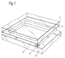
- the cell is filled by applying a vacuum to an aperture (not shown) through one of the glass sheets in one corner of the area enclosed by the perimeter seal so as to causethe liquid crystal medium to enter the cell by way of another aperture (not shown) located in the diagonally opposite corner. (Subsequent to the filling operation the two apertures are sealed.)
- the filling operation is carried out with the filling material heated into its nematic or isotropic phase so as to reduce its viscosity to a suitably low value.
- the basic construction of the cell is similar to that of for instance a conventional twisted nematic, except of course for the parallel alignment of the rubbing directions.
- the thickness of the perimeter seal 13, and hence of the liquid crystal layer is between 1.5 and 3 um, but thinner or thicker layer thicknesses may be required to suit particular applications.
- a preferred thickness is 2um.
- a suitable material for the filling is the smectic C eutectic marketed by BDH of Poole in Dorset under the designation of SCE 3. This material, which exhibits negative dielectric anistropy at least over the frequency range from 1kHz to 40kHz, passes through the smectic A phase on cooling into the smectic C phase from the isotropic phase.
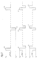
- the positive-going strobe pulse 23 will co-operate with a data 'l' pulse to produced a stimulus of magnitude V S +V D , and thus is capable of being used to set selected pixels from a 'O' state into a 'l' state. It is not capable however of being used to set pixels from a 'l' state into a 'O' state because with neither significance of data pulse will it produce a stimulus of -(V S +V D ).
- a negative-going strobe pulse 24 can set 'l' state pixels into the 'O' state but not 'O' state pixels into the 'l' state. For this reason the addressing is generally operated with the polarity of the strobe pulse being reversed with each refreshing of the cell.
- the data stream is found, under appropriate conditions to provide a sufficient alternating voltage stimulus to the pixels between consecutive refreshings to prevent any appreciable relaxation effects without having to have recourse to any separate signal for stabilisation purposes.
- the efficacy of the data stream in providing this stabilisation is progressively reduced until the point is reached where separate stabilisation at a frequency greater than the fundamental frequency of the data stream does become necessary.
Landscapes
- Physics & Mathematics (AREA)
- Nonlinear Science (AREA)
- Chemical & Material Sciences (AREA)
- Crystallography & Structural Chemistry (AREA)
- General Physics & Mathematics (AREA)
- Engineering & Computer Science (AREA)
- Optics & Photonics (AREA)
- Mathematical Physics (AREA)
- Computer Hardware Design (AREA)
- Theoretical Computer Science (AREA)
- Liquid Crystal (AREA)
- Liquid Crystal Display Device Control (AREA)
- Liquid Crystal Substances (AREA)
Priority Applications (1)
| Application Number | Priority Date | Filing Date | Title |
|---|---|---|---|
| AT88305826T ATE83577T1 (de) | 1987-07-18 | 1988-06-27 | Adressierung von fluessigkristallzellen. |
Applications Claiming Priority (3)
| Application Number | Priority Date | Filing Date | Title |
|---|---|---|---|
| GB8716992A GB2207272B (en) | 1987-07-18 | 1987-07-18 | Addressing liquid crystal cells |
| GB8716992 | 1987-07-18 | ||
| CA000603901A CA1333506C (fr) | 1987-07-18 | 1989-06-26 | Adressage de cellules a cristaux liquides |
Publications (2)
| Publication Number | Publication Date |
|---|---|
| EP0303343A1 true EP0303343A1 (fr) | 1989-02-15 |
| EP0303343B1 EP0303343B1 (fr) | 1992-12-16 |
Family
ID=25672838
Family Applications (1)
| Application Number | Title | Priority Date | Filing Date |
|---|---|---|---|
| EP88305826A Expired - Lifetime EP0303343B1 (fr) | 1987-07-18 | 1988-06-27 | Adressage de cellules à cristaux liquides |
Country Status (8)
| Country | Link |
|---|---|
| US (1) | US4917469A (fr) |
| EP (1) | EP0303343B1 (fr) |
| JP (1) | JP2633312B2 (fr) |
| KR (1) | KR0136798B1 (fr) |
| AT (1) | ATE83577T1 (fr) |
| CA (1) | CA1333506C (fr) |
| DE (1) | DE3876713T2 (fr) |
| GB (1) | GB2207272B (fr) |
Cited By (5)
| Publication number | Priority date | Publication date | Assignee | Title |
|---|---|---|---|---|
| EP0438093A3 (en) * | 1990-01-16 | 1992-02-05 | Honeywell Inc. | Apparatus and method for temperature compensation of liquid crystal displays |
| FR2673027A1 (fr) * | 1991-02-20 | 1992-08-21 | Asahi Optical Co Ltd | Dispositif d'affichage a cristal liquide. |
| EP0450640A3 (en) * | 1990-04-06 | 1992-11-19 | Canon Kabushiki Kaisha | Display apparatus |
| WO1995024715A1 (fr) * | 1994-03-07 | 1995-09-14 | The Secretary Of State For Defence In Her Britannic Majesty's Government Of The United Kingdom Of Great Britain And Northern Ireland | Compensation en temperature de dispositifs d'affichage a cristaux liquides ferroelectriques |
| GB2301450A (en) * | 1994-03-07 | 1996-12-04 | Secr Defence | Temperature compensation of ferroelectric liquid crystal displays |
Families Citing this family (32)
| Publication number | Priority date | Publication date | Assignee | Title |
|---|---|---|---|---|
| GB8726996D0 (en) * | 1987-11-18 | 1987-12-23 | Secr Defence | Multiplex addressing of ferro-electric liquid crystal displays |
| US5117224A (en) * | 1988-02-16 | 1992-05-26 | Casio Computer, Ltd. | Color liquid crystal display apparatus |
| GB8808812D0 (en) * | 1988-04-14 | 1988-05-18 | Emi Plc Thorn | Display device |
| US5029982A (en) * | 1989-09-11 | 1991-07-09 | Tandy Corporation | LCD contrast adjustment system |
| US5132825A (en) * | 1989-10-18 | 1992-07-21 | Asahi Kogaku Kogyo Kabushiki Kaisha | Image processing apparatus having control means for adjusting the color temperature of the displayed image |
| US5196955A (en) * | 1990-05-24 | 1993-03-23 | Semiconductor Energy Laboratory Co., Ltd. | Ferroelectric liquid crystal optical device with viscosity not more than 30000 cps |
| IT1240381B (it) * | 1990-07-06 | 1993-12-10 | Seleco Spa | Circuito generatore di segnali di pilotaggio per display |
| US5798814A (en) * | 1990-08-28 | 1998-08-25 | Semiconductor Energy Laboratory Co., Ltd. | Method of driving a ferroelectric liquid crystal optical device |
| JP2990297B2 (ja) * | 1990-09-10 | 1999-12-13 | セイコーインスツルメンツ株式会社 | 液晶ライトバルブ装置及び液晶ライトバルブの駆動方法 |
| NL9002516A (nl) * | 1990-11-19 | 1992-06-16 | Philips Nv | Weergeefinrichting en werkwijze ter vervaardiging daarvan. |
| US6320568B1 (en) * | 1990-12-31 | 2001-11-20 | Kopin Corporation | Control system for display panels |
| DE69319943T2 (de) * | 1992-02-28 | 1999-02-11 | Canon K.K., Tokio/Tokyo | Flüssigkristallanzeigegerät |
| DE4221784A1 (de) * | 1992-07-03 | 1994-01-05 | Hoechst Ag | Elektrische Adressierung von ferroelektrischen Flüssigkristalldisplays |
| US6115021A (en) * | 1994-07-04 | 2000-09-05 | Sharp Kabushiki Kaisha | Method and apparatus for driving a liquid crystal panel using a ferroelectric liquid crystal material having a negative dielectric anisotropy |
| GB2293906A (en) * | 1994-10-03 | 1996-04-10 | Sharp Kk | Liquid crystal display |
| JPH0980388A (ja) * | 1995-09-11 | 1997-03-28 | Denso Corp | マトリクス型液晶表示装置 |
| KR100506958B1 (ko) * | 1995-12-15 | 2005-10-27 | 코닌클리케 필립스 일렉트로닉스 엔.브이. | 액정디스플레이 장치 |
| GB2313224A (en) | 1996-05-17 | 1997-11-19 | Sharp Kk | Ferroelectric liquid crystal device |
| JPH1039772A (ja) * | 1996-07-29 | 1998-02-13 | Mitsubishi Electric Corp | 投写型液晶表示装置 |
| US6545654B2 (en) | 1996-10-31 | 2003-04-08 | Kopin Corporation | Microdisplay for portable communication systems |
| US6552704B2 (en) | 1997-10-31 | 2003-04-22 | Kopin Corporation | Color display with thin gap liquid crystal |
| US6476784B2 (en) | 1997-10-31 | 2002-11-05 | Kopin Corporation | Portable display system with memory card reader |
| US6909419B2 (en) * | 1997-10-31 | 2005-06-21 | Kopin Corporation | Portable microdisplay system |
| JP2000132145A (ja) * | 1998-10-28 | 2000-05-12 | Alps Electric Co Ltd | 画像表示装置 |
| US6999057B2 (en) * | 2000-02-22 | 2006-02-14 | Kopin Corporation | Timing of fields of video |
| KR100523591B1 (ko) * | 2002-04-09 | 2005-10-26 | 이근홍 | 희토류 금속을 이용한 복합산화물 전극 및 그 제조방법 |
| KR20030095012A (ko) * | 2002-06-11 | 2003-12-18 | 이수테크 주식회사 | 전해조 전극 및 그를 제조하기 위한 제조방법 |
| KR20030095013A (ko) * | 2002-06-11 | 2003-12-18 | 이수테크 주식회사 | 전해조 전극 및 그를 제조하기 위한 제조방법 |
| JP5105694B2 (ja) * | 2003-12-24 | 2012-12-26 | 株式会社半導体エネルギー研究所 | 表示装置及び電子機器 |
| KR100627387B1 (ko) * | 2004-06-29 | 2006-09-21 | 삼성에스디아이 주식회사 | 액정표시장치 및 그의 구동방법 |
| KR100599756B1 (ko) * | 2004-06-29 | 2006-07-12 | 삼성에스디아이 주식회사 | 액정표시장치 및 그의 구동방법 |
| KR102305334B1 (ko) * | 2019-10-04 | 2021-09-28 | 주식회사 웨스코일렉트로드 | 아연도금장치의 양극판 |
Citations (6)
| Publication number | Priority date | Publication date | Assignee | Title |
|---|---|---|---|---|
| DE2316863B2 (de) * | 1972-04-06 | 1977-02-24 | Matsushita Electric Industrial Co., Ltd., Kadoma, Osaka (Japan) | Verfahren zum betrieb eines fluessigkristall-sichtgeraets |
| US4100540A (en) * | 1975-11-18 | 1978-07-11 | Citizen Watch Co., Ltd. | Method of driving liquid crystal matrix display device to obtain maximum contrast and reduce power consumption |
| US4242679A (en) * | 1977-09-13 | 1980-12-30 | Kabushiki Kaisha Suwa Seikosha | Liquid crystal display mechanism |
| FR2546324A1 (fr) * | 1983-05-17 | 1984-11-23 | Thomson Csf | Dispositif de visualisation a memoire entretenue |
| GB2173629A (en) * | 1986-04-01 | 1986-10-15 | Stc Plc | Addressing liquid crystal cells |
| FR2581209A1 (fr) * | 1985-04-26 | 1986-10-31 | Canon Kk | Dispositif optique a cristal liquide |
Family Cites Families (6)
| Publication number | Priority date | Publication date | Assignee | Title |
|---|---|---|---|---|
| US4045791A (en) * | 1972-04-06 | 1977-08-30 | Matsushita Electric Industrial Co., Ltd. | Apparatus for driving liquid crystal display device wherein the signal applied thereto is varied in accordance with the temperature of the device |
| JPS58186796A (ja) * | 1982-04-26 | 1983-10-31 | 社団法人日本電子工業振興協会 | 液晶表示装置およびその駆動方法 |
| FR2541807B1 (fr) * | 1983-02-24 | 1985-06-07 | Commissariat Energie Atomique | Procede de commande sequentielle d'un imageur matriciel utilisant l'effet de transition de phase cholesterique-nematique d'un cristal liquide |
| GB2173337B (en) * | 1985-04-03 | 1989-01-11 | Stc Plc | Addressing liquid crystal cells |
| GB2173336B (en) * | 1985-04-03 | 1988-04-27 | Stc Plc | Addressing liquid crystal cells |
| JPS61249024A (ja) * | 1985-04-26 | 1986-11-06 | Canon Inc | 液晶装置 |
-
1987
- 1987-07-18 GB GB8716992A patent/GB2207272B/en not_active Expired - Lifetime
-
1988
- 1988-06-27 DE DE8888305826T patent/DE3876713T2/de not_active Expired - Fee Related
- 1988-06-27 AT AT88305826T patent/ATE83577T1/de not_active IP Right Cessation
- 1988-06-27 EP EP88305826A patent/EP0303343B1/fr not_active Expired - Lifetime
- 1988-07-01 US US07/214,532 patent/US4917469A/en not_active Expired - Lifetime
- 1988-07-14 JP JP63176186A patent/JP2633312B2/ja not_active Expired - Fee Related
- 1988-07-18 KR KR1019880009006A patent/KR0136798B1/ko not_active Expired - Fee Related
-
1989
- 1989-06-26 CA CA000603901A patent/CA1333506C/fr not_active Expired - Fee Related
Patent Citations (6)
| Publication number | Priority date | Publication date | Assignee | Title |
|---|---|---|---|---|
| DE2316863B2 (de) * | 1972-04-06 | 1977-02-24 | Matsushita Electric Industrial Co., Ltd., Kadoma, Osaka (Japan) | Verfahren zum betrieb eines fluessigkristall-sichtgeraets |
| US4100540A (en) * | 1975-11-18 | 1978-07-11 | Citizen Watch Co., Ltd. | Method of driving liquid crystal matrix display device to obtain maximum contrast and reduce power consumption |
| US4242679A (en) * | 1977-09-13 | 1980-12-30 | Kabushiki Kaisha Suwa Seikosha | Liquid crystal display mechanism |
| FR2546324A1 (fr) * | 1983-05-17 | 1984-11-23 | Thomson Csf | Dispositif de visualisation a memoire entretenue |
| FR2581209A1 (fr) * | 1985-04-26 | 1986-10-31 | Canon Kk | Dispositif optique a cristal liquide |
| GB2173629A (en) * | 1986-04-01 | 1986-10-15 | Stc Plc | Addressing liquid crystal cells |
Cited By (8)
| Publication number | Priority date | Publication date | Assignee | Title |
|---|---|---|---|---|
| EP0438093A3 (en) * | 1990-01-16 | 1992-02-05 | Honeywell Inc. | Apparatus and method for temperature compensation of liquid crystal displays |
| EP0450640A3 (en) * | 1990-04-06 | 1992-11-19 | Canon Kabushiki Kaisha | Display apparatus |
| US5754153A (en) * | 1990-04-06 | 1998-05-19 | Canon Kabushiki Kaisha | Display apparatus |
| FR2673027A1 (fr) * | 1991-02-20 | 1992-08-21 | Asahi Optical Co Ltd | Dispositif d'affichage a cristal liquide. |
| WO1995024715A1 (fr) * | 1994-03-07 | 1995-09-14 | The Secretary Of State For Defence In Her Britannic Majesty's Government Of The United Kingdom Of Great Britain And Northern Ireland | Compensation en temperature de dispositifs d'affichage a cristaux liquides ferroelectriques |
| GB2301450A (en) * | 1994-03-07 | 1996-12-04 | Secr Defence | Temperature compensation of ferroelectric liquid crystal displays |
| GB2301450B (en) * | 1994-03-07 | 1998-01-14 | Secr Defence | Temperature compensation of ferro-electric liquid crystal displays |
| US5825344A (en) * | 1994-03-07 | 1998-10-20 | The Secretary Of State For Defence In Her Britannic Majesty's Government Of The United Kingdom Of Great Britain And Northern Ireland | Temperature compensation of ferro-electric liquid crystal displays |
Also Published As
| Publication number | Publication date |
|---|---|
| DE3876713D1 (de) | 1993-01-28 |
| CA1333506C (fr) | 1994-12-13 |
| GB8716992D0 (en) | 1987-08-26 |
| DE3876713T2 (de) | 1993-04-22 |
| EP0303343B1 (fr) | 1992-12-16 |
| KR890002701A (ko) | 1989-04-11 |
| GB2207272A (en) | 1989-01-25 |
| ATE83577T1 (de) | 1993-01-15 |
| JP2633312B2 (ja) | 1997-07-23 |
| GB2207272B (en) | 1991-08-14 |
| KR0136798B1 (ko) | 1998-04-28 |
| US4917469A (en) | 1990-04-17 |
| JPS6437536A (en) | 1989-02-08 |
Similar Documents
| Publication | Publication Date | Title |
|---|---|---|
| EP0303343B1 (fr) | Adressage de cellules à cristaux liquides | |
| US4909607A (en) | Addressing liquid crystal cells | |
| EP0197742B1 (fr) | Adressage de cellules à cristaux liquides | |
| US5488388A (en) | Liquid crystal apparatus | |
| US4932759A (en) | Driving method for optical modulation device | |
| JPH0344284B2 (fr) | ||
| JPS62278540A (ja) | 液晶素子、その配向制御法及びその駆動法 | |
| EP0366117A3 (fr) | Dispositif à cristal liquide | |
| US5408246A (en) | Electro-optical modulating apparatus and driving method thereof | |
| US5047757A (en) | Method of addressing a ferroelectric liquid crystal display | |
| US6008787A (en) | Antiferrolectric liquid crystal panel and method for driving same | |
| US5136408A (en) | Liquid crystal apparatus and driving method therefor | |
| EP0342835A1 (fr) | Adressage d'une cellule à cristal liquide | |
| US4927243A (en) | Method and apparatus for driving optical modulation device | |
| EP0899711A2 (fr) | Procédé et appareil pour l'adressage d'un dispositif d'affichage à cristaux liquides | |
| EP0196905A2 (fr) | Adressage de cellules à cristaux liquides | |
| JPH11501134A (ja) | 強誘電性液晶表示装置のマルチプレックスアドレシング | |
| JP2584767B2 (ja) | 液晶装置の駆動法 | |
| KR100279684B1 (ko) | 액정 디바이스 및 액정 디바이스를 어드레싱하는 방법 | |
| EP0247806A2 (fr) | Méthode pour commander un dispositif électro-optique à cristaux liquides ferro-électriques | |
| JPH0695179B2 (ja) | 液晶マトリックス表示パネルの駆動法 | |
| JPH06214215A (ja) | 反強誘電性液晶ディスプレイの駆動方法 | |
| JPH0651280A (ja) | 強誘電性液晶素子の駆動方法 | |
| JPH061311B2 (ja) | 液晶装置 | |
| JPH0651279A (ja) | 強誘電性液晶素子の駆動方法 |
Legal Events
| Date | Code | Title | Description |
|---|---|---|---|
| PUAI | Public reference made under article 153(3) epc to a published international application that has entered the european phase |
Free format text: ORIGINAL CODE: 0009012 |
|
| AK | Designated contracting states |
Kind code of ref document: A1 Designated state(s): AT BE CH DE ES FR IT LI LU NL SE |
|
| 17P | Request for examination filed |
Effective date: 19890424 |
|
| 17Q | First examination report despatched |
Effective date: 19910410 |
|
| RAP1 | Party data changed (applicant data changed or rights of an application transferred) |
Owner name: NORTHERN TELECOM LIMITED |
|
| GRAA | (expected) grant |
Free format text: ORIGINAL CODE: 0009210 |
|
| AK | Designated contracting states |
Kind code of ref document: B1 Designated state(s): AT BE CH DE ES FR IT LI LU NL SE |
|
| PG25 | Lapsed in a contracting state [announced via postgrant information from national office to epo] |
Ref country code: IT Free format text: LAPSE BECAUSE OF FAILURE TO SUBMIT A TRANSLATION OF THE DESCRIPTION OR TO PAY THE FEE WITHIN THE PRE;WARNING: LAPSES OF ITALIAN PATENTS WITH EFFECTIVE DATE BEFORE 2007 MAY HAVE OCCURRED AT ANY TIME BEFORE 2007. THE CORRECT EFFECTIVE DATE MAY BE DIFFERENT FROM THE ONE RECORDED.SCRIBED TIME-LIMIT Effective date: 19921216 Ref country code: ES Free format text: THE PATENT HAS BEEN ANNULLED BY A DECISION OF A NATIONAL AUTHORITY Effective date: 19921216 Ref country code: BE Effective date: 19921216 Ref country code: CH Effective date: 19921216 Ref country code: LI Effective date: 19921216 Ref country code: AT Effective date: 19921216 Ref country code: SE Effective date: 19921216 |
|
| REF | Corresponds to: |
Ref document number: 83577 Country of ref document: AT Date of ref document: 19930115 Kind code of ref document: T |
|
| ET | Fr: translation filed | ||
| REF | Corresponds to: |
Ref document number: 3876713 Country of ref document: DE Date of ref document: 19930128 |
|
| REG | Reference to a national code |
Ref country code: CH Ref legal event code: PL |
|
| PG25 | Lapsed in a contracting state [announced via postgrant information from national office to epo] |
Ref country code: LU Free format text: LAPSE BECAUSE OF NON-PAYMENT OF DUE FEES Effective date: 19930630 |
|
| PLBE | No opposition filed within time limit |
Free format text: ORIGINAL CODE: 0009261 |
|
| STAA | Information on the status of an ep patent application or granted ep patent |
Free format text: STATUS: NO OPPOSITION FILED WITHIN TIME LIMIT |
|
| 26N | No opposition filed | ||
| NLV4 | Nl: lapsed or anulled due to non-payment of the annual fee |
Effective date: 19960101 |
|
| NLXE | Nl: other communications concerning ep-patents (part 3 heading xe) |
Free format text: A REQUEST FOR RESTORATION TO THE PRIOR STATE HAS BEEN FILED ON 960626 |
|
| NLXE | Nl: other communications concerning ep-patents (part 3 heading xe) |
Free format text: THE REQUEST FOR RESTORATION TO THE PRIOR STATE AS PROVIDED FOR IN ART.17A OF THE PATENTS ACT HAS BEEN GRANTED;THE RESTORATION OF THE PATENT HAS BEEN ENTERED IN THE PATENT REGISTER |
|
| NLT1 | Nl: modifications of names registered in virtue of documents presented to the patent office pursuant to art. 16 a, paragraph 1 |
Owner name: NORTEL NETWORKS LIMITED;NORTHERN TELECOM LIMITED |
|
| REG | Reference to a national code |
Ref country code: FR Ref legal event code: CD |
|
| NLS | Nl: assignments of ep-patents |
Owner name: CRL OPTO LIMITED, |
|
| PGFP | Annual fee paid to national office [announced via postgrant information from national office to epo] |
Ref country code: NL Payment date: 20060530 Year of fee payment: 19 |
|
| PGFP | Annual fee paid to national office [announced via postgrant information from national office to epo] |
Ref country code: FR Payment date: 20060605 Year of fee payment: 19 |
|
| PGFP | Annual fee paid to national office [announced via postgrant information from national office to epo] |
Ref country code: DE Payment date: 20060630 Year of fee payment: 19 |
|
| NLV4 | Nl: lapsed or anulled due to non-payment of the annual fee |
Effective date: 20080101 |
|
| REG | Reference to a national code |
Ref country code: FR Ref legal event code: ST Effective date: 20080229 |
|
| PG25 | Lapsed in a contracting state [announced via postgrant information from national office to epo] |
Ref country code: DE Free format text: LAPSE BECAUSE OF NON-PAYMENT OF DUE FEES Effective date: 20080101 Ref country code: NL Free format text: LAPSE BECAUSE OF NON-PAYMENT OF DUE FEES Effective date: 20080101 |
|
| PG25 | Lapsed in a contracting state [announced via postgrant information from national office to epo] |
Ref country code: FR Free format text: LAPSE BECAUSE OF NON-PAYMENT OF DUE FEES Effective date: 20070702 |