EP0303397A1 - Signalbehandlungsschaltung - Google Patents
Signalbehandlungsschaltung Download PDFInfo
- Publication number
- EP0303397A1 EP0303397A1 EP88307188A EP88307188A EP0303397A1 EP 0303397 A1 EP0303397 A1 EP 0303397A1 EP 88307188 A EP88307188 A EP 88307188A EP 88307188 A EP88307188 A EP 88307188A EP 0303397 A1 EP0303397 A1 EP 0303397A1
- Authority
- EP
- European Patent Office
- Prior art keywords
- transistor
- integrator
- voltage
- component
- capacitor
- Prior art date
- Legal status (The legal status is an assumption and is not a legal conclusion. Google has not performed a legal analysis and makes no representation as to the accuracy of the status listed.)
- Withdrawn
Links
- 239000003990 capacitor Substances 0.000 claims abstract description 38
- 239000000306 component Substances 0.000 claims description 23
- 238000002485 combustion reaction Methods 0.000 abstract description 3
- 230000010354 integration Effects 0.000 description 5
- 230000001172 regenerating effect Effects 0.000 description 4
- 230000000694 effects Effects 0.000 description 2
- 238000000034 method Methods 0.000 description 2
- 230000003139 buffering effect Effects 0.000 description 1
- 230000001276 controlling effect Effects 0.000 description 1
- 238000010586 diagram Methods 0.000 description 1
- 230000005284 excitation Effects 0.000 description 1
- 230000004907 flux Effects 0.000 description 1
- 230000036039 immunity Effects 0.000 description 1
- 238000005259 measurement Methods 0.000 description 1
- 230000010355 oscillation Effects 0.000 description 1
- 230000003071 parasitic effect Effects 0.000 description 1
- 230000000630 rising effect Effects 0.000 description 1
- 229920006395 saturated elastomer Polymers 0.000 description 1
- 238000004804 winding Methods 0.000 description 1
Images
Classifications
-
- F—MECHANICAL ENGINEERING; LIGHTING; HEATING; WEAPONS; BLASTING
- F02—COMBUSTION ENGINES; HOT-GAS OR COMBUSTION-PRODUCT ENGINE PLANTS
- F02P—IGNITION, OTHER THAN COMPRESSION IGNITION, FOR INTERNAL-COMBUSTION ENGINES; TESTING OF IGNITION TIMING IN COMPRESSION-IGNITION ENGINES
- F02P3/00—Other installations
- F02P3/02—Other installations having inductive energy storage, e.g. arrangements of induction coils
- F02P3/04—Layout of circuits
-
- F—MECHANICAL ENGINEERING; LIGHTING; HEATING; WEAPONS; BLASTING
- F02—COMBUSTION ENGINES; HOT-GAS OR COMBUSTION-PRODUCT ENGINE PLANTS
- F02P—IGNITION, OTHER THAN COMPRESSION IGNITION, FOR INTERNAL-COMBUSTION ENGINES; TESTING OF IGNITION TIMING IN COMPRESSION-IGNITION ENGINES
- F02P7/00—Arrangements of distributors, circuit-makers or -breakers, e.g. of distributor and circuit-breaker combinations or pick-up devices
- F02P7/06—Arrangements of distributors, circuit-makers or -breakers, e.g. of distributor and circuit-breaker combinations or pick-up devices of circuit-makers or -breakers, or pick-up devices adapted to sense particular points of the timing cycle
- F02P7/061—Arrangements of distributors, circuit-makers or -breakers, e.g. of distributor and circuit-breaker combinations or pick-up devices of circuit-makers or -breakers, or pick-up devices adapted to sense particular points of the timing cycle pick-up devices without mechanical contacts
-
- G—PHYSICS
- G01—MEASURING; TESTING
- G01R—MEASURING ELECTRIC VARIABLES; MEASURING MAGNETIC VARIABLES
- G01R19/00—Arrangements for measuring currents or voltages or for indicating presence or sign thereof
- G01R19/175—Indicating the instants of passage of current or voltage through a given value, e.g. passage through zero
-
- H—ELECTRICITY
- H03—ELECTRONIC CIRCUITRY
- H03K—PULSE TECHNIQUE
- H03K3/00—Circuits for generating electric pulses; Monostable, bistable or multistable circuits
- H03K3/02—Generators characterised by the type of circuit or by the means used for producing pulses
- H03K3/023—Generators characterised by the type of circuit or by the means used for producing pulses by the use of differential amplifiers or comparators, with internal or external positive feedback
- H03K3/0233—Bistable circuits
- H03K3/02337—Bistables with hysteresis, e.g. Schmitt trigger
Definitions
- This invention relates to a waveform processing circuit or processor, particularly for signals delivered by a variable reluctance transducer.
- Variable reluctance transducers (usually with permanent magnet excitation) are used to sense predetermined angular positions of rotary shafts, for example a rotor driven by an internal combustion engine in an ignition control system for a vehicle.
- the variable reluctance transducer delivers a sharp zero-crossing emf signal from a winding which links with magnetic flux passing between narrow salient teeth on the rotor and stator. These transducers produce spurious noise which is due either to magnetic interference or to small mechanical disturbances of the transducer assembly.
- a waveform processing circuit which comprises an integrator having an amplifier with a feedback integrating capacitor and means for limiting the voltage across the integrating capacitor prior to a zero-crossing to be detected in an input signal, by interrupting a component of capacitor charging current when the integrator output voltage reaches a first threshold level in one direction and restoring said component of charging current when the integrator output voltage returns to a second threshold level.
- a current source makes a constant current of a given sense available to the integrating capacitor.
- a limiting switch with hysteresis switches this component of charging current away from the capacitor in response to the integrator output voltage reaching its first threshold level in the one direction, and switches the component back to the capacitor in response to the integrator output voltage returning to the second threshold level.
- a second component of charging current, of opposite sense to the interruptible component, is continuously controlled by the amplifier output in accordance with the input signal received by the processor.
- a small component of charging current is provided to the capacitor, of the same sense as the interruptible component, so that the voltage across the capacitor continues to rise during the limiter action.
- the preferred embodiment of waveform processor comprises a comparator with hysteresis to provide a switched output signal from the circuit.
- the comparator switches from a first state to a second state to provide the output signal.
- the comparator switches back to its first state when the integrator output voltage returns to another threshold level.
- the comparator switches to its second state when the limiting switch interrupts the constant component of charging current to the integrator capacitor, and returns to its first state only after this charging component has been restored.
- the switching action of the comparator from its first to its second state is utilised to ensure that interruption of the constant component of charging current occurs abruptly.
- the integrating amplifier comprises an operational amplifier with a virtual earth input node to which the integrator feedback path is connected.
- the integrator feedback can no longer control the virtual earth input node, but an accurate feedback limiter is provided to limit the voltage at the input node under these circumstances to a small excursion of the first polarity away from the virtual earth voltage value.
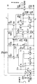
- a waveform processing circuit or processor for signals received at its input VR from a variable reluctance transducer.
- the transducer is mounted adjacent a circumferentially toothed portion of a rotor driven by an internal combustion engine of a vehicle and it is required to derive an output signal each time a tooth of the rotor portion is aligned with the transducer.
- the waveform processor shown in the drawing comprises an integrator having an amplifier with a feedback integrating capacitor C2 and a transistor switch T15 serving as an active output clamp on the integrator and interrupting a charging current normally provided to the integrating capacitor through a constant current source T14, in order to limit the voltage across the capacitor prior to a zero-crossing to be detected in a signal received at an input VR from the transducer.
- the integrator comprises an operational amplifier formed by a longtail pair of transistors T5, T11 having their emitter currents supplied through a resistor R2 and transistor T8 from a 6 volt positive supply rail L.
- Transistors T5 and T11 are of a multi-collector type: transistor T5 has a collector connected through a transistor T6 to ground rail G and another collector connected directly to ground, transistor T11 has two collectors connected through a transistor T10 to ground, whilst transistors T5, T11 each also have two collectors connected to the bases of the transistors T10 and T6 respectively.
- the bases of transistors T6 and T10 are connected to ground through diodes provided by transistors T7 and T9.
- Input buffering and level shifting is provided by input transistors T4 and T13, transistor T13 being of dual-emitter type.
- Transistors T4 and T13 are supplied with their emitter currents through a resistor R3 and a transistor T12 from the supply rail L, have their collectors connected directly to ground and their emitters connected to the bases of the longtail pair transistors T5, T11 respectively.
- Transistor T13 has its base and collector interconnected to act as a diode and the input VR is connected to the base of transistor T4 through a series resistor R1.
- the junction between the collectors of transistors T11 and T10 is connected to the base of a common-emitter transistor stage T17 and the output waveform of the integrator appears at P on the collector of transistor T17.
- a constant current load for transistor T17 is provided by transistor T14 of multi-collector type, having its emitter connected directly to the supply rail L and three collectors connected to the integrator output P through a diode provided by a transistor T16.
- Transistor T14 provides base bias from its other collector for the transistors T8, T12 which have already been described, and also for a further constant current source transistor T18 which will be described below.
- the integrating capacitor C2 of the integrator is connected between the output P of the integrator and the base of input transistor T4.
- the time constant of integration is therefore defined by the feedback capacitor C2 and the series input resistor R1.
- a capacitor C1 is connected between the base of input transistor T4 and ground and serves to reduce the loop gain of the operational amplifier at high frequency in order to ensure stability.
- Two oppositely-poled diodes, formed by transistors T1 and T3, are also connected between the base of input transistor T4 and ground and their purposes will be described below.
- the transistor switch T15 which serves to switch the current made available to the capacitor feedback loop as will be described, is connected to ground in parallel with transistors T16 and T17 and emitter resistor R7 of transistor T17.
- the base of transistor switch T15 is connected to the junction between resistors R4 and R5 connected in series between a diode-strapped collector of transistor T14 and ground.
- the output P of the integrator forms the input to a comparator which comprises a longtail pair of transistors T19 and T20 receiving their emitter currents from the supply rail L through a resistor R8 and the transistor T18 and having their collectors connected to ground through a transistor T21 (acting as a diode) and a transistor T22, respectively.
- Transistor T22 has its base fed from the collector of transistor T19.
- the output P of the integrator is coupled directly to the base of transistor T19 and a reference for the comparator is provided from the junction of resistors R4 and R5 to the base of transistor T20 through a series resistor R9.
- An emitter follower output transistor T24 of the comparator is connected from the base of transistor T20 and through resistors R10 and R11 to ground.
- the base of transistor T24 is connected to the collector of transistor T20 and also through a transistor T23 to ground, the base of transistor T23 being connected to the junction between resistors R10 and R11.
- the processor further comprises an output switching transistor T25 having collector and emitter resistances R12, R13 and its base connected directly to the emitter of transistor T24, the output of the processor being provided at the collector of transistor T25.
- the base of transistor T5 With an input signal to the processor of zero volts, the base of transistor T5 would be at a higher voltage (approximately 20 mV higher in the example shown) than the base of transistor T11, owing to the ratio of the emitter areas of the respective input transistors T4 and T13.
- This offset provides a virtual earth reference voltage of -20 mV for the operational amplifier T5, T11 and ensures that the amplifier output transistor T17 is conducting under quiescent conditions (i.e. input at zero volts).
- transistor T14 forms a current mirror making a constant current available for charging the integrating capacitor C2 through the diode T16 and point P.
- the base voltage thus provided by transistor T14 also determines the constant currents available from transistors T8, T12 and T18.
- Integrator output transistor T17 however passes a controlled value of current to ground from point P.
- the current flowing into capacitor C2 is controlled by transistor T17 tending to hold the base of input transistor T4 at the virtual earth reference level of -20 mV. This current flowing into the capacitor C2 is the difference between the constant current provided by source transistor T14 and the current sunk to ground by transistor T17.
- the capacitor C2 discharges through transistor T17 (now passing more current than is sourced by transistor T14).
- the output P of the integrator provides a signal which is the integral of the input signal.
- the output of the integrator is limited in the negative direction by saturation of transistor T17 and is limited in the positive direction by the clamping action of the transistor switch T15, as will be described below.
- output limiting occurs in either direction, the controlling effect of the virtual earth reference is lost and the base of input transistor T4 tends towards the voltage of the input signal VR. This causes the capacitor C2 to acquire an additional charge which must be removed, when the input signal changes polarity, before the integrator returns to its unsaturated active region.
- this passive integration is minimised during the negative portions of the input signal VR and limited during its positive portions.
- the integrator input voltage is limited in the positive direction by the diode transistor T3 connected between the base of input transistor T4 and ground. Further, the input voltage is limited in the negative direction by an active clamp formed by transistors T5, T11, T6, T7 and T2.
- transistors T5, T11, T6, T7 and T2 are active clamps formed by transistors T5, T11, T6, T7 and T2.
- transistor T6 is saturated due to current in transistors T6 and T7 having a magnitude ratio of approximately 2:1 with balanced conduction in transistors T5 and T11, so that transistor T2 is switched off.
- transistor T5 conducts twice as much current as transistor T11, desaturating transistor T6.
- Transistor T2 therefore starts to conduct and prevents any further fall in the virtual earth input node voltage of the integrator.
- transistor T6 saturates again to switch off transistor T2 and render the input clamp inoperative prior to normal operation of the integrator resuming.
- Diode transistor T1 protects the operational amplifier in the event of excessive negative input signals which cannot be limited by clamping transistor T2.
- the output of the integrator is limited in the negative direction (positive input at VR) by saturation of transistor T17 and is limited in the positive direction (negative input at VR) by the clamping action of the transistor switch T15, controlled in part by the comparator T19, T20.
- the output P of the integrator provides the input to the comparator at the base of transistor T19, the reference for the comparator being provided to the base of transistor T20 through resistor R9 from a clamp reference voltage at the junction of resistors R4 and R5.
- the collector voltage of transistor T22 rises and causes transistor T24 to start conducting when its base reaches 0.6 V (being 1 V be ).
- transistor T24 As the current flowing through transistor T24 increases, regenerative feed-back occurs because the voltage across its collector resistor R9 increases, lowering the reference voltage of the comparator to the base of its transistor T20 and causing further increase in the voltage at the base of transistor T24. This regenerative action continues until the base of transistor T24 reaches 3 V be , when a voltage drop of 1 V be will appear across each of resistors R10 and R11 to switch on transistor T23 and prevent any further rise in the base voltage to transistor T24.
- the comparator exhibits hysteresis and will not switch off transistor T24 until the integrator output has fallen to a lower threshold voltage. This is because with transistor T24 conducting, the comparator has a lower reference voltage applied to the base of transistor T20. Transistor T24 does not saturate and the V be of transistor T23 defines the current through transistor T24 and hence the hysteresis of the comparator.
- the output transistor T25 of the processor starts to conduct when its base voltage reaches 1 V be , which occurs when the base of transistor T24 is at 2 V be . This condition is reached during the regenerative switching-on of transistor T24 and therefore output transistor T25 switches on rapidly, producing a fast and interference-free output signal from the processor. As the integrator output subsequently falls below the lower threshold of the comparator, regenerative action will occur again to switch off transistor T24 and T25, so that both the positive and negative switching edges of the output signal from the processor are fast.
- Switching transistor T15 limits the integrator output in the positive direction as follows. As the integrator output rises towards the comparator reference threshold, the voltages on the bases of transistors T15 and T16 will become equal to cause transistor T15 to conduct and sink the current from transistor T14. The constant current sourced by transistor T14 is no longer available to the integrating capacitor C2. As the comparator also switches at this time, causing transistor T24 to conduct, the voltage at the base of transistor T15 will be reduced thereby ensuring that diode transistor T16 switches off rapidly.
- the hysteresis of the comparator determines the amount of integration of the input waveform which is required after this input changes polarity, before an output signal is produced. This provides the processor with a well-defined noise immunity and signal propagation delay.
- the output clamp of the integrator is operative for a longer time.
- the charging effect of the current component through resistor R6 then becomes significant as it increases the amount of integral required to bring the capacitor voltage down to the level at which switching transistor T15 switches off again and the level at which the comparator switches back. This effect retards the switching edge of the processor output at low engine speeds. But because at higher speeds there is a lag in the transducer output (due to eddy currents), then effectively the rising edge of the output signal from the waveform processor occurs at a constant angle, relative to the adjacent position of the transducer saliencies, over the full speed range.
Landscapes
- Engineering & Computer Science (AREA)
- Chemical & Material Sciences (AREA)
- Combustion & Propulsion (AREA)
- Mechanical Engineering (AREA)
- General Engineering & Computer Science (AREA)
- Physics & Mathematics (AREA)
- General Physics & Mathematics (AREA)
- Manipulation Of Pulses (AREA)
- Dc Digital Transmission (AREA)
Applications Claiming Priority (2)
| Application Number | Priority Date | Filing Date | Title |
|---|---|---|---|
| GB8719157 | 1987-08-13 | ||
| GB878719157A GB8719157D0 (en) | 1987-08-13 | 1987-08-13 | Signal waveform processing circuit |
Publications (1)
| Publication Number | Publication Date |
|---|---|
| EP0303397A1 true EP0303397A1 (de) | 1989-02-15 |
Family
ID=10622241
Family Applications (1)
| Application Number | Title | Priority Date | Filing Date |
|---|---|---|---|
| EP88307188A Withdrawn EP0303397A1 (de) | 1987-08-13 | 1988-08-03 | Signalbehandlungsschaltung |
Country Status (4)
| Country | Link |
|---|---|
| EP (1) | EP0303397A1 (de) |
| JP (1) | JPS6468119A (de) |
| KR (1) | KR890004067A (de) |
| GB (1) | GB8719157D0 (de) |
Cited By (1)
| Publication number | Priority date | Publication date | Assignee | Title |
|---|---|---|---|---|
| DE19507897A1 (de) * | 1995-03-07 | 1996-09-12 | Telefunken Microelectron | Schaltungsanordnung zur Auswertung der Sensorsignale induktiver Sensoren von Kraftfahrzeugen |
Citations (3)
| Publication number | Priority date | Publication date | Assignee | Title |
|---|---|---|---|---|
| US4080574A (en) * | 1974-01-31 | 1978-03-21 | United Kingdom Atomic Energy Authority | Apparatus for providing time reference signals |
| EP0117789A1 (de) * | 1983-02-24 | 1984-09-05 | Automobiles Peugeot | Anordnung zur Auswertung elektrischer Signale erzeugt durch einen Aufnehmer mit variablem magnetischen Widerstand |
| EP0174518A1 (de) * | 1984-08-17 | 1986-03-19 | Fuji Photo Film Co., Ltd. | Nulldurchgangsdetektorschaltung |
-
1987
- 1987-08-13 GB GB878719157A patent/GB8719157D0/en active Pending
-
1988
- 1988-08-03 EP EP88307188A patent/EP0303397A1/de not_active Withdrawn
- 1988-08-12 JP JP63202608A patent/JPS6468119A/ja active Pending
- 1988-08-12 KR KR1019880010292A patent/KR890004067A/ko not_active Withdrawn
Patent Citations (3)
| Publication number | Priority date | Publication date | Assignee | Title |
|---|---|---|---|---|
| US4080574A (en) * | 1974-01-31 | 1978-03-21 | United Kingdom Atomic Energy Authority | Apparatus for providing time reference signals |
| EP0117789A1 (de) * | 1983-02-24 | 1984-09-05 | Automobiles Peugeot | Anordnung zur Auswertung elektrischer Signale erzeugt durch einen Aufnehmer mit variablem magnetischen Widerstand |
| EP0174518A1 (de) * | 1984-08-17 | 1986-03-19 | Fuji Photo Film Co., Ltd. | Nulldurchgangsdetektorschaltung |
Cited By (3)
| Publication number | Priority date | Publication date | Assignee | Title |
|---|---|---|---|---|
| DE19507897A1 (de) * | 1995-03-07 | 1996-09-12 | Telefunken Microelectron | Schaltungsanordnung zur Auswertung der Sensorsignale induktiver Sensoren von Kraftfahrzeugen |
| DE19507897C2 (de) * | 1995-03-07 | 1998-03-12 | Telefunken Microelectron | Schaltungsanordnung zur Erkennung des Nulldurchgangs von Wechselspannungs-Sensorsignalen induktiver Sensoren von Kraftfahrzeugen |
| US5796232A (en) * | 1995-03-07 | 1998-08-18 | Temic Telefunken Microelectronic Gmbh | Circuit configuration for the evaluation of sensor signals of inductive sensors in motor vehicles |
Also Published As
| Publication number | Publication date |
|---|---|
| KR890004067A (ko) | 1989-04-19 |
| JPS6468119A (en) | 1989-03-14 |
| GB8719157D0 (en) | 1987-09-23 |
Similar Documents
| Publication | Publication Date | Title |
|---|---|---|
| US4359649A (en) | Monolithically integrable squarewave pulse generator | |
| GB1139392A (en) | Improvements in and relating to an electrical circuit comprising a constant current pulse generating circuit | |
| US4683409A (en) | Stabilizing arrangement for a stepping motor | |
| US4376914A (en) | Motor control device | |
| US4275703A (en) | Flux control system for a hall generator in an ignition system of an internal combustion engine | |
| GB2064899A (en) | Arrangements for controlling the driving and braking current of a brushless dc motor | |
| US4285323A (en) | Transistorized ignition apparatus for driving ignition coils in an internal combustion engine | |
| US3991730A (en) | Noise immune reset circuit for resetting the integrator of an electronic engine spark timing controller | |
| US3033994A (en) | Resettable delay flop having blocking oscillator whose conduction time is determinedby capactior and clamping means | |
| US4727270A (en) | Noise immune circuit for use with frequency sensor | |
| US3621353A (en) | Phase lock, speed control system | |
| EP0303397A1 (de) | Signalbehandlungsschaltung | |
| US4005476A (en) | Circuit for compensating time errors in a television signal, particularly from a recording instrument | |
| JPH063177B2 (ja) | 誘導発信器用パルス成形器 | |
| US4153864A (en) | Motor speed regulator | |
| US4149116A (en) | Motor speed control system | |
| US4415869A (en) | Sawtooth generator switchable between a free-running state or a synchronizable state | |
| GB2089150A (en) | Rotation stopping apparatus for a motor | |
| US4527121A (en) | Short-circuit-protected evaluation circuit of high stability for variable inductance transducers | |
| US3368134A (en) | Rotatable member speed control system having rotational frequency ambiguity resolver | |
| US4115831A (en) | Velocity detecting apparatus insensitive to noise | |
| US3678356A (en) | Frequency responsive electrical circuit | |
| US4250450A (en) | Detection of engine speed in response to ignition operation | |
| EP0348966B1 (de) | Burst-Torimpulserzeugungsschaltung | |
| US3587001A (en) | Start-stop oscillator control circuit |
Legal Events
| Date | Code | Title | Description |
|---|---|---|---|
| PUAI | Public reference made under article 153(3) epc to a published international application that has entered the european phase |
Free format text: ORIGINAL CODE: 0009012 |
|
| AK | Designated contracting states |
Kind code of ref document: A1 Designated state(s): BE DE FR GB IT SE |
|
| STAA | Information on the status of an ep patent application or granted ep patent |
Free format text: STATUS: THE APPLICATION IS DEEMED TO BE WITHDRAWN |
|
| 18D | Application deemed to be withdrawn |
Effective date: 19890816 |