EP0303435B1 - Transistors bipolaires - Google Patents
Transistors bipolaires Download PDFInfo
- Publication number
- EP0303435B1 EP0303435B1 EP88307335A EP88307335A EP0303435B1 EP 0303435 B1 EP0303435 B1 EP 0303435B1 EP 88307335 A EP88307335 A EP 88307335A EP 88307335 A EP88307335 A EP 88307335A EP 0303435 B1 EP0303435 B1 EP 0303435B1
- Authority
- EP
- European Patent Office
- Prior art keywords
- region
- collector
- contact electrode
- base
- opening
- Prior art date
- Legal status (The legal status is an assumption and is not a legal conclusion. Google has not performed a legal analysis and makes no representation as to the accuracy of the status listed.)
- Expired - Lifetime
Links
Images


Classifications
-
- H—ELECTRICITY
- H10—SEMICONDUCTOR DEVICES; ELECTRIC SOLID-STATE DEVICES NOT OTHERWISE PROVIDED FOR
- H10D—INORGANIC ELECTRIC SEMICONDUCTOR DEVICES
- H10D64/00—Electrodes of devices having potential barriers
- H10D64/20—Electrodes characterised by their shapes, relative sizes or dispositions
- H10D64/23—Electrodes carrying the current to be rectified, amplified, oscillated or switched, e.g. sources, drains, anodes or cathodes
- H10D64/231—Emitter or collector electrodes for bipolar transistors
-
- H—ELECTRICITY
- H10—SEMICONDUCTOR DEVICES; ELECTRIC SOLID-STATE DEVICES NOT OTHERWISE PROVIDED FOR
- H10D—INORGANIC ELECTRIC SEMICONDUCTOR DEVICES
- H10D64/00—Electrodes of devices having potential barriers
- H10D64/20—Electrodes characterised by their shapes, relative sizes or dispositions
- H10D64/27—Electrodes not carrying the current to be rectified, amplified, oscillated or switched, e.g. gates
- H10D64/281—Base electrodes for bipolar transistors
Definitions
- This invention relates to bipolar transistors.
- Figure 6 of the accompanying drawings shows in cross-section such a bipolar transistor in which the base contact electrode is arranged in symmetry with the collector contact electrode.
- An N+ type buried collector region 102 is formed on a semiconductor substrate 101 and an N type epitaxial layer 103 is formed on the collector region 102.
- An isolation region 104 is formed so as to surround the layer 103.
- the N type epitaxial layer 103 serves as a device forming region.
- An N+ type collector contact region 108a and an N type collector contact region 108b for electrical connection with the buried collector region 102, a P type intrinsic base region 109, a graft base region 110 and an emitter region 111 are formed within the N type epitaxial layer 103.
- the collector of the above-described bipolar transistor is connected by way of the buried collector region 102, the N+ type collector contact region 108a and the N type collector contact region 108b to the collector contact electrode 107, while the base of the transistor is connected by way of the intrinsic base region 109 and the graft base region 110 to the base contact electrode 106.
- the spacing or interval between the intrinsic base region 109 and the N type collector region 108b is reduced.
- the P type intrinsic base region 109 and the N type collector contact region 108b can collide with each other, thus resulting in a reduced collector to base breakdown voltage and an increased parasitic capacitance.
- European patent application EP-A-0,144,444 describes an example of a method for manufacturing a bipolar transistor.
- IBM Technical Disclosure Bulletin, volume 24, No. 9, February 1982, pages 4662 - 4664 describes an example of bipolar transistor fabrication using trench isolation.
- United States patent US-A-3,534,234 describes the formation of isolation regions by selective oxidation and the provision of openings through an isolation region.
- French patent application FR-A-2,352,403 also describes the creation of a semiconductor device using trench isolation.
- the abstract of JP-A-60214563 in Patent Abstracts of Japan, vol 10, No 65 (E-388) describes a transistor where polycrystalline layers, each having an As-Doped aperture part and n + type emitter and collector layers formed by heat treatment.
- a bipolar transistor according to the preamble of claim 1 is described in US-A-4252581.
- a bipolar transistor comprising: a monocrystalline semiconductor body on a surface of which an isolation region is formed; a device forming region surrounded by the isolation region; a buried collector region formed in a portion of the device forming region within the semiconductor body; a base region adjacent a portion of a surface of the device forming region; an emitter region adjacent a portion of the surface of the device forming region and surrounded by the base region; a base contact electrode extending from the isolation region to above the device forming region and connected to the base region on the surface of the device forming region; a collector contact electrode spaced from the base contact electrode; and an opening formed through at least a portion of the isolation region; the collector contact electrode being formed over the isolation region and extending through the opening, characterised by: the collector contact electrode being formed from a semiconductor layer which extends over the isolation region and also extends through the opening; a collector contact region contiguous with the buried collector region formed by impurity diffusion from the collector contact electrode for
- a process for manufacturing a bipolar transistor including a buried collector region in a device forming region surrounded by an isolation region of a monocrystalline semiconductor body; and a base region and an emitter region surrounded by the base region on a surface of the device forming region; the process comprising: forming an opening through the isolation by etching off at least a portion of the isolation region; forming a semiconductor layer on the entire surface which extends over the isolation region and extends into the opening; partially removing the semiconductor layer to form a collector contact electrode spaced from a base contact electrode, the collector contact electrode extending through the opening; and forming a collector contact region contiguous to the buried collector region by impurity diffusion from the collector contact electrode, the collector contact region interconnecting the buried collector region and the collector contact electrode; forming a side wall insulating layer where the semiconductor layer was removed; and forming an intrinsic base region by diffusion from a silicon layer between the side walls.
- the process additionally comprises: forming the buried collector region in a monocrystalline semiconductor substrate; producing an epitaxial layer on the monocrystalline semiconductor substrate; forming a mask selectively on the epitaxial layer, which layer acts as the device forming region, and also forming the isolation region surrounding the device forming region by selective oxidation; forming an insulating film over the entire surface; forming the opening in a portion of the device forming region; forming the semiconductor layer on the entire surface which extends over the isolation region and extends into the opening; introducing an impurity into the semiconductor layer so that the layer has different conductivity types as between a first region thereof and a second region thereof which is spaced from the first region and extends through the opening; partially removing the semiconductor layer so that it is divided to form the base and collector contact electrodes corresponding to the first and second regions of different conductivity types and so that the device forming region is exposed; forming the side wall insulating layer where the semiconductor layer was removed; and forming an emitter region contiguous with a surface of the side wall
- a bipolar transistor has a buried collector region, a base region and an emitter region in a device forming region delimited or surrounded by an isolation region.
- the emitter region is isolated by a side wall insulating layer on a major substrate surface.
- the base region is connected to the base contact electrode by way of a graft base region.
- the buried collector region is connected to a collector contact electrode separated from the base contact electrode.
- the collector contact electrode is connected to the buried collector region by way of an opening formed at at least a portion of the isolation region. In a manner distinct from an opening formed previously by selective oxidation, the opening is formed through an isolation region after formation of the isolation region. By making a connection by way of this opening, a larger distance is provided between the base region and the collector contact region to avoid collision between the impurity regions.
- the process for making the bipolar transistor there are steps of forming a buried collector region, a base region and an emitter region in a device forming region surrounded by an isolation region, forming an impurity region contiguous to the buried collector region through an opening formed by etching away at least a portion of the isolation region, and forming a collector contact electrode in said opening.
- Preferred embodiments of the invention described below provide: a bipolar transistor wherein collision between the base region and the collector contact region may be effectively avoided to enable reduction or shrinking of the dimensions of the device to be achieved; and a process for preparing such a bipolar transistor with a higher efficiency.
- a buried collector region, a base region and an emitter region are formed in a device forming region surrounded by an isolation region, an emitter region is formed by the intermediary of a semiconductor layer isolated by a side wall insulating layer, and a base contact electrode and a collector contact electrode are arranged in symmetry with each other.
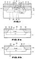
- the bipolar transistor shown in Figure 1 comprises an N+ type buried collector region 12 which is formed on a semiconductor substrate 11.
- An N type epitaxial layer 13 is formed on the buried collector region 12.
- An isolation region 14 is formed adjacent to the N type epitaxial layer 13 by a selective oxidation process.
- the N type epitaxial layer 13 is a device forming region and is surrounded by the isolation region 14.
- a base contact electrode 15, covered by an insulating layer 19, is formed on the surface of the N type epitaxial layer 13, over the isolation region 14, so as partially to contact the surface of the layer 13.
- a collector contact electrode 16 is provided in symmetry with the base contact electrode 15 with respect to an emitter region, and extends over the isolation region 14 and is covered by an insulating layer 19.
- the base contact electrode 15 has a terminal portion that contacts the N type epitaxial layer 13.
- a P+ type graft base region 23 is formed by diffusion of impurities from the base contact electrode 15.
- the graft base region 23 is contiguous with a P type intrinsic base region 20 formed on the major surface of the N type epitaxial layer 13.
- An N+ emitter region 21 is formed within the intrinsic base region 20 so as to face the major surface of the layer 13.
- the emitter region 21 is connected to an emitter electrode (not shown) through a thin polycrystalline silicon layer 18 applied to a space between side walls 17, 17 formed on end surfaces of the base contact electrode 15, collector contact electrode 16 and insulating layer 19.
- the collector contact electrode 16 is not connected to the N type epitaxial layer 13 in the vicinity of the side walls 17, but is connected to the buried collector region 12 through an opening 10 formed in the isolation region 14 towards the side thereof where the collector contact electrode 16 is formed. It is to be noted that the buried collector region 12 and the collector contact electrode 16 are electrically connected to each other through an N+ type collector contact region 22 which is a high concentration impurity region formed in the N type epitaxial layer 13 between the buried collector region 12 and the opening 10 such that, as described later, the characteristics of the bipolar transistor may be improved.
- the opening 10 is formed on a boundary surface which is inclined relative to the major surface and which is disposed between the isolation region 14 and the N type epitaxial layer 13. Although it is known to make an electrical contact or connection at a region previously isolated by the insulating region, the opening 10 is formed in the present embodiment through the isolation region 14. By providing the opening 10 in this manner, the opening 10 is shifted towards the isolation region 14 by a distance equal to l0, for example, as compared to the case shown in Figure 6 in which the collector contact or connection is made in the vicinity of a position corresponding to the side wall 17, similarly to the base contact or connection. Hence, the distance l1 between the intrinsic base region 20 and the collector contact region 22 may be selected to be larger by an amount corresponding to the thus-obtained distance l0.
- the impurity concentration of the collector contact region 22 may be increased in order to lower the collector resistance. This is favourable above all when reduction or shrinking of the dimensions of the device is aimed at.
- the base contact electrode 15 and the collector contact electrode 16 may be arranged completely in symmetry with each other.
- the electrodes 15, 16 may be arranged so as partially to confront each other.
- the position of the opening 10 may be such that a sufficient distance may be obtained between it and the intrinsic base region 20, while the opening 10 may be extended through to the bottom surface of the isolation region 14.
- a PNP type transistor may naturally be employed as the bipolar transistor.
- an N+ type buried collector region 32 is formed on a semiconductor substrate 31, and a N type epitaxial layer 33 is formed or provided on the layer 32.
- An isolation region 34 is formed selectively on the N type epitaxial layer 33, for example by selective oxidation. After formation of the isolation region 34, the region 34 is planarised and the entire surface of the region 34 is covered with a chemical vapour deposition (CVD) SiO2 film or layer 35.
- the surface of the N type epitaxial layer 33 which represents a device forming region, is covered by the CVD SiO2 film 35. Then, a portion of the CVD SiO2 film 35 disposed on the N type epitaxial layer 33 is removed for exposing a portion 36 of the surface of the epitaxial layer.
- an opening 37 is formed by etching away a portion of the isolation region 34.
- the opening 37 may be formed simultaneously with etching of the film 35 to form the exposed surface portion 36 or it may be formed by a separate etching process.
- the opening 37 may, for example, be positioned on the boundary surface between the insulation region 34 and the N type epitaxial layer 33, which is inclined relative to the major surface.
- the area of the buried collector region 32 can be reduced by making the collector contact at this position. However, this positioning is only illustrative and the collector contact may be made at any other position which will ensure a positive separation between the collector contact region and the intrinsic base region to be formed later.
- the opening 37 may be formed so that the buried collector region 32 will exist directly at the bottom of the opening.
- the impurity region contiguous to the buried collector region 32 may be formed on the bottom of the opening 37, such as by ion implantation, after the formation of the opening 37, with the exposed surface portion 36 being masked.
- a polycrystalline silicon layer 38 is formed over the entire surface, as shown in Figure 2c.
- the opening 37 is filled with the polycrystalline silicon layer 38, the polycrystal silicon layer 38 then being contiguous with the N type epitaxial layer 33 at the exposed surface 36.
- the thus-formed polycrystalline silicon layer 38 may be planarised if necessary or if desired.
- N type and P type impurities are selectively introduced by ion implantation into the polycrystalline silicon layer 38.
- an N type impurity for making collector contact is introduced into a part of the polycrystalline silicon layer 38 including the exposed surface portion 36 and the opening 37
- a P type impurity for making base contact is introduced into a part of the polycrystalline silicon layer 38 including the exposed surface portion 36 and not including the opening 37.
- a CVD SiO2 film 39 is deposited over the entire surface of the polycrystalline silicon layer 38.
- a collector contact electrode 41 composed of the part of the polycrystalline silicon layer 38 into which the N type impurity has been introduced is formed in symmetry with a base contact electrode 40 composed of the part of the polycrystalline silicon layer 38 into which the P type impurity has been introduced, with respect to an emitter region which will be formed in the next process step. Since the collector contact electrode 41 also fills the opening 37, collector contact may be made at the opening 37, so that the collector contact electrode need not be extended into contact with the N type epitaxial layer 33 at the exposed surface 36 of the N type epitaxial layer 33.
- the base contact electrode 40 makes contact at a terminal portion 40a thereof with the N type epitaxial layer 33, and the base contact region is formed by impurity diffusion from the terminal portion 40a.
- a CVD SiO2 film is formed and then etched back to form side walls 42, 42.
- a thin polycrystalline silicon layer 47 is then formed between the side walls 42, 42 and a P type impurity is introduced into the layer 47.
- an annealing operation is carried out so that, as shown in Figure 2e, a P type base contact region 43 is formed by diffusion from the terminal portion 40a of the base contact electrode 40, while an intrinsic base region 44 is formed by diffusion from the thin polycrystalline silicon layer 47 into which the impurity has been introduced. Also, in the same step or in a separate step, an N+ type collector contact region 46 interconnecting the buried collector region 32 and the collector contact electrode 41 is formed by impurity diffusion from the collector contact electrode 41 within the opening 37.
- the N type impurity is then introduced to a high concentration into the thin polycrystalline silicon layer 47 and annealing is then carried out so that an emitter region 45 is formed in self-alignment with the intrinsic base region 44.
- the side wall 42 may be of a dual structure, which is highly effective, above all when a projection such as an oxide film exists in the vicinity of the side wall of the collector contact electrode 41. Any type of annealing, such as rapid thermal annealing, may be employed.
- a larger distance may be provided between the intrinsic base region 44 and the collector contact region 46 for reducing the parasitic capacitance and improving the collector to base breakdown voltage.
- the device area may be reduced for promoting integration and reduction or shrinking of the dimensions of the bipolar transistor.
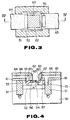
- Figures 3 and 4 illustrate the construction of a bipolar transistor having a trench-shaped isolation region.
- the construction is such that an N+ type buried collector region 52 is formed on a semiconductor substrate 50 and an N type semiconductor crystal region 53 is formed on the N+ type buried collector region 52.
- the N type semiconductor crystal region 53 represents a device forming region which is surrounded by a trench-shaped isolation region 51.
- a base contact electrode 64 is formed on the surface of the N type semiconductor crystal region 53 so as partially to contact said surface and to overlie an insulating layer 61.
- the base contact electrode 64 is covered by an insulating layer 66.
- a collector contact electrode 65 is formed on the insulating layer 61 in symmetry with the base contact electrode 64, and is covered by the insulating layer 66.
- the collector contact electrode 65 is not in surfacial contact with the semiconductor crystal region 53 and has an end surface 62 covered by a side wall 63.
- a portion of the collector contact electrode 65 fills an opening 70 formed in a portion of the trench-shaped isolation region 51.
- the collector contact electrode 65 is connected to an N+ type collector contact region 57 formed in the semiconductor crystal region 53 as a continuation of the N+ type buried collector region 52.
- a base contact region 55 is formed by diffusion on a portion of the semiconductor crystal region 53 contacted by the base contact electrode 64, with the electrode 64 acting as a surface of diffusion.
- An intrinsic base region 54 is formed by diffusion with the side wall 63 acting as a mask and is connected to the base contact region 55.
- An emitter region 56 is similarly formed at the inner side of the intrinsic base region 54, using the same mask.
- a larger distance may be obtained between the intrinsic base region 54 and the collector contact region 57, so that collision between the intrinsic base region 54 and the collector contact region 57 may be avoided so as to reduce the parasitic capacitance and improve the collector to base breakdown voltage.
- a higher impurity concentration of the collector contact region 57 may be realised with a lower collector resistance.
- a further advantage may be obtained when reduction or shrinking of the dimensions of the device components is aimed at.
- Figure 5 illustrates a modification of the bipolar transistor shown in Figures 3 and 4.
- the same references are used in Figure 5 to designate parts or components which are the same as those shown in Figure 4 and the corresponding description will not be repeated.
- the bipolar transistor shown in Figure 5 differs from that shown in Figure 4 as regards the structure of an opening 80 thereof.
- a side wall 81 formed of an insulating material is formed on the lateral wall of the opening 80, the inside of which is filled by a collector contact electrode 65.
- a portion 83 of an N+ type buried collector region 52 is connected to the portion of the collector contact electrode 65 which is defined by the side wall 81.
- isolation between the collector contact region 65 and the intrinsic base region 54 can be additionally ensured by the side wall 81 of the opening 80.
- the base contact electrode and the collector contact electrode need not be arranged completely symmetrically with each other, and that the bipolar transistor may also be a PNP type transistor.
Landscapes
- Bipolar Transistors (AREA)
Claims (8)
- Transistor bipolaire comportant :
un corps semiconducteur monocristallin (11, 31, 50) sur une surface duquel est formée une région d'isolation (14, 34, 51) ;
une région de formation du dispositif (13, 33, 53) entourée par la région d'isolation (14, 34, 51) ;
une région de collecteur enterrée (12, 32, 52, 52) formée dans une partie de la région de formation du dispositif (13, 33, 53) à l'intérieur du corps semiconducteur (11, 31, 50) ;
une région de base (20/23, 44/43, 54/55) adjacente à une partie d'une surface de la région de formation du dispositif (13, 33, 53) ;
une région d'émetteur (21, 45, 56) adjacente à une partie de la surface de la région de formation du dispositif (13, 33, 53) et entourée par la région de base (20/23, 44/43, 54/55) ;
une électrode de contact de base (15, 40, 64) s'étendant depuis la région d'isolation (14, 34, 51) jusqu'au-dessus de la région de formation du dispositif (13, 33, 53) et reliée à la région de base (20/23, 44/43, 54/55) sur la surface de formation du dispositif (13, 33, 53);
une électrode de contact de collecteur (16, 41, 65) espacée de l'électrode de contact de base (15, 40, 64) ; et
une ouverture (10, 37, 70, 80) formée à travers au moins une partie de la région d'isolation (14, 34, 51) ;
l'électrode de contact de collecteur (16, 41, 65) étant formée au-dessus de la région d'isolation (14, 34, 51) et s'étendant à travers l'ouverture (10, 37, 70, 80), caractérisé en ce que :
l'électrode de contact de collecteur (16, 41, 65) est formée à partir d'une couche semiconductrice (38) s'étendant au-dessus de la région d'isolation (14, 34, 51) et s'étendant également à travers l'ouverture (10, 37, 70, 80) ;
une région de contact de collecteur (22, 46, 57, 83)est adjacente à la région de collecteur enterrée (12, 32, 52, 52) formée par diffusion d'impuretés à partir de l'électrode de contact de collecteur pour relier l'électrode de contact de collecteur (16, 41, 65) et la région de collecteur enterrée (12, 32, 52, 52) ;
la région d'émetteur (21, 45, 56) est isolée de l'électrode de contact de base (15, 40, 64) et de l'électrode de contact de collecteur (16, 41, 65) par une couche isolante à paroi latérale (17, 42, 63) ; et
ladite région de base comporte une région de base intrinsèque formée par diffusion depuis une couche de silicium (47) entre les parois latérales. - Transistor bipolaire selon la revendication 1, dans lequel la région de base (20/23, 44/43, 54/55) est formée par la région de base intrinsèque (20, 44, 54) et la région de base dopée (23, 43, 55) reliant la région de base intrinsèque (20, 44, 54) et l'électrode de contact de base (15, 40, 64).
- Transistor bipolaire selon la revendication 1 ou la revendication 2, dans lequel la région d'isolation (14, 34, 51) a été formée par oxydation sélective et l'ouverture (10, 37, 70, 80) est formée à travers la région d'isolation.
- Transistor bipolaire selon la revendication 3, dans lequel l'ouverture (10, 37) est formée dans une surface limite inclinée entre la région d'isolation (14, 34) et la région de formation du dispositif (13, 33).
- Transistor bipolaire selon la revendication 1 ou la revendication 2, dans lequel la région d'isolation (51) est une couche d'isolation sous forme de tranchée et l'ouverture (70, 80) est formée sur un côté de la couche isolante vers la région de formation du dispositif (53).
- Transistor bipolaire selon la revendication 5, dans lequel une couche isolante (81) est formée sur une paroi latérale de l'ouverture (80) et l'ouverture (80) est au contact seulement à la base (82) de celle-ci par la région de collecteur enterrée (52/83).
- Procédé de fabrication d'un transistor bipolaire comprenant :
une région de collecteur enterrée (32) dans une région de formation du dispositif (13) entourée par une région d'isolation (34) d'un corps semiconducteur monocristallin (31) ; et
une région de base (44/43) et une région d'émetteur (45) entourée par la région de base sur une surface de la région de formation du dispositif (33) ;
ledit procédé comportant :
la formation d'une ouverture (37) à travers la région d'isolation par gravure d'au moins une partie de la région d'isolation (34) ;
la formation d'une couche semiconductrice (38) sur toute la surface s'étendant au-dessus de la région d'isolation et s'étendant dans l'ouverture (37) ;
l'élimination partielle de la couche semiconductrice (38) pour former une électrode de contact de collecteur (41) espacée de l'électrode de contact de base (40), l'électrode de contact de collecteur (41) s'étendant à travers l'ouverture (37) ; et
la formation d'une région de contact de collecteur (46) adjacente à la région de collecteur enterrée (32) par diffusion d'impuretés depuis l'électrode de contact de collecteur (41), la région de contact de collecteur (46) reliant la région de collecteur enterrée (32) et l'électrode de contact de collecteur (41) ;
la formation d'une couche isolante à paroi latérale (42) où la couche semiconductrice (38) a été éliminée; et
la formation d'une région de base intrinsèque (44) par diffusion à partir d'une couche de silicium (47) entre les parois latérales. - Procédé de fabrication d'un transistor bipolaire selon la revendication 7, comportant en outre :
la formation d'une région de collecteur enterrée (32) dans un substrat semiconducteur monocristallin (31);
le dépôt d'une couche épitaxiale (33) sur le substrat semiconducteur monocristallin (31) ;
la formation sélective d'un masque sur la couche épitaxiale (33), couche jouant le rôle de région de formation du dispositif, et également la formation de la région d'isolation (34) entourant la région de formation du dispositif (33) par oxydation sélective ;
la formation d'une pellicule isolante (35) sur la surface toute entière ;
la formation de l'ouverture (37) dans une partie de la région de formation du dispositif (33) ;
la formation de la couche semiconductrice (33) sur toute la surface qui s'étend au-dessus de la région d'isolation et s'étend dans l'ouverture (37) ;
l'introduction d'une impureté dans la couche semiconductrice (38), de sorte que la couche présente des types de conductivité différents tels qu'entre une première région de celle-ci et une seconde région de celle-ci qui est espacée de la première région et s'étend à travers l'ouverture (37) ;
l'élimination partielle de la couche semiconductrice (38) de sorte qu'elle est divisée pour former des électrodes de contact de base et de collecteur (40, 41) correspondant aux première et seconde régions de types de conductivité différents et de sorte que la région de formation du dispositif (33) est mise à nu ;
la formation de la couche isolante à paroi latérale (42) où la couche semiconductrice (38) a été éliminée; et
la formation d'une région d'émetteur (45) adjacente à une surface de la couche isolante à paroi latérale (42).
Applications Claiming Priority (2)
| Application Number | Priority Date | Filing Date | Title |
|---|---|---|---|
| JP199006/87 | 1987-08-11 | ||
| JP62199006A JP2615646B2 (ja) | 1987-08-11 | 1987-08-11 | バイポーラトランジスタの製造方法 |
Publications (3)
| Publication Number | Publication Date |
|---|---|
| EP0303435A2 EP0303435A2 (fr) | 1989-02-15 |
| EP0303435A3 EP0303435A3 (en) | 1990-01-03 |
| EP0303435B1 true EP0303435B1 (fr) | 1994-11-02 |
Family
ID=16400538
Family Applications (1)
| Application Number | Title | Priority Date | Filing Date |
|---|---|---|---|
| EP88307335A Expired - Lifetime EP0303435B1 (fr) | 1987-08-11 | 1988-08-08 | Transistors bipolaires |
Country Status (5)
| Country | Link |
|---|---|
| EP (1) | EP0303435B1 (fr) |
| JP (1) | JP2615646B2 (fr) |
| KR (1) | KR0122736B1 (fr) |
| CA (1) | CA1309191C (fr) |
| DE (1) | DE3851991T2 (fr) |
Families Citing this family (9)
| Publication number | Priority date | Publication date | Assignee | Title |
|---|---|---|---|---|
| GB9013926D0 (en) * | 1990-06-22 | 1990-08-15 | Gen Electric Co Plc | A vertical pnp transistor |
| FR2672733B1 (fr) * | 1991-02-13 | 1997-08-22 | France Telecom | Perfectionnement au collecteur d'un transistor bipolaire compatible avec la technologie mos. |
| US5389553A (en) * | 1993-06-30 | 1995-02-14 | National Semiconductor Corporation | Methods for fabrication of transistors |
| JP2708027B2 (ja) * | 1995-10-05 | 1998-02-04 | 日本電気株式会社 | 半導体装置およびその製造方法 |
| US6121102A (en) * | 1997-03-18 | 2000-09-19 | Telfonaktiebolaget Lm Ericsson | Method of electrical connection through an isolation trench to form trench-isolated bipolar devices |
| CA2295990A1 (fr) * | 1997-07-11 | 1999-01-21 | Infineon Technologies Ag | Procede pour la fabrication de composants de circuit integre a usage en hautes frequences |
| EP1228533B1 (fr) * | 2000-07-03 | 2008-09-03 | Nxp B.V. | Procede de fabrication d'un dispositif semi-conducteur a transistor bipolaire |
| EP3214036A1 (fr) * | 2016-03-02 | 2017-09-06 | Anheuser-Busch InBev S.A. | Robinet pour boissons avec tuyau amovible et vanne |
| CN110010677B (zh) * | 2019-04-25 | 2024-02-13 | 江苏新顺微电子股份有限公司 | 一种改善结终端延伸结构三极管可靠性的器件结构及其制造方法 |
Family Cites Families (7)
| Publication number | Priority date | Publication date | Assignee | Title |
|---|---|---|---|---|
| US3534234A (en) * | 1966-12-15 | 1970-10-13 | Texas Instruments Inc | Modified planar process for making semiconductor devices having ultrafine mesa type geometry |
| FR2352403A1 (fr) * | 1976-05-20 | 1977-12-16 | Comp Generale Electricite | Circuit integre rapide |
| US4252581A (en) * | 1979-10-01 | 1981-02-24 | International Business Machines Corporation | Selective epitaxy method for making filamentary pedestal transistor |
| JPS59217364A (ja) * | 1983-05-26 | 1984-12-07 | Sony Corp | 半導体装置の製法 |
| JPS60253267A (ja) * | 1984-05-29 | 1985-12-13 | Toshiba Corp | ヘテロ接合バイポ−ラトランジスタおよびその製造方法 |
| EP0177246B1 (fr) * | 1984-09-29 | 1988-08-17 | Kabushiki Kaisha Toshiba | Transistor bipolaire à hétérojonction et procédé de fabrication |
| JPS61265867A (ja) * | 1985-05-20 | 1986-11-25 | Nec Corp | 半導体装置 |
-
1987
- 1987-08-11 JP JP62199006A patent/JP2615646B2/ja not_active Expired - Fee Related
-
1988
- 1988-07-28 CA CA000573242A patent/CA1309191C/fr not_active Expired - Lifetime
- 1988-08-05 KR KR1019880010002A patent/KR0122736B1/ko not_active Expired - Fee Related
- 1988-08-08 DE DE3851991T patent/DE3851991T2/de not_active Expired - Fee Related
- 1988-08-08 EP EP88307335A patent/EP0303435B1/fr not_active Expired - Lifetime
Non-Patent Citations (1)
| Title |
|---|
| PATENT ABSTRACTS OF JAPAN, vol. 10, no. 65 (E-388), 14 March 1986 ; & JP-A-60214563 * |
Also Published As
| Publication number | Publication date |
|---|---|
| KR890004439A (ko) | 1989-04-22 |
| EP0303435A3 (en) | 1990-01-03 |
| DE3851991T2 (de) | 1995-04-20 |
| JPS6442859A (en) | 1989-02-15 |
| EP0303435A2 (fr) | 1989-02-15 |
| KR0122736B1 (ko) | 1997-11-26 |
| DE3851991D1 (de) | 1994-12-08 |
| CA1309191C (fr) | 1992-10-20 |
| JP2615646B2 (ja) | 1997-06-04 |
Similar Documents
| Publication | Publication Date | Title |
|---|---|---|
| EP0036082B1 (fr) | Procédé autoaligné pour la réalisation d'un transistor bipolaire à haute performance | |
| US4641416A (en) | Method of making an integrated circuit structure with self-aligned oxidation to isolate extrinsic base from emitter | |
| US4481706A (en) | Process for manufacturing integrated bi-polar transistors of very small dimensions | |
| US4994400A (en) | Method of fabricating a semiconductor device using a tri-layer structure and conductive sidewalls | |
| EP0083816B1 (fr) | Dispositif semi-conducteur comprenant une configuration d'interconnexion | |
| US5187554A (en) | Bipolar transistor | |
| EP0310087B1 (fr) | Dispositif semi-conducteur ayant un transistor bipolaire avec rainure | |
| EP0162774B1 (fr) | Améliorations dans les procédés de fabrication d'une puce à circuit intégré et d'une puce réalisée selon ces procédés | |
| EP0372476B1 (fr) | Dispositif semi-conducteur ayant une capacité parasite réduite et méthode pour sa fabrication | |
| US4709469A (en) | Method of making a bipolar transistor with polycrystalline contacts | |
| US4992843A (en) | Collector contact of an integrated bipolar transistor | |
| US5039624A (en) | Method of manufacturing a bipolar transistor | |
| EP0058124A1 (fr) | Matrice de diodes Schottky en silicium polycristallin et procédé de fabrication | |
| US20030193077A1 (en) | Bipolar transistor and method of fabricating the same | |
| EP0303435B1 (fr) | Transistors bipolaires | |
| EP0288691A1 (fr) | Structure à transistor bipolaire avec un dispositif et une isolation auto-alignés et son procédé de fabrication | |
| US5057443A (en) | Method for fabricating a trench bipolar transistor | |
| JPH09181089A (ja) | 超自己整列バイポーラトランジスタの製造方法 | |
| KR100292905B1 (ko) | 절연체상의반도체기판상의바이폴라트랜지스터및그제조방법 | |
| EP0147249B1 (fr) | Procédé pour fabriquer des structures à transistor comportant des jonctions délimitées par des couches isolantes et structures résultantes | |
| JP2501806B2 (ja) | 壁スペ−サを有するバイポ−ラ半導体装置の製造方法 | |
| US5574306A (en) | Lateral bipolar transistor and FET | |
| JPS587862A (ja) | バイポ−ラ型トランジスタ−構造体及びその製造方法 | |
| US5747871A (en) | Bipolar transistor having a self-aligned base electrode and method for manufacturing the same | |
| EP0724298B1 (fr) | Dispositif semi-conducteur avec transistor bipolaire et son procédé de fabrication |
Legal Events
| Date | Code | Title | Description |
|---|---|---|---|
| PUAI | Public reference made under article 153(3) epc to a published international application that has entered the european phase |
Free format text: ORIGINAL CODE: 0009012 |
|
| AK | Designated contracting states |
Kind code of ref document: A2 Designated state(s): DE FR GB NL |
|
| PUAL | Search report despatched |
Free format text: ORIGINAL CODE: 0009013 |
|
| AK | Designated contracting states |
Kind code of ref document: A3 Designated state(s): DE FR GB NL |
|
| 17P | Request for examination filed |
Effective date: 19900530 |
|
| 17Q | First examination report despatched |
Effective date: 19921001 |
|
| GRAA | (expected) grant |
Free format text: ORIGINAL CODE: 0009210 |
|
| AK | Designated contracting states |
Kind code of ref document: B1 Designated state(s): DE FR GB NL |
|
| REF | Corresponds to: |
Ref document number: 3851991 Country of ref document: DE Date of ref document: 19941208 |
|
| ET | Fr: translation filed | ||
| PLBE | No opposition filed within time limit |
Free format text: ORIGINAL CODE: 0009261 |
|
| STAA | Information on the status of an ep patent application or granted ep patent |
Free format text: STATUS: NO OPPOSITION FILED WITHIN TIME LIMIT |
|
| 26N | No opposition filed | ||
| PGFP | Annual fee paid to national office [announced via postgrant information from national office to epo] |
Ref country code: DE Payment date: 20010730 Year of fee payment: 14 |
|
| PGFP | Annual fee paid to national office [announced via postgrant information from national office to epo] |
Ref country code: GB Payment date: 20010808 Year of fee payment: 14 |
|
| PGFP | Annual fee paid to national office [announced via postgrant information from national office to epo] |
Ref country code: FR Payment date: 20010810 Year of fee payment: 14 |
|
| PGFP | Annual fee paid to national office [announced via postgrant information from national office to epo] |
Ref country code: NL Payment date: 20010830 Year of fee payment: 14 |
|
| REG | Reference to a national code |
Ref country code: GB Ref legal event code: IF02 |
|
| PG25 | Lapsed in a contracting state [announced via postgrant information from national office to epo] |
Ref country code: GB Free format text: LAPSE BECAUSE OF NON-PAYMENT OF DUE FEES Effective date: 20020808 |
|
| PG25 | Lapsed in a contracting state [announced via postgrant information from national office to epo] |
Ref country code: NL Free format text: LAPSE BECAUSE OF NON-PAYMENT OF DUE FEES Effective date: 20030301 Ref country code: DE Free format text: LAPSE BECAUSE OF NON-PAYMENT OF DUE FEES Effective date: 20030301 |
|
| GBPC | Gb: european patent ceased through non-payment of renewal fee |
Effective date: 20020808 |
|
| PG25 | Lapsed in a contracting state [announced via postgrant information from national office to epo] |
Ref country code: FR Free format text: LAPSE BECAUSE OF NON-PAYMENT OF DUE FEES Effective date: 20030430 |
|
| NLV4 | Nl: lapsed or anulled due to non-payment of the annual fee |
Effective date: 20030301 |
|
| REG | Reference to a national code |
Ref country code: FR Ref legal event code: ST |