EP0304064A2 - Système de connexion à plusieurs étages - Google Patents
Système de connexion à plusieurs étages Download PDFInfo
- Publication number
- EP0304064A2 EP0304064A2 EP88113451A EP88113451A EP0304064A2 EP 0304064 A2 EP0304064 A2 EP 0304064A2 EP 88113451 A EP88113451 A EP 88113451A EP 88113451 A EP88113451 A EP 88113451A EP 0304064 A2 EP0304064 A2 EP 0304064A2
- Authority
- EP
- European Patent Office
- Prior art keywords
- binary
- optical
- couplers
- coupler
- switching
- Prior art date
- Legal status (The legal status is an assumption and is not a legal conclusion. Google has not performed a legal analysis and makes no representation as to the accuracy of the status listed.)
- Granted
Links
Images
Classifications
-
- H—ELECTRICITY
- H04—ELECTRIC COMMUNICATION TECHNIQUE
- H04Q—SELECTING
- H04Q11/00—Selecting arrangements for multiplex systems
- H04Q11/0001—Selecting arrangements for multiplex systems using optical switching
- H04Q11/0005—Switch and router aspects
-
- H—ELECTRICITY
- H04—ELECTRIC COMMUNICATION TECHNIQUE
- H04Q—SELECTING
- H04Q11/00—Selecting arrangements for multiplex systems
- H04Q11/0001—Selecting arrangements for multiplex systems using optical switching
- H04Q11/0005—Switch and router aspects
- H04Q2011/0052—Interconnection of switches
Definitions
- LWL fiber optic
- two strip waveguides - are narrow thin strips produced by diffusion (e.g. of titanium in lithium niobate) in a substrate and have a larger optical refractive index than the substrate - are very narrow in a coupling area of a certain length, at a distance of typically about 5 ⁇ m, guided side by side so that the optical fields overlap and light energy can be coupled from one strip waveguide to the other strip waveguide;
- 2x2 coupling elements which are only capable of two switching states - namely uncrossed switching and crossed switching - are also referred to as binary couplers in switching technology (DE-PS 2 036 176), controllable electro-optical directional couplers used as 2x2 coupling elements can also be used as optical binary couplers be addressed.
- the object of the invention is to provide a switching network in which, in such a case, no switching network connection is nevertheless connected to another switching network connection.
- the invention relates to a multi-stage coupling arrangement with a plurality of optical binary couplers interconnected symmetrically to the switching center line;
- This coupling arrangement is characterized according to the invention in that each switching matrix connection forms the tip of an individual pyramid of optical binary couplers, each pyramid ending in front of the switching center line, in which each optical binary coupler on the side facing away from the switching center line is unconnected in one of its two optical paths and that is via the switching center is connected to each other on the other side of the binary coupler pyramid in a light-conducting manner such that each switching matrix interconnection path starting from a switching matrix connection or leading to a switching matrix connection contains such an unconnected optical fiber path of an optical binary coupler when all binary couplers are switched through.
- the invention has the advantage of being able to avoid undesired connections of switching matrix connections in a coupling arrangement formed with optical binary couplers in the event of failure of the binary coupler control voltages.
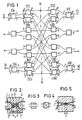
- FIG. 1 shows schematically, in a scope necessary for understanding the invention, an exemplary embodiment of a multi-stage coupling arrangement according to the invention, which is connected to a plurality of optical binary couplers IIA,..., INA; IlJl, ..., INJn; lJlO, ..., nJNO; AlO, ..., ANO is formed; these binary couplers are grouped into switching matrix connection-specific pyramids, the apex of which is formed by the respective switching matrix connection and the base of which lies in front of the switching matrix center line M - M.
- Optical binary couplers are known per se, for example in the form of controllable electro-optical directional couplers (e.g. from the literature references mentioned at the beginning); they are each capable of only two switching states, namely the state of an uncrossed connection, as indicated in FIG. 3, and the state of a crossed connection, as indicated in FIG. 4. 2 schematically shows such an optical binary coupler formed with a controllable electro-optical directional coupler in essential details:
- Two strip waveguides a ′ - i ′ and a ⁇ - i ⁇ are diffused into a substrate, for example lithium niobate; In the actual coupling area having a certain length, the two strip waveguides are closely guided at a distance of typically about 5 ⁇ m, so that light energy can be coupled from one to the other strip waveguide.
- control electrodes E, E ', E ⁇ and O, O', O ⁇ which can be acted upon by a corresponding electrical control voltage from control signal terminals s, so that no overcoupling takes place; the binary coupler is then in the uncrossed state in which, for example, light entering the light guide path a ⁇ exits the light guide path i ⁇ again.
- the state of a cross-connection in which, for example, light entering the light guide path a ⁇ emerges again from the light guide path i ′, there is such an optical binary coupler in the absence of a control voltage, for example due to a supply voltage failure. Accordingly, in order to return to FIG.
- the switching network connection IN is optically connected to the switching network connection 10, and it is, for example, at uncrossed connection of the two binary couplers IlA and 1JNO and crossed connection of the two binary couplers IlJn and ANO the switching network connection Il with the switching network connection NO is connected in a light-conducting manner.
- each optical binary coupler of the individual switching network connection individual pyramids of optical binary couplers on the side applied to the switching network center line M - M is not connected in one of its two light guide paths; Over the switching center line M - M, the binary coupler pyramids are connected in a light-conducting manner to each binary coupler pyramid lying on the other side such that each switching matrix interconnection path starting from a switching matrix connection or leading to a switching matrix connection, with all binary couplers crossed through, connects such an unconnected optical conductor path of an optical binary coupler contains.
- the coupling arrangement sketched in FIG. 1 is a 4-stage 4x4 coupling arrangement with 2-stage coupling field connection-specific binary coupler pyramids.
- the invention is not limited to the realization of the binary couplers with controllable optoelectric directional couplers, which is illustrated in FIG. 2; Rather, the binary couplers can also be implemented differently, for example with so-called Bragg reflectors, as is indicated schematically in FIG. 5:
- an electro-optical crystal for example lithium niobate
- diffusion for example of titanium
- two are under twice the so-called Bragg-Winkel intersecting strip waveguides a '- i ⁇ and a ⁇ - i' are formed, in the intersection of which a finger-shaped electrode structure is provided, which can be acted upon by a corresponding electrical control voltage from control signal terminals s.
- a refractive index grating can be generated in the intersection area due to the electro-optical effect, on which light incident at the Bragg angle is deflected, so that incident light and deflected light enclose the double Bragg angle (see, for example, DE-A 3 025 083, FIG. 1):
- the binary coupler according to FIG. 5 is then in the uncrossed state in which, for example, light entering the light guide path a ⁇ exits the light guide path i ⁇ again.
- the binary coupler is then in the state of crossed connection, in which, for example, light entering the light guide path a ⁇ emerges again from the light guide path i '.
- the unconnected light guide path of the optical binary coupler denoted by a in FIG. 5 can in turn be terminated with a light-absorbing layer Z.
Landscapes
- Engineering & Computer Science (AREA)
- Computer Networks & Wireless Communication (AREA)
- Use Of Switch Circuits For Exchanges And Methods Of Control Of Multiplex Exchanges (AREA)
- Optical Communication System (AREA)
- Optical Integrated Circuits (AREA)
- Data Exchanges In Wide-Area Networks (AREA)
- Small-Scale Networks (AREA)
- Oscillators With Electromechanical Resonators (AREA)
Priority Applications (1)
| Application Number | Priority Date | Filing Date | Title |
|---|---|---|---|
| AT88113451T ATE96598T1 (de) | 1987-08-20 | 1988-08-18 | Mehrstufige koppelanordnung. |
Applications Claiming Priority (2)
| Application Number | Priority Date | Filing Date | Title |
|---|---|---|---|
| DE3727827 | 1987-08-20 | ||
| DE3727827 | 1987-08-20 |
Publications (3)
| Publication Number | Publication Date |
|---|---|
| EP0304064A2 true EP0304064A2 (fr) | 1989-02-22 |
| EP0304064A3 EP0304064A3 (en) | 1990-07-04 |
| EP0304064B1 EP0304064B1 (fr) | 1993-10-27 |
Family
ID=6334147
Family Applications (1)
| Application Number | Title | Priority Date | Filing Date |
|---|---|---|---|
| EP88113451A Expired - Lifetime EP0304064B1 (fr) | 1987-08-20 | 1988-08-18 | Système de connexion à plusieurs étages |
Country Status (9)
| Country | Link |
|---|---|
| US (1) | US5010542A (fr) |
| EP (1) | EP0304064B1 (fr) |
| JP (1) | JPS6490423A (fr) |
| AT (1) | ATE96598T1 (fr) |
| CA (1) | CA1311384C (fr) |
| DE (1) | DE3885198D1 (fr) |
| HU (1) | HU200051B (fr) |
| LU (1) | LU87165A1 (fr) |
| RU (1) | RU1776358C (fr) |
Families Citing this family (13)
| Publication number | Priority date | Publication date | Assignee | Title |
|---|---|---|---|---|
| GB8904281D0 (en) * | 1989-02-24 | 1989-04-12 | British Telecomm | Optical interconnect networks |
| GB8925454D0 (en) * | 1989-11-10 | 1989-12-28 | British Telecomm | Generalised connection network |
| US5311345A (en) * | 1992-09-30 | 1994-05-10 | At&T Bell Laboratories | Free space optical, growable packet switching arrangement |
| JPH07312576A (ja) * | 1994-05-17 | 1995-11-28 | Sumitomo Electric Ind Ltd | 光伝送路の故障検出方式 |
| US5524154A (en) * | 1994-08-31 | 1996-06-04 | At&T Corp. | Hybrid architecture for an optical switching fabric implemented with 1×2 switching devices |
| DE4437325A1 (de) * | 1994-10-19 | 1996-04-25 | Bosch Gmbh Robert | Optischer Schalter und optisches Koppelfeld damit |
| KR0159663B1 (ko) * | 1995-10-28 | 1998-12-01 | 김광호 | 광데이타 전송 이중화를 구현한 광데이타 전송장치 |
| US6236775B1 (en) * | 1998-05-19 | 2001-05-22 | Lynx Photonic Networks Inc. | Integrated optical switch array |
| JP2003529097A (ja) * | 2000-03-27 | 2003-09-30 | リンクス フォトニック ネットワークス インコーポレイテッド | パワーのバランス化を有する光交換システム |
| US6445843B1 (en) * | 2000-12-20 | 2002-09-03 | Lynx Photonic Networks Inc. | Optical switching system with power balancing |
| JP2003199130A (ja) * | 2001-12-27 | 2003-07-11 | Fujitsu Ltd | 光パスクロスコネクト装置及びその切替方法 |
| US8351338B2 (en) * | 2009-03-23 | 2013-01-08 | Jds Uniphase Corporation | Sharing single tester among plurality of active communication links |
| CN103370650B (zh) * | 2011-02-15 | 2016-01-06 | 日本电信电话株式会社 | 波导型光开关 |
Family Cites Families (15)
| Publication number | Priority date | Publication date | Assignee | Title |
|---|---|---|---|---|
| DE582206C (de) * | 1929-01-09 | 1933-08-10 | Siemens & Halske Akt Ges | Schaltungsanordnung fuer Relaiswaehler |
| DE1115775B (de) * | 1960-03-08 | 1961-10-26 | Siemens Ag | Relaiskontaktpyramide fuer Fernmelde-, insbesondere Fernsprechanlagen |
| AT318018B (de) * | 1970-07-21 | 1974-09-25 | Siemens Ag | Koppelanordnung mit einer Mehrzahl von untereinander verbundenen, jeweils nur zwei erste und zwei zweite Leitungen aufweisenden Koppelvielfachen (Binärkopplern) |
| DE2421002C3 (de) * | 1974-04-30 | 1980-07-03 | Siemens Ag, 1000 Berlin Und 8000 Muenchen | Nachrichtenvermittlungssystem |
| US4011543A (en) * | 1976-02-20 | 1977-03-08 | Sperry Rand Corporation | Low crosstalk optical switch |
| DE3025083A1 (de) * | 1980-07-02 | 1982-01-21 | Siemens AG, 1000 Berlin und 8000 München | Planarer elektrooptischer lichtablenker fuer mehrere strahlpositionen |
| DE3230251A1 (de) * | 1981-09-30 | 1984-01-05 | Siemens AG, 1000 Berlin und 8000 München | Als schalter dienender richtungskoppler fuer optische signale und verfahren zur herstellung desselben |
| DE3235266A1 (de) * | 1982-09-23 | 1984-03-29 | Siemens AG, 1000 Berlin und 8000 München | Kopplernetzwerk zum verkoppeln mehrerer teilnehmersender mit mehreren teilnehmerempfaengern |
| GB8333519D0 (en) * | 1983-12-16 | 1984-01-25 | Gen Electric Co Plc | Data signal switching systems |
| DE3423221A1 (de) * | 1984-06-21 | 1984-11-29 | Heinrich-Hertz-Institut für Nachrichtentechnik Berlin GmbH, 1000 Berlin | Optischer sternkoppler mit einer grossen zahl von ein- und ausgaengen |
| SE450173B (sv) * | 1985-08-15 | 1987-06-09 | Ericsson Telefon Ab L M | Polarisationsoberoende elektrooptisk omkopplare |
| US4731878A (en) * | 1985-11-29 | 1988-03-15 | American Telephone And Telegraph Company, At&T Bell Laboratories | Self-routing switch node combining electronic and photonic switching |
| CA1284904C (fr) * | 1986-01-31 | 1991-06-18 | Kazuo Hajikano | Commutateur spatial optique |
| US4787692A (en) * | 1987-03-13 | 1988-11-29 | American Telephone And Telegraph Company At&T Bell Laboratories | Electro optical switch architectures |
| US4807280A (en) * | 1987-09-18 | 1989-02-21 | Pacific Bell | Cross-connect switch |
-
1988
- 1988-03-16 LU LU87165A patent/LU87165A1/de unknown
- 1988-07-29 RU SU884356166A patent/RU1776358C/ru active
- 1988-08-15 JP JP63203689A patent/JPS6490423A/ja active Pending
- 1988-08-15 US US07/232,504 patent/US5010542A/en not_active Expired - Fee Related
- 1988-08-18 EP EP88113451A patent/EP0304064B1/fr not_active Expired - Lifetime
- 1988-08-18 CA CA000575087A patent/CA1311384C/fr not_active Expired - Lifetime
- 1988-08-18 AT AT88113451T patent/ATE96598T1/de active
- 1988-08-18 DE DE88113451T patent/DE3885198D1/de not_active Expired - Fee Related
- 1988-08-19 HU HU884410A patent/HU200051B/hu not_active IP Right Cessation
Also Published As
| Publication number | Publication date |
|---|---|
| EP0304064A3 (en) | 1990-07-04 |
| JPS6490423A (en) | 1989-04-06 |
| CA1311384C (fr) | 1992-12-15 |
| LU87165A1 (de) | 1988-08-23 |
| HU200051B (en) | 1990-03-28 |
| HUT47772A (en) | 1989-03-28 |
| RU1776358C (ru) | 1992-11-15 |
| DE3885198D1 (de) | 1993-12-02 |
| US5010542A (en) | 1991-04-23 |
| EP0304064B1 (fr) | 1993-10-27 |
| ATE96598T1 (de) | 1993-11-15 |
Similar Documents
| Publication | Publication Date | Title |
|---|---|---|
| DE3876434T2 (de) | Verbesserungen in elektro-optischen schalterarchitekturen. | |
| EP0304064B1 (fr) | Système de connexion à plusieurs étages | |
| DE69023489T2 (de) | Optische Koppelvorrichtung. | |
| DE3124488C2 (de) | Elektrooptischer Schalter mit Flüssigkristallmatrixzelle | |
| DE69529626T2 (de) | Optischer wellenleiterkreuzungspunktschalter | |
| DE2400491C2 (de) | Fasernetz für die optoelektronische Übertragung von Daten | |
| DE60023048T2 (de) | Optische Raumkoppelfelder mit Mehrtor-Kopplern | |
| DE69927636T2 (de) | Multiport optischer Zirkulator welcher eine Abbildungslinse und ein korrigierendes optisches Element benutzt | |
| WO1996008932A1 (fr) | Matrice de commutation optique 1xn et nxn arborescente | |
| EP0968452B1 (fr) | Element de commutation optique et agencement de commutation | |
| DE69901650T2 (de) | Optischer Mehrfachkoppler mit Linse | |
| DE3644309A1 (de) | Integrierter optischer schalter | |
| EP0419720B1 (fr) | Système de télécommunication à fibre optique avec un ou plusiers commutateurs optiques situés sur le chemin optique | |
| DE60101369T2 (de) | Optische Schaltmatrix | |
| EP0807357B1 (fr) | PROCEDE DE FONCTIONNEMENT D'UN SYSTEME DE COMMUTATION SPATIALE NxN MULTINIVEAU | |
| EP0587930A1 (fr) | Réseau de commutation optique pour des cellules optiques de communication | |
| EP0968454A1 (fr) | Disjoncteur optique a coupure multiple | |
| LU87901A1 (de) | Passives optisches telekommunikationssystem | |
| DE60127667T2 (de) | Optischer flüssigkristallschalter mit zuverlässiger steuerung | |
| DE102007015766A1 (de) | Lasermodul für Projektoren | |
| DE3618037C1 (en) | Optical component | |
| EP0304065A1 (fr) | Système de télécommunication utilisant un réseau de connexions optiques en étoile | |
| DE3423221A1 (de) | Optischer sternkoppler mit einer grossen zahl von ein- und ausgaengen | |
| EP0453655B1 (fr) | Mélangeur de lumière | |
| EP1337900B1 (fr) | Systeme de circuit |
Legal Events
| Date | Code | Title | Description |
|---|---|---|---|
| PUAI | Public reference made under article 153(3) epc to a published international application that has entered the european phase |
Free format text: ORIGINAL CODE: 0009012 |
|
| AK | Designated contracting states |
Kind code of ref document: A2 Designated state(s): AT BE CH DE FR GB IT LI NL SE |
|
| PUAL | Search report despatched |
Free format text: ORIGINAL CODE: 0009013 |
|
| AK | Designated contracting states |
Kind code of ref document: A3 Designated state(s): AT BE CH DE FR GB IT LI NL SE |
|
| 17P | Request for examination filed |
Effective date: 19901220 |
|
| 17Q | First examination report despatched |
Effective date: 19921216 |
|
| GRAA | (expected) grant |
Free format text: ORIGINAL CODE: 0009210 |
|
| AK | Designated contracting states |
Kind code of ref document: B1 Designated state(s): AT BE CH DE FR GB IT LI NL SE |
|
| REF | Corresponds to: |
Ref document number: 96598 Country of ref document: AT Date of ref document: 19931115 Kind code of ref document: T |
|
| REF | Corresponds to: |
Ref document number: 3885198 Country of ref document: DE Date of ref document: 19931202 |
|
| ITF | It: translation for a ep patent filed | ||
| GBT | Gb: translation of ep patent filed (gb section 77(6)(a)/1977) |
Effective date: 19940107 |
|
| ET | Fr: translation filed | ||
| PLBE | No opposition filed within time limit |
Free format text: ORIGINAL CODE: 0009261 |
|
| STAA | Information on the status of an ep patent application or granted ep patent |
Free format text: STATUS: NO OPPOSITION FILED WITHIN TIME LIMIT |
|
| 26N | No opposition filed | ||
| EAL | Se: european patent in force in sweden |
Ref document number: 88113451.4 |
|
| PGFP | Annual fee paid to national office [announced via postgrant information from national office to epo] |
Ref country code: GB Payment date: 19960718 Year of fee payment: 9 |
|
| PGFP | Annual fee paid to national office [announced via postgrant information from national office to epo] |
Ref country code: AT Payment date: 19960724 Year of fee payment: 9 |
|
| PGFP | Annual fee paid to national office [announced via postgrant information from national office to epo] |
Ref country code: BE Payment date: 19960819 Year of fee payment: 9 |
|
| PGFP | Annual fee paid to national office [announced via postgrant information from national office to epo] |
Ref country code: SE Payment date: 19960821 Year of fee payment: 9 Ref country code: NL Payment date: 19960821 Year of fee payment: 9 |
|
| PGFP | Annual fee paid to national office [announced via postgrant information from national office to epo] |
Ref country code: FR Payment date: 19960830 Year of fee payment: 9 |
|
| PGFP | Annual fee paid to national office [announced via postgrant information from national office to epo] |
Ref country code: DE Payment date: 19961022 Year of fee payment: 9 |
|
| PGFP | Annual fee paid to national office [announced via postgrant information from national office to epo] |
Ref country code: CH Payment date: 19961114 Year of fee payment: 9 |
|
| PG25 | Lapsed in a contracting state [announced via postgrant information from national office to epo] |
Ref country code: GB Free format text: LAPSE BECAUSE OF NON-PAYMENT OF DUE FEES Effective date: 19970818 Ref country code: AT Free format text: LAPSE BECAUSE OF NON-PAYMENT OF DUE FEES Effective date: 19970818 |
|
| PG25 | Lapsed in a contracting state [announced via postgrant information from national office to epo] |
Ref country code: SE Free format text: LAPSE BECAUSE OF NON-PAYMENT OF DUE FEES Effective date: 19970819 |
|
| PG25 | Lapsed in a contracting state [announced via postgrant information from national office to epo] |
Ref country code: LI Free format text: LAPSE BECAUSE OF NON-PAYMENT OF DUE FEES Effective date: 19970831 Ref country code: CH Free format text: LAPSE BECAUSE OF NON-PAYMENT OF DUE FEES Effective date: 19970831 Ref country code: BE Free format text: LAPSE BECAUSE OF NON-PAYMENT OF DUE FEES Effective date: 19970831 |
|
| BERE | Be: lapsed |
Owner name: SIEMENS A.G. Effective date: 19970831 |
|
| PG25 | Lapsed in a contracting state [announced via postgrant information from national office to epo] |
Ref country code: NL Free format text: LAPSE BECAUSE OF NON-PAYMENT OF DUE FEES Effective date: 19980301 |
|
| GBPC | Gb: european patent ceased through non-payment of renewal fee |
Effective date: 19970818 |
|
| REG | Reference to a national code |
Ref country code: CH Ref legal event code: PL |
|
| PG25 | Lapsed in a contracting state [announced via postgrant information from national office to epo] |
Ref country code: FR Free format text: LAPSE BECAUSE OF NON-PAYMENT OF DUE FEES Effective date: 19980430 |
|
| PG25 | Lapsed in a contracting state [announced via postgrant information from national office to epo] |
Ref country code: DE Free format text: LAPSE BECAUSE OF NON-PAYMENT OF DUE FEES Effective date: 19980501 |
|
| EUG | Se: european patent has lapsed |
Ref document number: 88113451.4 |
|
| NLV4 | Nl: lapsed or anulled due to non-payment of the annual fee |
Effective date: 19980301 |
|
| REG | Reference to a national code |
Ref country code: FR Ref legal event code: ST |
|
| PG25 | Lapsed in a contracting state [announced via postgrant information from national office to epo] |
Ref country code: IT Free format text: LAPSE BECAUSE OF NON-PAYMENT OF DUE FEES;WARNING: LAPSES OF ITALIAN PATENTS WITH EFFECTIVE DATE BEFORE 2007 MAY HAVE OCCURRED AT ANY TIME BEFORE 2007. THE CORRECT EFFECTIVE DATE MAY BE DIFFERENT FROM THE ONE RECORDED. Effective date: 20050818 |