EP0304811B1 - MOS-Transistor - Google Patents
MOS-Transistor Download PDFInfo
- Publication number
- EP0304811B1 EP0304811B1 EP88113464A EP88113464A EP0304811B1 EP 0304811 B1 EP0304811 B1 EP 0304811B1 EP 88113464 A EP88113464 A EP 88113464A EP 88113464 A EP88113464 A EP 88113464A EP 0304811 B1 EP0304811 B1 EP 0304811B1
- Authority
- EP
- European Patent Office
- Prior art keywords
- region
- transistor
- source
- layer
- channel region
- Prior art date
- Legal status (The legal status is an assumption and is not a legal conclusion. Google has not performed a legal analysis and makes no representation as to the accuracy of the status listed.)
- Expired - Lifetime
Links
Images






Classifications
-
- H—ELECTRICITY
- H10—SEMICONDUCTOR DEVICES; ELECTRIC SOLID-STATE DEVICES NOT OTHERWISE PROVIDED FOR
- H10D—INORGANIC ELECTRIC SEMICONDUCTOR DEVICES
- H10D30/00—Field-effect transistors [FET]
- H10D30/60—Insulated-gate field-effect transistors [IGFET]
- H10D30/67—Thin-film transistors [TFT]
- H10D30/6704—Thin-film transistors [TFT] having supplementary regions or layers in the thin films or in the insulated bulk substrates for controlling properties of the device
- H10D30/6708—Thin-film transistors [TFT] having supplementary regions or layers in the thin films or in the insulated bulk substrates for controlling properties of the device for preventing the kink effect or the snapback effect, e.g. discharging the minority carriers of the channel region for preventing bipolar effect
-
- H—ELECTRICITY
- H10—SEMICONDUCTOR DEVICES; ELECTRIC SOLID-STATE DEVICES NOT OTHERWISE PROVIDED FOR
- H10D—INORGANIC ELECTRIC SEMICONDUCTOR DEVICES
- H10D86/00—Integrated devices formed in or on insulating or conducting substrates, e.g. formed in silicon-on-insulator [SOI] substrates or on stainless steel or glass substrates
Definitions
- the present invention relates to a MOS transistor according to the precharacterising part of Claim 1.
- a MOS transistor is substantially known from the PAT.ABSTR. OF Japan 51-147 186.
- FIG. 1a-1d A prior art transistor of the above-mentioned kind is shown in Figures 1a-1d.
- the transistor is made in so-called SOS technique ("Silicon-On-Sapphire" technique). It is usually included in an integrated circuit with a large number of transistors, the different transistors being formed in separate silicon layers, arranged on a base of sapphire.
- Transistors of opposite types - P-transistors and N-transistors - usually cooperate in pairs in so-called CMOS circuits (complementary MOS circuits). Such a circuit is shown in Figure 1.
- Figure 1a shows a section through a circuit of the above-mentioned kind.
- the layer 4,9,6 consists of a P-transistor whose source 4 and drain 6 consist of highly doped P-conducting layers.
- the channel region 9 consist of a slightly N-doped layer.
- the control contact 11 of the transistor is arranged, which control contact consists of a layer of N-conducting polycrystalline silicon.
- the sapphire base and the transistor, with the exception of the contacted parts of the source and drain regions, are covered by a protective layer 12 of silicon dioxide.
- the source region 4 is contacted by a metal layer 13 and the drain region 6 by a metal layer 14.
- the N-transistor 3 has heavily N-doped source and drain regions 22 and 20 and a channel region 24 which is slightly P-conducting. Above the channel region the control oxide layer 26 and the control electrode 27 are arranged.
- the transistor has a source contact 28, and its drain contact consists of the metal layer 14 which also constitutes a drain contact for the P-transistor 2.
- Figure 1b shows a section through the transistor 3, which section is perpendicular to the section in Figure 1a and passes through the channel region 24.
- the control oxide layer 26 and the control electrode 27 cover both the upper surface of the silicon layer 24 and the two edge surfaces thereof.
- Figure 1c shows the transistor 3 with source and drain regions 22 and 20 and the channel region 24.
- the contact surfaces of the drain contact 14 and the source contact 28 with drain and source regions are shown in dashed lines.
- the control contact 27 is also shown in dashed lines.
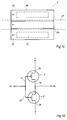
- Figure 1d shows the circuit diagram of the CMOS circuit.
- the drain contacts of the transistors are electrically connected together since they consist of one and the same metal layer 14.
- the source contact 13 of the transistor 2 is connected to a positive supply voltage
- the source contact 28 of the transistor 3 is connected to a negative supply voltage.
- the control electrodes 11 and 27 of the transistors are connected together and constitute the input of the circuit, to which an input signal Ui is supplied.
- the common drain contact 14 constitutes the output of the circuit, where the output signal Uu of the circuit is obtained.
- a space charge region forms at the N-transistor at the junction between the drain and channel region of the transistor.
- electron hole pairs are formed in the space charge region.
- the holes travel to the channel region and cause this to become charged, which acts in the same way as a positive control voltage.
- the non-linearity caused thereby is a disadvantage in the case of analog operation of the CMOS circuit. It is known that this disadvantage may be reduced if the channel region is connected to the source region (is "grounded").
- the source region is "grounded"
- it has proved to be difficult to bring about an effective improvement in this way primarily because the resistance between the source contact and the central parts of the channel region is high as a result of the weak doping of the region.
- known transistors of this kind possess less satisfactory high-frequency properties; further, they are impaired by noise caused by the state of the surface at the junction between the sapphire and the channel region.
- the MOS transistor described in Patent Abstracts of Japan, abstract of JP 51-147 186 (Fujitsu K.K.), December 17, 1976, is provided with a contact part of P-type between the source and the sapphire substrate and this contact part is shorted with the N-type source by the source electrode.
- the superficial part of the channel region must have low doping - a doping dose of the order of magnitude of at most 1011 cm ⁇ 2 - for the threshold voltage of the transistor to receive a useful value.
- Radioactive radiation for example gamma rays, produces a positive charge of the sapphire, whereby an N-channel is induced in the surface of the slightly doped channel region, which surface faces the sapphire.
- a transistor of the above kind consists of a main portion on the plane surface of the silicon layer and two "corner transistors" 31 and 32. Since the control electrode at the corners 31 and 32 influences the silicon layer from two directions, the effective threshold voltage will be lower (and thus the leakage currents higher) at the corners than on the plane surface of the transistor. It has also been found that the silicon oxide layer 26 becomes thicker at the edges below the corners 31 and 32. This causes the threshold voltage there to become more radiation-sensitive than for the main portion. Taken together, these effects at the corners and edges lead to a deterioration of the properties of the transistor as a whole. The requirements for accurate control of the manufacturing process will therefore be high to avoid that this deterioration becomes too great.
- the invention aims to provide a transistor of the above-mentioned kind, which exhibits a high constant gain, improved high frequency properties, low noise, lower leakage currents (and hence lower losses), and a low radiation sensitivity, which permits the use of narrower channel regions and hence lower operating voltages, and which places lower demands on the control of the manufacturing process in view of the properties of the transistors at the edges of the transistors.
- the invention suggests a transistor according to the introductory part of Claim 1, which is characterized by the features of the characterizing part of Claim 1.
- Figure 2a shows a section through a CMOS circuit with the transistor pair 2,3.
- the two transistors are formed in two silicon layers arranged on a sapphire base 1.
- an arbitrarily insulating material with suitable properties may be used, for example aluminium oxide or a silicon oxide layer arranged on a silicon base.
- the thickness of the silicon layer may be 0.3 to 0.6 ⁇ m.
- the source, drain and control contacts 13,28,14,11,27 and the insulating and protective layers 10,26,12 have the same design as in the case of the circuit shown in Figure 1a.
- the P-transistor 2 has the source region 4 and the drain region 6,7.
- the latter has a more highly doped part 6 arranged nearest the silicon surface, and a more weakly doped part 7 arranged nearest the sapphire base.
- the channel region has a more weakly doped part 9 and a more heavily doped part 8 located at a lower level.
- the latter doped part 8 extends laterally in under the source region 4 and is connected to a heavily doped part 5 arranged at the surfaces OF the silicon layer
- the source contact 13 also contacts the region 5.
- the drain region 20, 25 of the N-transistor 3 has a superficial highly doped part 20 and a part 25, located at a lower level, with a weaker doping.
- the channel region has a more weakly doped part 24 located nearest the surface, and a more heavily doped part 23 located nearer to the sapphire base, the latter part extending laterally in under the source region 22 and being connected, via a highly doped region 21, to the source contact 28.
- the different regions have been generated by ion implantation of dopants, for example phosphorous for the N-conducting regions and boron for the P-conducting regions.
- the doping dose is, for example, P-/N- 1011 cm ⁇ 2 P/N 1013 cm ⁇ 2 P+/N+ 1015 - 1016 cm ⁇ 2
- the doping dose of the more heavily doped parts 8 and 23 of the channel regions should exceed 2-3 x 1012 cm ⁇ 2 in order to obtain the favourable properties of a device according to the invention.
- Figure 2b shows a plan view of the N-transistor 3 with the source and drain contacts 28,14 shown in dashed lines.
- the transistor has the cross-section shown in Figure 2a along its entire length.
- the P-transistor 2 is constructed in the same way.
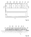
- Figure 3a shows a plan view of an N-transistor
- Figure 3b shows a section at A-A through this transistor.
- the P+ layer 21 as shown in Figure 2, extending along the length of the entire transistor, a plurality of separate layers 21a to 21c are arranged on top of the P layer 23, according to Figure 3, and distributed along the transistor.
- the source region 22 is divided into a plurality of separate regions 22a to 22d.
- the number of P+ layers may be both greater and smaller than in Figure 3 (three). Also, only one single P+ layer with a similar embodiment as the layer 21b in Figure 3 may be arranged.
- the P+ layers 21 need not, as in Figure 3, extend all the way to the channel region 24 but may terminate at a distance therefrom, the source region 22 becoming thereby one single cam-shaped, coherent region.
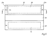
- Figure 4a shows a plan view of and Figure 4b, the latter exhibiting a section B-B through an N-transistor according to the invention. It differs from that shown in Figure 2 by the P+ layer 21 at both ends of the transistor having portions extending to the channel region 24. This eliminates the "corner transistor parts" 31 and 32 in Figure 1b. This gives, inter alia, the following considerable advantages,
- the "edge stop” according to Figure 4 can be used, as shown in Figure 4, together with a grounding of the channel region.
- it can be used in such a transistor in which the channel region is not grounded to the source contact.
- the width of the "edge stop”, i.e. the extension along the control electrode counting from the edge, should be at least as large as the thickness of the silicon layer.
- Figure 6 shows a further N-transistor. It corresponds to the N-transistor shown in Figure 2 with the exception that the lower, more heavily doped part 23 of the channel region does not extend to the drain region 20,25.
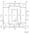
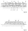
- Figure 7 shows a so-called closed transistor, i.e. a transistor in which the channel region is surrounded by the source or drain region (in the case shown in Figure 7 by the source region) of the transistor.
- Figure 7a shows a plan view of a closed N-transistor, Figure 7b a section taken along A-A in Figure 7a, and Figure 7c a section taken along B-B in Figure 7a.
- the reference numerals correspond to those used in Figure 2.
- the drain region 20,25 of the transistor is located in the centre thereof.
- the drain region is surrounded by the channel region 24 with its more heavily doped part 23, located at a lower level, which extends in under the source region 22, which in turn surrounds the channel region.
- P+ layers 21a to 21d are arranged between the layer 23 and the surface of the silicon layer.
- the drain contact 14 and the annular source contact 28 are shown in dashed lines in Figure 7a.
- the transistor according to Figure 7 exhibits the same advantages as the transistor shown in Figures 2 and 3, and since it is a closed transistor no problems with "corner transistors" arise. To render the grounding even more effective, the P+ region can be formed as in Figures 2 and 3.
Landscapes
- Thin Film Transistor (AREA)
- Metal-Oxide And Bipolar Metal-Oxide Semiconductor Integrated Circuits (AREA)
- Bipolar Transistors (AREA)
Claims (4)
- MOS-Transistor (3), der in einer Halbleiterschicht gebildet wird und auf einem isolierenden Substrat (1) angeordnet ist, mit- einem Kanalgebiet (24) eines ersten Leitungstyps (P), welches in der genannten Halbleiterschicht gebildet wird;- einem Source- (22) und einem Drain-Gebiete (20) eines zweiten Leitungstyps (N), welche durch ein Kanalgebiet (24) voneinander getrennt sind;- einem Source-Kontakt (28), der an das Source-Gebiet (22) angeschlossen ist;- einem Drain-Kontakt (14), der an das Drain-Gebiet (20) angeschlossen ist;- einer Steuerelektrode (27), die auf dem Kanalgebiet (24) angeordnet ist und durch eine Isolierschicht (26) von diesem getrennt ist, wobei das Kanalgebiet (24) und die Steuerelektrode (27) sich bis zu gegenüberliegenden Rändern der Halbleiterschicht erstrecken;- einem Bodengebiet (23) des ersten Leitungstyps (P), das unter dem Source-Gebiet (22) liegt, wobei das Bodengebiet (23) an die Kanalschicht (24) angrenzt und stärker dotiert ist als die Kanalschicht (24);dadurch gekennzeichnet,- daß ein Randbarrierengebiet (21) des ersten Leitungstyps (P) vorhanden ist, das an das Source-Gebiet (22), das Bodengebiet (23) und die Oberfläche der Halbleiterschicht angrenzt,- und daß das Randbarrierengebiet (21) und das Bodengebiet (23) das Source-Gebiet (22) vollständig von dem Substrat (1) und von den Rändern der Halbleiterschicht trennt.
- MOS-Transistor nach Anspruch 1, dadurch gekennzeichnet, daß das Randbarrierengebiet (21) stärker dotiert ist als das Bodengebiet (23).
- MOS-Transistor nach einem der Ansprüche 1 oder 2 dadurch gekennzeichnet, daß der Source-Kontakt (28) mit dem Randbarrierengebiet (21) verbunden ist.
- MOS-Transistor nach einem der vorhergehenden Ansprüche, daß das Bodengebiet (23) mit einem Dotierungsgrad von mindestens 2 x 10¹² cm⁻² dotiert ist.
Applications Claiming Priority (2)
| Application Number | Priority Date | Filing Date | Title |
|---|---|---|---|
| SE8703269A SE461490B (sv) | 1987-08-24 | 1987-08-24 | Mos-transistor utbildad paa ett isolerande underlag |
| SE8703269 | 1987-08-24 |
Publications (2)
| Publication Number | Publication Date |
|---|---|
| EP0304811A1 EP0304811A1 (de) | 1989-03-01 |
| EP0304811B1 true EP0304811B1 (de) | 1993-05-26 |
Family
ID=20369361
Family Applications (1)
| Application Number | Title | Priority Date | Filing Date |
|---|---|---|---|
| EP88113464A Expired - Lifetime EP0304811B1 (de) | 1987-08-24 | 1988-08-19 | MOS-Transistor |
Country Status (5)
| Country | Link |
|---|---|
| US (1) | US4969023A (de) |
| EP (1) | EP0304811B1 (de) |
| JP (1) | JPS6468970A (de) |
| DE (1) | DE3881304T2 (de) |
| SE (1) | SE461490B (de) |
Families Citing this family (33)
| Publication number | Priority date | Publication date | Assignee | Title |
|---|---|---|---|---|
| US5144390A (en) * | 1988-09-02 | 1992-09-01 | Texas Instruments Incorporated | Silicon-on insulator transistor with internal body node to source node connection |
| JP2507567B2 (ja) * | 1988-11-25 | 1996-06-12 | 三菱電機株式会社 | 絶縁体基板上の半導体層に形成されたmos型電界効果トランジスタ |
| US5160989A (en) * | 1989-06-13 | 1992-11-03 | Texas Instruments Incorporated | Extended body contact for semiconductor over insulator transistor |
| FR2648623B1 (fr) * | 1989-06-19 | 1994-07-08 | France Etat | Structure de transistor mos sur isolant avec prise de caisson reliee a la source et procede de fabrication |
| US5316960A (en) * | 1989-07-11 | 1994-05-31 | Ricoh Company, Ltd. | C-MOS thin film transistor device manufacturing method |
| US5060035A (en) * | 1989-07-13 | 1991-10-22 | Mitsubishi Denki Kabushiki Kaisha | Silicon-on-insulator metal oxide semiconductor device having conductive sidewall structure |
| US5264720A (en) * | 1989-09-22 | 1993-11-23 | Nippondenso Co., Ltd. | High withstanding voltage transistor |
| JP2994670B2 (ja) | 1989-12-02 | 1999-12-27 | 忠弘 大見 | 半導体装置及びその製造方法 |
| US5172208A (en) * | 1990-07-30 | 1992-12-15 | Texas Instruments Incorporated | Thyristor |
| US5240865A (en) * | 1990-07-30 | 1993-08-31 | Texas Instruments Incorporated | Method of forming a thyristor on an SOI substrate |
| TW214603B (en) * | 1992-05-13 | 1993-10-11 | Seiko Electron Co Ltd | Semiconductor device |
| KR940022907A (ko) * | 1993-03-31 | 1994-10-21 | 이헌조 | 비대칭 엘디디(ldd) 접합 박막트랜지스터 |
| US5773864A (en) * | 1995-04-28 | 1998-06-30 | National Semiconductor Corporation | CMOS interface circuit formed in silicon-on-insulator substrate |
| JPH09102609A (ja) * | 1995-08-03 | 1997-04-15 | Seiko Instr Inc | 半導体装置 |
| KR20000003758A (ko) * | 1998-06-29 | 2000-01-25 | 김영환 | 박막 트랜지스터 액정표시소자 |
| US6452233B1 (en) * | 1999-03-23 | 2002-09-17 | Citizen Watch Co., Ltd. | SOI device having a leakage stopping layer |
| JP2002261292A (ja) * | 2000-12-26 | 2002-09-13 | Toshiba Corp | 半導体装置及びその製造方法 |
| JP3845272B2 (ja) * | 2001-06-19 | 2006-11-15 | シャープ株式会社 | Sram及びその製造方法 |
| JP2003031811A (ja) | 2001-07-13 | 2003-01-31 | Mitsubishi Heavy Ind Ltd | トランジスタ及び半導体装置 |
| EP1498958B1 (de) * | 2003-07-18 | 2014-10-15 | Imec | Herstellungsverfahren für ein Halbleiterbauelement mit mehrfachem Gate |
| EP1519421A1 (de) | 2003-09-25 | 2005-03-30 | Interuniversitair Microelektronica Centrum Vzw | Halbleiterbauelement mit mehrfachem Gate und diesbezügliches Herstellungsverfahren |
| TWI463526B (zh) * | 2004-06-24 | 2014-12-01 | 萬國商業機器公司 | 改良具應力矽之cmos元件的方法及以該方法製備而成的元件 |
| US7655511B2 (en) | 2005-11-03 | 2010-02-02 | International Business Machines Corporation | Gate electrode stress control for finFET performance enhancement |
| US7635620B2 (en) | 2006-01-10 | 2009-12-22 | International Business Machines Corporation | Semiconductor device structure having enhanced performance FET device |
| US20070158743A1 (en) * | 2006-01-11 | 2007-07-12 | International Business Machines Corporation | Thin silicon single diffusion field effect transistor for enhanced drive performance with stress film liners |
| US7790540B2 (en) | 2006-08-25 | 2010-09-07 | International Business Machines Corporation | Structure and method to use low k stress liner to reduce parasitic capacitance |
| KR101312259B1 (ko) * | 2007-02-09 | 2013-09-25 | 삼성전자주식회사 | 박막 트랜지스터 및 그 제조방법 |
| US8115254B2 (en) | 2007-09-25 | 2012-02-14 | International Business Machines Corporation | Semiconductor-on-insulator structures including a trench containing an insulator stressor plug and method of fabricating same |
| US8492846B2 (en) | 2007-11-15 | 2013-07-23 | International Business Machines Corporation | Stress-generating shallow trench isolation structure having dual composition |
| US8598006B2 (en) | 2010-03-16 | 2013-12-03 | International Business Machines Corporation | Strain preserving ion implantation methods |
| JP2012256928A (ja) * | 2012-08-15 | 2012-12-27 | Mitsubishi Heavy Ind Ltd | トランジスタ及び半導体装置 |
| JP2015035617A (ja) * | 2014-10-15 | 2015-02-19 | 三菱重工業株式会社 | トランジスタ及び半導体装置 |
| JP6263162B2 (ja) * | 2015-12-21 | 2018-01-17 | 三菱重工業株式会社 | トランジスタ |
Family Cites Families (10)
| Publication number | Priority date | Publication date | Assignee | Title |
|---|---|---|---|---|
| US3958266A (en) * | 1974-04-19 | 1976-05-18 | Rca Corporation | Deep depletion insulated gate field effect transistors |
| JPS5534582B2 (de) * | 1974-06-24 | 1980-09-08 | ||
| JPS51147186A (en) * | 1975-06-12 | 1976-12-17 | Fujitsu Ltd | Semiconductor device |
| JPS5727069A (en) * | 1980-07-25 | 1982-02-13 | Toshiba Corp | Mos type simiconductor device |
| JPS57190362A (en) * | 1981-05-19 | 1982-11-22 | Nec Corp | Semiconductor device |
| JPS5898969A (ja) * | 1981-12-09 | 1983-06-13 | Nec Corp | 半導体装置 |
| JPS6115369A (ja) * | 1984-07-02 | 1986-01-23 | Nippon Telegr & Teleph Corp <Ntt> | 半導体装置及びその製造方法 |
| JPH0680830B2 (ja) * | 1985-04-08 | 1994-10-12 | 株式会社日立製作所 | 半導体装置 |
| JPH0682840B2 (ja) * | 1985-09-25 | 1994-10-19 | 日本電信電話株式会社 | Mos形半導体装置 |
| US4797721A (en) * | 1987-04-13 | 1989-01-10 | General Electric Company | Radiation hardened semiconductor device and method of making the same |
-
1987
- 1987-08-24 SE SE8703269A patent/SE461490B/sv not_active IP Right Cessation
-
1988
- 1988-08-19 DE DE88113464T patent/DE3881304T2/de not_active Expired - Fee Related
- 1988-08-19 EP EP88113464A patent/EP0304811B1/de not_active Expired - Lifetime
- 1988-08-23 US US07/235,075 patent/US4969023A/en not_active Expired - Fee Related
- 1988-08-23 JP JP63207493A patent/JPS6468970A/ja active Pending
Also Published As
| Publication number | Publication date |
|---|---|
| SE8703269D0 (sv) | 1987-08-24 |
| DE3881304T2 (de) | 1993-12-16 |
| EP0304811A1 (de) | 1989-03-01 |
| JPS6468970A (en) | 1989-03-15 |
| SE461490B (sv) | 1990-02-19 |
| DE3881304D1 (de) | 1993-07-01 |
| US4969023A (en) | 1990-11-06 |
| SE8703269L (sv) | 1989-02-25 |
Similar Documents
| Publication | Publication Date | Title |
|---|---|---|
| EP0304811B1 (de) | MOS-Transistor | |
| EP0110313B1 (de) | Integrierte Halbleiterschaltungsanordnung und Herstellungsverfahren | |
| US6060750A (en) | Semiconductor device having SOI-MOSFET | |
| US4734752A (en) | Electrostatic discharge protection device for CMOS integrated circuit outputs | |
| US5321287A (en) | Semiconductor device wherein n-channel MOSFET, p-channel MOSFET and nonvolatile memory cell are formed in one chip | |
| US4908682A (en) | Power MOSFET having a current sensing element of high accuracy | |
| EP0458570A1 (de) | Diode und Halbleiterbauelement mit einer Diode | |
| JPS6237545B2 (de) | ||
| US4631562A (en) | Zener diode structure | |
| US5838033A (en) | Integrated circuit with gate conductor defined resistor | |
| US5990520A (en) | Method for fabricating a high performance vertical bipolar NPN or PNP transistor having low base resistance in a standard CMOS process | |
| JP2800702B2 (ja) | 半導体装置 | |
| EP0031238B1 (de) | Halbleiterspeichervorrichtung | |
| JP2814079B2 (ja) | 半導体集積回路とその製造方法 | |
| EP0220500B1 (de) | Halbleitervorrichtung mit verringerter kapazitiver Belastung und deren Herstellungsverfahren | |
| EP0263287A2 (de) | Herstellung eines Kondensators in einer integrierten Schaltung | |
| US4864380A (en) | Edgeless CMOS device | |
| US4651178A (en) | Dual inverse zener diode with buried junctions | |
| EP0399454B1 (de) | Monolithische Halbleiteranordnung mit CCD-, bipolaren und MOS-Strukturen | |
| JP2864576B2 (ja) | 半導体装置 | |
| US4918498A (en) | Edgeless semiconductor device | |
| JPH0440865B2 (de) | ||
| KR900002886B1 (ko) | 반도체 기억장치 | |
| US5122855A (en) | Semiconductor device with latch-up prevention structure | |
| US6429490B2 (en) | Protection device and protection method for semiconductor device |
Legal Events
| Date | Code | Title | Description |
|---|---|---|---|
| PUAI | Public reference made under article 153(3) epc to a published international application that has entered the european phase |
Free format text: ORIGINAL CODE: 0009012 |
|
| AK | Designated contracting states |
Kind code of ref document: A1 Designated state(s): CH DE FR GB IT LI |
|
| 17P | Request for examination filed |
Effective date: 19890619 |
|
| 17Q | First examination report despatched |
Effective date: 19910828 |
|
| GRAA | (expected) grant |
Free format text: ORIGINAL CODE: 0009210 |
|
| AK | Designated contracting states |
Kind code of ref document: B1 Designated state(s): CH DE FR GB IT LI |
|
| REF | Corresponds to: |
Ref document number: 3881304 Country of ref document: DE Date of ref document: 19930701 |
|
| ET | Fr: translation filed | ||
| ITF | It: translation for a ep patent filed | ||
| PLBE | No opposition filed within time limit |
Free format text: ORIGINAL CODE: 0009261 |
|
| STAA | Information on the status of an ep patent application or granted ep patent |
Free format text: STATUS: NO OPPOSITION FILED WITHIN TIME LIMIT |
|
| 26N | No opposition filed | ||
| PGFP | Annual fee paid to national office [announced via postgrant information from national office to epo] |
Ref country code: GB Payment date: 19960812 Year of fee payment: 9 |
|
| PGFP | Annual fee paid to national office [announced via postgrant information from national office to epo] |
Ref country code: CH Payment date: 19960905 Year of fee payment: 9 |
|
| PG25 | Lapsed in a contracting state [announced via postgrant information from national office to epo] |
Ref country code: GB Free format text: LAPSE BECAUSE OF NON-PAYMENT OF DUE FEES Effective date: 19970819 |
|
| PG25 | Lapsed in a contracting state [announced via postgrant information from national office to epo] |
Ref country code: LI Free format text: LAPSE BECAUSE OF NON-PAYMENT OF DUE FEES Effective date: 19970831 Ref country code: CH Free format text: LAPSE BECAUSE OF NON-PAYMENT OF DUE FEES Effective date: 19970831 |
|
| GBPC | Gb: european patent ceased through non-payment of renewal fee |
Effective date: 19970819 |
|
| REG | Reference to a national code |
Ref country code: CH Ref legal event code: PL |
|
| PGFP | Annual fee paid to national office [announced via postgrant information from national office to epo] |
Ref country code: FR Payment date: 19980814 Year of fee payment: 11 |
|
| PGFP | Annual fee paid to national office [announced via postgrant information from national office to epo] |
Ref country code: DE Payment date: 19980831 Year of fee payment: 11 |
|
| PG25 | Lapsed in a contracting state [announced via postgrant information from national office to epo] |
Ref country code: FR Free format text: LAPSE BECAUSE OF NON-PAYMENT OF DUE FEES Effective date: 20000428 |
|
| PG25 | Lapsed in a contracting state [announced via postgrant information from national office to epo] |
Ref country code: DE Free format text: LAPSE BECAUSE OF NON-PAYMENT OF DUE FEES Effective date: 20000601 |
|
| REG | Reference to a national code |
Ref country code: FR Ref legal event code: ST |
|
| PG25 | Lapsed in a contracting state [announced via postgrant information from national office to epo] |
Ref country code: IT Free format text: LAPSE BECAUSE OF NON-PAYMENT OF DUE FEES;WARNING: LAPSES OF ITALIAN PATENTS WITH EFFECTIVE DATE BEFORE 2007 MAY HAVE OCCURRED AT ANY TIME BEFORE 2007. THE CORRECT EFFECTIVE DATE MAY BE DIFFERENT FROM THE ONE RECORDED. Effective date: 20050819 |