EP0304901A2 - Dispositif utilisé pour la modification et/ou la réparation de voies conductrices déposées sur un panneau comportant des éléments montés en surface - Google Patents
Dispositif utilisé pour la modification et/ou la réparation de voies conductrices déposées sur un panneau comportant des éléments montés en surface Download PDFInfo
- Publication number
- EP0304901A2 EP0304901A2 EP88113813A EP88113813A EP0304901A2 EP 0304901 A2 EP0304901 A2 EP 0304901A2 EP 88113813 A EP88113813 A EP 88113813A EP 88113813 A EP88113813 A EP 88113813A EP 0304901 A2 EP0304901 A2 EP 0304901A2
- Authority
- EP
- European Patent Office
- Prior art keywords
- circuit board
- components
- printed circuit
- conductor tracks
- arrangement
- Prior art date
- Legal status (The legal status is an assumption and is not a legal conclusion. Google has not performed a legal analysis and makes no representation as to the accuracy of the status listed.)
- Granted
Links
Images
Classifications
-
- H—ELECTRICITY
- H05—ELECTRIC TECHNIQUES NOT OTHERWISE PROVIDED FOR
- H05K—PRINTED CIRCUITS; CASINGS OR CONSTRUCTIONAL DETAILS OF ELECTRIC APPARATUS; MANUFACTURE OF ASSEMBLAGES OF ELECTRICAL COMPONENTS
- H05K1/00—Printed circuits
- H05K1/02—Details
- H05K1/11—Printed elements for providing electric connections to or between printed circuits
- H05K1/111—Pads for surface mounting, e.g. lay-out
- H05K1/112—Pads for surface mounting, e.g. lay-out directly combined with via connections
-
- H—ELECTRICITY
- H05—ELECTRIC TECHNIQUES NOT OTHERWISE PROVIDED FOR
- H05K—PRINTED CIRCUITS; CASINGS OR CONSTRUCTIONAL DETAILS OF ELECTRIC APPARATUS; MANUFACTURE OF ASSEMBLAGES OF ELECTRICAL COMPONENTS
- H05K1/00—Printed circuits
- H05K1/02—Details
- H05K1/0286—Programmable, customizable or modifiable circuits
- H05K1/0292—Programmable, customizable or modifiable circuits having a modifiable lay-out, i.e. adapted for engineering changes or repair
-
- H—ELECTRICITY
- H05—ELECTRIC TECHNIQUES NOT OTHERWISE PROVIDED FOR
- H05K—PRINTED CIRCUITS; CASINGS OR CONSTRUCTIONAL DETAILS OF ELECTRIC APPARATUS; MANUFACTURE OF ASSEMBLAGES OF ELECTRICAL COMPONENTS
- H05K1/00—Printed circuits
- H05K1/02—Details
- H05K1/0296—Conductive pattern lay-out details not covered by sub groups H05K1/02 - H05K1/0295
- H05K1/0298—Multilayer circuits
-
- H—ELECTRICITY
- H05—ELECTRIC TECHNIQUES NOT OTHERWISE PROVIDED FOR
- H05K—PRINTED CIRCUITS; CASINGS OR CONSTRUCTIONAL DETAILS OF ELECTRIC APPARATUS; MANUFACTURE OF ASSEMBLAGES OF ELECTRICAL COMPONENTS
- H05K2201/00—Indexing scheme relating to printed circuits covered by H05K1/00
- H05K2201/09—Shape and layout
- H05K2201/09209—Shape and layout details of conductors
- H05K2201/09218—Conductive traces
- H05K2201/09227—Layout details of a plurality of traces, e.g. escape layout for Ball Grid Array [BGA] mounting
-
- H—ELECTRICITY
- H05—ELECTRIC TECHNIQUES NOT OTHERWISE PROVIDED FOR
- H05K—PRINTED CIRCUITS; CASINGS OR CONSTRUCTIONAL DETAILS OF ELECTRIC APPARATUS; MANUFACTURE OF ASSEMBLAGES OF ELECTRICAL COMPONENTS
- H05K2201/00—Indexing scheme relating to printed circuits covered by H05K1/00
- H05K2201/09—Shape and layout
- H05K2201/09209—Shape and layout details of conductors
- H05K2201/09654—Shape and layout details of conductors covering at least two types of conductors provided for in H05K2201/09218 - H05K2201/095
- H05K2201/09772—Conductors directly under a component but not electrically connected to the component
-
- H—ELECTRICITY
- H05—ELECTRIC TECHNIQUES NOT OTHERWISE PROVIDED FOR
- H05K—PRINTED CIRCUITS; CASINGS OR CONSTRUCTIONAL DETAILS OF ELECTRIC APPARATUS; MANUFACTURE OF ASSEMBLAGES OF ELECTRICAL COMPONENTS
- H05K2201/00—Indexing scheme relating to printed circuits covered by H05K1/00
- H05K2201/10—Details of components or other objects attached to or integrated in a printed circuit board
- H05K2201/10227—Other objects, e.g. metallic pieces
- H05K2201/10287—Metal wires as connectors or conductors
-
- H—ELECTRICITY
- H05—ELECTRIC TECHNIQUES NOT OTHERWISE PROVIDED FOR
- H05K—PRINTED CIRCUITS; CASINGS OR CONSTRUCTIONAL DETAILS OF ELECTRIC APPARATUS; MANUFACTURE OF ASSEMBLAGES OF ELECTRICAL COMPONENTS
- H05K2201/00—Indexing scheme relating to printed circuits covered by H05K1/00
- H05K2201/10—Details of components or other objects attached to or integrated in a printed circuit board
- H05K2201/10613—Details of electrical connections of non-printed components, e.g. special leads
- H05K2201/10621—Components characterised by their electrical contacts
- H05K2201/10689—Leaded Integrated Circuit [IC] package, e.g. dual-in-line [DIL]
-
- H—ELECTRICITY
- H05—ELECTRIC TECHNIQUES NOT OTHERWISE PROVIDED FOR
- H05K—PRINTED CIRCUITS; CASINGS OR CONSTRUCTIONAL DETAILS OF ELECTRIC APPARATUS; MANUFACTURE OF ASSEMBLAGES OF ELECTRICAL COMPONENTS
- H05K3/00—Apparatus or processes for manufacturing printed circuits
- H05K3/40—Forming printed elements for providing electric connections to or between printed circuits
- H05K3/42—Plated through-holes or plated via connections
- H05K3/429—Plated through-holes specially for multilayer circuits, e.g. having connections to inner circuit layers
Definitions
- the etched conductor track of the circuit board which is no longer required, is usually mechanically separated and the new connection is established with the aid of a wire.
- connection spots of the SMD components on the circuit board have instead been made larger and made separable.
- this method has the disadvantage of the larger space requirement for the SMD component and the loss of plated-through holes on the printed circuit board.
- the invention was therefore based on the object of providing an arrangement with the aid of which changes and / or repairs to printed circuit boards can also be carried out when these are equipped with so-called SMD or similar components.
- the change and / or repair wiring can only be carried out on one side of the circuit board and therefore no change of the two sides of the circuit board Wires are required, and that the pads for the change and / or Repair wiring is virtually in the shadow of the connection spots for the SMD modules and therefore no additional space is required or no through-connection options are blocked.
- the arrangement according to the invention provides good prerequisites for a mechanical change method, such as a so-called written circuit.
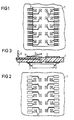
- the SMD module 2 is so large in relation to the soldering spots on the circuit board that it is not possible to solder change and / or repair wires to the soldering spots.
- a second conductor pattern 4 is therefore provided, as shown in FIG. 2. This is preferably congruent with the conductor pattern 3 located directly under the building blocks 2 and is flush with it. 3, on the side of the circuit board 1 facing away from the components 2, and its conductor tracks 4 are connected to the conductor tracks 3 on the other side of the circuit board via plated-through holes 6.
- FIG. 3 also indicates how, in the event of a change in the circuit, a conductor track 7 located inside the circuit board 1 can be separated with the aid of a drill 8 and replaced by a change wire 5.
Landscapes
- Engineering & Computer Science (AREA)
- Microelectronics & Electronic Packaging (AREA)
- Manufacturing Of Printed Wiring (AREA)
- Multi-Conductor Connections (AREA)
- Production Of Multi-Layered Print Wiring Board (AREA)
- Structures For Mounting Electric Components On Printed Circuit Boards (AREA)
- Printing Elements For Providing Electric Connections Between Printed Circuits (AREA)
- Structure Of Printed Boards (AREA)
- Combinations Of Printed Boards (AREA)
Priority Applications (1)
| Application Number | Priority Date | Filing Date | Title |
|---|---|---|---|
| AT88113813T ATE79506T1 (de) | 1987-08-28 | 1988-08-24 | Anordnung zum aendern und/oder reparieren von flachbaugruppen bei bestueckung mit smdbausteinen. |
Applications Claiming Priority (2)
| Application Number | Priority Date | Filing Date | Title |
|---|---|---|---|
| DE8711697U DE8711697U1 (de) | 1987-08-28 | 1987-08-28 | Vorrichtung zum Ändern und/oder Reparieren von Flachbaugruppen bei Bestückung mit SMD-Bausteinen |
| DE8711697U | 1987-08-28 |
Publications (3)
| Publication Number | Publication Date |
|---|---|
| EP0304901A2 true EP0304901A2 (fr) | 1989-03-01 |
| EP0304901A3 EP0304901A3 (en) | 1989-09-20 |
| EP0304901B1 EP0304901B1 (fr) | 1992-08-12 |
Family
ID=6811532
Family Applications (1)
| Application Number | Title | Priority Date | Filing Date |
|---|---|---|---|
| EP88113813A Expired - Lifetime EP0304901B1 (fr) | 1987-08-28 | 1988-08-24 | Dispositif utilisé pour la modification et/ou la réparation de voies conductrices déposées sur un panneau comportant des éléments montés en surface |
Country Status (3)
| Country | Link |
|---|---|
| EP (1) | EP0304901B1 (fr) |
| AT (1) | ATE79506T1 (fr) |
| DE (2) | DE8711697U1 (fr) |
Family Cites Families (2)
| Publication number | Priority date | Publication date | Assignee | Title |
|---|---|---|---|---|
| DE3025875A1 (de) * | 1980-07-08 | 1982-02-04 | Siemens AG, 1000 Berlin und 8000 München | Vorrichtung zur reparatur von leiterbahnunterbrechungen |
| GB2124835B (en) * | 1982-08-03 | 1986-04-30 | Burroughs Corp | Current printed circuit boards |
-
1987
- 1987-08-28 DE DE8711697U patent/DE8711697U1/de not_active Expired
-
1988
- 1988-08-24 DE DE8888113813T patent/DE3873661D1/de not_active Expired - Lifetime
- 1988-08-24 AT AT88113813T patent/ATE79506T1/de not_active IP Right Cessation
- 1988-08-24 EP EP88113813A patent/EP0304901B1/fr not_active Expired - Lifetime
Also Published As
| Publication number | Publication date |
|---|---|
| DE3873661D1 (de) | 1992-09-17 |
| EP0304901A3 (en) | 1989-09-20 |
| DE8711697U1 (de) | 1987-11-12 |
| ATE79506T1 (de) | 1992-08-15 |
| EP0304901B1 (fr) | 1992-08-12 |
Similar Documents
| Publication | Publication Date | Title |
|---|---|---|
| DE10325550B4 (de) | Elektrisches Kontaktierungsverfahren | |
| DE2233578A1 (de) | Mehrschichtige gedruckte schaltungsplatte | |
| DE4134617A1 (de) | Verbindungsvorrichtung mit in gleicher ebene liegenden kontakthoeckern und das verfahren zur herstellung einer derartigen vorrichtung | |
| DE2539925A1 (de) | Verfahren zur herstellung einer mehrschichtigen gedruckten schaltungsplatte | |
| DE10111718A1 (de) | Elektronisches Schaltungsbauteil | |
| DE4020498C2 (de) | Verfahren zum Herstellen von Multiwire-Leiterplatten mit isolierten Metalleitern und/oder optischen Leitern | |
| AT398676B (de) | Leiterplattenanordnung | |
| DE3810486C2 (fr) | ||
| EP0304901B1 (fr) | Dispositif utilisé pour la modification et/ou la réparation de voies conductrices déposées sur un panneau comportant des éléments montés en surface | |
| DE1930642A1 (de) | Leiterplatte zum Aufnehmen und Verbinden elektrischer Bauelemente | |
| EP0304902B1 (fr) | Dispositif utilisé pour la modification et/ou la réparation des voies conductrices portées par un panneau comportant des composants montés en surface | |
| DE102008013226A1 (de) | Hochfeste Lötverbindung für SMD Bauteile | |
| DE102012112546A1 (de) | Verfahren zur Herstellung von mischbestückten Leiterplatten | |
| DE19712879A1 (de) | Verfahren zum Herstellen einer Schaltung und zugehöriges Nutzen | |
| EP0073489A2 (fr) | Module électrique | |
| DE3743163A1 (de) | Gedruckte leiterplatte fuer einen elektrischen schaltkreis, insbesondere in einer bueromaschine | |
| DE19802580A1 (de) | Elektrischer Schaltungsträger | |
| DE2021546B1 (de) | Leiterplatte fuer gedruckte Schaltungen | |
| DE2314566A1 (de) | Schaltkarte und verfahren zur herstellung der schaltkarte | |
| DE4204459A1 (de) | Filmtraegermontierter integrierter baustein | |
| DE102016226257A1 (de) | Mehrlagige leiterkarte und verfahren zum herstellen einer solchen mehrlagigen leiterkarte | |
| DE19601388A1 (de) | Leiterplatten-Trägervorrichtung | |
| DE4302196C2 (de) | Verfahren zum Ändern einer Teilfunktion einer elektrischen Baugruppe | |
| DE3240425A1 (de) | Miniatur-drahtbruecke zum herstellen von verbindungen auf baugruppen | |
| DE7016524U (de) | Leiterplatte fuer gedruckte schaltungen. |
Legal Events
| Date | Code | Title | Description |
|---|---|---|---|
| PUAI | Public reference made under article 153(3) epc to a published international application that has entered the european phase |
Free format text: ORIGINAL CODE: 0009012 |
|
| AK | Designated contracting states |
Kind code of ref document: A2 Designated state(s): AT BE CH DE FR GB IT LI NL |
|
| PUAL | Search report despatched |
Free format text: ORIGINAL CODE: 0009013 |
|
| AK | Designated contracting states |
Kind code of ref document: A3 Designated state(s): AT BE CH DE FR GB IT LI NL |
|
| 17P | Request for examination filed |
Effective date: 19891026 |
|
| RAP1 | Party data changed (applicant data changed or rights of an application transferred) |
Owner name: SIEMENS NIXDORF INFORMATIONSSYSTEME AG |
|
| 17Q | First examination report despatched |
Effective date: 19911118 |
|
| GRAA | (expected) grant |
Free format text: ORIGINAL CODE: 0009210 |
|
| AK | Designated contracting states |
Kind code of ref document: B1 Designated state(s): AT BE CH DE FR GB IT LI NL |
|
| REF | Corresponds to: |
Ref document number: 79506 Country of ref document: AT Date of ref document: 19920815 Kind code of ref document: T |
|
| REF | Corresponds to: |
Ref document number: 3873661 Country of ref document: DE Date of ref document: 19920917 |
|
| ET | Fr: translation filed | ||
| ITF | It: translation for a ep patent filed | ||
| GBT | Gb: translation of ep patent filed (gb section 77(6)(a)/1977) | ||
| PLBE | No opposition filed within time limit |
Free format text: ORIGINAL CODE: 0009261 |
|
| STAA | Information on the status of an ep patent application or granted ep patent |
Free format text: STATUS: NO OPPOSITION FILED WITHIN TIME LIMIT |
|
| PGFP | Annual fee paid to national office [announced via postgrant information from national office to epo] |
Ref country code: GB Payment date: 19930714 Year of fee payment: 6 |
|
| PGFP | Annual fee paid to national office [announced via postgrant information from national office to epo] |
Ref country code: AT Payment date: 19930716 Year of fee payment: 6 |
|
| 26N | No opposition filed | ||
| PGFP | Annual fee paid to national office [announced via postgrant information from national office to epo] |
Ref country code: BE Payment date: 19930818 Year of fee payment: 6 |
|
| PGFP | Annual fee paid to national office [announced via postgrant information from national office to epo] |
Ref country code: FR Payment date: 19930819 Year of fee payment: 6 |
|
| PGFP | Annual fee paid to national office [announced via postgrant information from national office to epo] |
Ref country code: NL Payment date: 19930831 Year of fee payment: 6 |
|
| PGFP | Annual fee paid to national office [announced via postgrant information from national office to epo] |
Ref country code: CH Payment date: 19931116 Year of fee payment: 6 |
|
| PG25 | Lapsed in a contracting state [announced via postgrant information from national office to epo] |
Ref country code: GB Effective date: 19940824 Ref country code: AT Effective date: 19940824 |
|
| PG25 | Lapsed in a contracting state [announced via postgrant information from national office to epo] |
Ref country code: LI Effective date: 19940831 Ref country code: CH Effective date: 19940831 Ref country code: BE Effective date: 19940831 |
|
| PGFP | Annual fee paid to national office [announced via postgrant information from national office to epo] |
Ref country code: DE Payment date: 19941018 Year of fee payment: 7 |
|
| BERE | Be: lapsed |
Owner name: SIEMENS NIXDORF INFORMATIONSSYSTEME A.G. Effective date: 19940831 |
|
| PG25 | Lapsed in a contracting state [announced via postgrant information from national office to epo] |
Ref country code: NL Effective date: 19950301 |
|
| NLV4 | Nl: lapsed or anulled due to non-payment of the annual fee | ||
| GBPC | Gb: european patent ceased through non-payment of renewal fee |
Effective date: 19940824 |
|
| PG25 | Lapsed in a contracting state [announced via postgrant information from national office to epo] |
Ref country code: FR Effective date: 19950428 |
|
| REG | Reference to a national code |
Ref country code: CH Ref legal event code: PL |
|
| REG | Reference to a national code |
Ref country code: FR Ref legal event code: ST |
|
| PG25 | Lapsed in a contracting state [announced via postgrant information from national office to epo] |
Ref country code: DE Effective date: 19960501 |
|
| PG25 | Lapsed in a contracting state [announced via postgrant information from national office to epo] |
Ref country code: IT Free format text: LAPSE BECAUSE OF NON-PAYMENT OF DUE FEES;WARNING: LAPSES OF ITALIAN PATENTS WITH EFFECTIVE DATE BEFORE 2007 MAY HAVE OCCURRED AT ANY TIME BEFORE 2007. THE CORRECT EFFECTIVE DATE MAY BE DIFFERENT FROM THE ONE RECORDED. Effective date: 20050824 |