EP0305709A2 - Multiplicateur matrice-matrice - Google Patents
Multiplicateur matrice-matrice Download PDFInfo
- Publication number
- EP0305709A2 EP0305709A2 EP88111445A EP88111445A EP0305709A2 EP 0305709 A2 EP0305709 A2 EP 0305709A2 EP 88111445 A EP88111445 A EP 88111445A EP 88111445 A EP88111445 A EP 88111445A EP 0305709 A2 EP0305709 A2 EP 0305709A2
- Authority
- EP
- European Patent Office
- Prior art keywords
- multiplicand
- elements
- matrix
- lines
- line
- Prior art date
- Legal status (The legal status is an assumption and is not a legal conclusion. Google has not performed a legal analysis and makes no representation as to the accuracy of the status listed.)
- Granted
Links
Images
Classifications
-
- G—PHYSICS
- G06—COMPUTING OR CALCULATING; COUNTING
- G06F—ELECTRIC DIGITAL DATA PROCESSING
- G06F17/00—Digital computing or data processing equipment or methods, specially adapted for specific functions
- G06F17/10—Complex mathematical operations
- G06F17/16—Matrix or vector computation, e.g. matrix-matrix or matrix-vector multiplication, matrix factorization
Definitions
- the invention relates to a circuit for multiplying the elements of a multiplicand matrix by the elements of a multiplier matrix according to the preambles of claims 1 and 2.
- the invention has for its object to provide a circuit of the type mentioned above, which can be integrated on a doped semiconductor body to save space. This is achieved according to the invention by designing the circuit according to the characterizing parts of patent claims 1 or 2.
- the advantage that can be achieved with the invention is, in particular, that a plurality of bit-specific circuits or double-bit-specific circuits, which are used to multiply the digital signals representing the elements of the multiplicand matrix by the digital signals representing the elements of the multiplier matrix, can be implemented in a very space-saving manner, so that the entire circuit can be implemented on a relatively small semiconductor area.
- the multiplication of the elements Xij of a multiplicand matrix with the elements Yij of a multiplier matrix can be represented as follows for two elements per row and column:
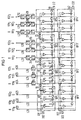
- the circuit shown in FIG. 1 for carrying out this matrix-matrix multiplication has a first multiplicand line with a plurality of sections L11 to L14, the input E11 of which is supplied with digital signals which represent the elements X11 and X12 of the first line of the X-matrix. These signals are fed at a sampling rate of 1 / T.
- L11 is connected to a first bit-specific circuit BP1. This consists of three multiplier lines L21 to L23, the inputs E21 to E23 of which are supplied in a manner to be described in more detail the least significant bits Yij0 of the signals which represent the elements of the Y matrix.
- BP1 contains a chain circuit of adders 4 and 5 and delay elements 6, 7 and 8, which are alternately connected to the chain with adders 4 and 5.
- the output of partial product stage 1 is connected via delay element 6 to one input of adder 4, the other input of which is connected to the output of partial product stage 2.
- the output of 4 is connected via the delay element 7 to the first input of the adder 5, the other input of which is connected to the output of the partial product stage 3.
- the output of the delay element 8 connected downstream of the adder 5 represents the output of the chain circuit of BP1.
- the second section L12 of the first multiplicand line is connected in an analogous manner to a correspondingly constructed, bit-specific circuit BP2, the three multiplier lines L24 to L26, three partial product stages 9 to 11 and a chain circuit consisting of the adders 12 to 14 and with these alternating delay elements 15 to 17, contains.
- the section L12 is connected to the section L11 via a delay chain 18 which simulates the delay which is given by the links 6, 7 and 8 of BP1.
- the signals supplied via E11 and tapped at the output of 18 are thus synchronized with the intermediate results occurring at the output of the delay element 8.
- the lines L24 to L26 are fed via their inputs E24 to E26, the bits Yij1 of the second lowest order.
- the derailleur 12, 15, 13, 16, 14 and 17 of BP2 is directly connected to the output of the derailleur of BP1.
- Delay elements 19 to 21, which emulate the delay of the delay chain 18, are inserted into the lines L24 to L26 of BP2.
- Section L13 of the multiplicand line is connected to L12 via a delay chain 22, section L14 via another delay chain 23 to L13.
- the bit-specific circuit BP3 connected to L13 and the circuit BP4 connected to L14 are constructed in accordance with BP2.
- the multiplier lines L27 to L29 are occupied with the signal bits Yij2 of the valence 22 and the lines L210 to L212 with the signal bits Yij3 of the highest valence 23.
- delay elements 24, 25 and 26 are inserted, which emulate the delays of the delay chains 18 and 22, while in L210 to L212 delay elements 27 to 29 are activated, which emulate the delays of the chains 18, 22 and 23.
- the chain connection of BP3 is connected to the output of the chain connection of BP2, the chain connection of BP4 to the output of the chain connection of BP3.
- Digital signals corresponding to elements C11 and C12 of the first line of the product matrix can then be tapped at the output A1 of the chain circuit of BP4.
- a further subcircuit which has an input E12 and an output A2. Between these two connections, it is designed in the same way as the previously described first subcircuit between the Connections E11 and A1.
- the line connected to E12 is to be referred to as a second multiplicand line, the four sections of which are separated from one another by delay chains and are each connected to bit-specific circuits BP1 'to BP4'.
- the multiplier lines L21 to L212 are extended so far without the interposition of further delay elements that they also pass through the circuits BP1 'to BP4'.
- the delay elements 19 to 21, 24 to 26 and 27 to 29 are thus assigned to the circuits BP2 and BP2 ', BP3 and BP3' and the circuits BP4 and BP4 'together.
- the signals X21 and X22, which represent the elements of the second line of the X matrix, are fed to E12, signals C21 and C22, which represent the elements of the second line of the product matrix, can be tapped at A2.
- signals X11 and X21 are present at inputs E11 and E12 during a sampling period T n .
- signals X12 and X22 are applied to E11 and E12, while lines L21 to L23 with "0", Y210 and Y220, lines L24 to L26 with "0", Y211 and Y221 , the lines L27 to L29 with 1 "0", Y212 and Y222 and the lines L210 to L212 with "0", Y213 and Y223 are assigned.
- Signals C12 and C22 then appear at A1 and A2 within a later sampling period and signals C11 and C21 within the subsequent sampling period.
- the inputs E11 and E12 each consist of n connections.
- the multiplicand lines connected to these then each have n lines which are used for the bit-parallel transmission of the signals Xij.
- Each of the partial product stages, for example 1 is designed as a line-shaped arrangement of n gates, for example AND gates, while the adders, for example 4, each consist of a line-shaped arrangement of full adders, each for bit-parallel addition of two n-digit input signals are required.
- the use of carry save adder stages or carry ripple adder stages with additional pipelining in the transmission direction of the carry signals has proven to be particularly advantageous.
- the number of multiplier lines, for example L21 to L23, assigned to a bit-specific circuit, for example BP1, corresponds generally to the number m of row elements of the Y matrix, increased by the number of these rows of the matrix reduced by 1.
- T n the signals which represent the line elements of the first line of the Y matrix are fed to the first m multiplier lines of a bit-specific circuit, starting with the line furthest to the left in FIG. 1, but not with these signals more busy lines are assigned a 0.
- the signals which represent the elements of the second line of the Y matrix are applied offset by one line to the right, again the lines which are not occupied in this case are each connected with a "0".
- the number of sections of the multiplicand lines and the number of bit-specific circuits generally corresponds to the word width of the Yij signals. If the word width p of these signals is greater than 4, the number of sections shown in FIG. 1 increases to L1p and the number of bit-specific circuits to BPp. Furthermore, the number of multiplicand lines corresponds to the number of lines in the X matrix, the signals which correspond to the elements of the matrix line assigned to this line being fed to the input of each multiplicand line.
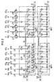
- the exemplary embodiment shown in FIG. 2 differs from FIG. 1 in that the bit-specific circuits BP1 and BP2 are combined to form a double-bit-specific circuit DBP1.
- BP3 and BP4 are also combined to form a double-bit-specific circuit DBP2.
- the lines L21, L24, L22, L25, L23 and L26 are arranged side by side in this order.
- the partial product stages 1, 9, 2, 10, 3 and 11 are also provided in this order in addition to the associated multiplier lines.
- the first inputs of partial product stages 1, 2 and 3 and so far have been connected directly to section L112 of the first multiplicand line, but the first inputs of partial product stages 9, 10 and 11 are via a delay stage 30.
- the second inputs of 1, 9, 2, 10, 3 and 11 are each connected to the associated multiplier lines L21 to L26, delay lines 31, 32 and 33 being inserted in lines L24, L25 and L26.
- the output of partial product stage 1 is connected via a delay stage 34 to one input of adder 35, the other input of which is connected to the output of partial product stage 9.
- the output of 35 is connected via a delay stage 36 to one input of an adder 37, the other input of which is connected to the output of 2 in Connection is established.
- the output of 37 is connected via a delay stage 38 to an adder 39, the other input of which is connected to the output of 10.
- the output of 39 is in turn connected via a delay stage 40 to the one input of an adder 41, the other input of which is connected to the output of 3.
- the output of 41 is connected via a delay stage 42 to the first input of an adder 43, the other input of which is connected to the output of 11.
- the output of a delay stage 44 connected downstream of the output of 43 represents the output of a chain circuit of DBP1, which consists of adders 35, 37, 39, 41 and 43 and delay stages 34, 36, 38, 40, 42 and 44.
- DBP2 double-bit-specific circuit
- the output of 1 could also be connected to the input of an adder, the other input of which would be connected to a "0" and the output of which would then be at the input of 34, without the function of DBP1 being changed.
- Delay stages 49 to 54 are inserted into the multiplier lines L27 to L212, which simulate the delay of the chain 45. The signals corresponding to the first line of the product matrix can be picked up again at output A1 of the derailleur circuit of DBP2.
- a further subcircuit is located between E12 and A2 in FIG. 2, which completely corresponds to the subcircuit arranged between the connections E11 and A1.
- the signals which correspond to the elements of the second line of the X matrix are again fed to E12, the signals corresponding to the elements of the second line of the product matrix being tapped at A2.
- the double bit specific circuits the lower sub-circuit are designated with DBP1 'and DBP2'.
- the multiplier lines L2 to L212 are assigned the same signals in FIG. 2 as in FIG. 1.
- the delay stages shown in Fig. 2, e.g. 30, 31 to 33, 34, 36, 48 etc. are preferably in register half steps, e.g. as D flip-flops, and each cause a delay that corresponds to half a sampling period of the signals supplied at E11 and E12.
- the delay stages 49 to 54 each cause a delay of three sampling periods.
Landscapes
- Engineering & Computer Science (AREA)
- Physics & Mathematics (AREA)
- General Physics & Mathematics (AREA)
- Mathematical Physics (AREA)
- Pure & Applied Mathematics (AREA)
- Mathematical Analysis (AREA)
- Mathematical Optimization (AREA)
- Computational Mathematics (AREA)
- Data Mining & Analysis (AREA)
- Theoretical Computer Science (AREA)
- Computing Systems (AREA)
- Algebra (AREA)
- Databases & Information Systems (AREA)
- Software Systems (AREA)
- General Engineering & Computer Science (AREA)
- Complex Calculations (AREA)
Applications Claiming Priority (2)
| Application Number | Priority Date | Filing Date | Title |
|---|---|---|---|
| DE3729175 | 1987-09-01 | ||
| DE3729175 | 1987-09-01 |
Publications (3)
| Publication Number | Publication Date |
|---|---|
| EP0305709A2 true EP0305709A2 (fr) | 1989-03-08 |
| EP0305709A3 EP0305709A3 (en) | 1990-11-14 |
| EP0305709B1 EP0305709B1 (fr) | 1993-12-29 |
Family
ID=6334970
Family Applications (1)
| Application Number | Title | Priority Date | Filing Date |
|---|---|---|---|
| EP88111445A Expired - Lifetime EP0305709B1 (fr) | 1987-09-01 | 1988-07-15 | Multiplicateur matrice-matrice |
Country Status (4)
| Country | Link |
|---|---|
| US (1) | US4841469A (fr) |
| EP (1) | EP0305709B1 (fr) |
| JP (1) | JPS6472262A (fr) |
| DE (1) | DE3886625D1 (fr) |
Cited By (1)
| Publication number | Priority date | Publication date | Assignee | Title |
|---|---|---|---|---|
| NL9200899A (nl) * | 1992-02-13 | 1993-09-01 | Ind Tech Res Inst | Snelle volgens de pijplijnmethode werkende matrixvermenigvuldiger. |
Families Citing this family (7)
| Publication number | Priority date | Publication date | Assignee | Title |
|---|---|---|---|---|
| US5021987A (en) * | 1989-08-31 | 1991-06-04 | General Electric Company | Chain-serial matrix multipliers |
| US5170370A (en) * | 1989-11-17 | 1992-12-08 | Cray Research, Inc. | Vector bit-matrix multiply functional unit |
| JPH03167664A (ja) * | 1989-11-28 | 1991-07-19 | Nec Corp | マトリクス演算回路 |
| US5099447A (en) * | 1990-01-22 | 1992-03-24 | Alliant Computer Systems Corporation | Blocked matrix multiplication for computers with hierarchical memory |
| US5226002A (en) * | 1991-06-28 | 1993-07-06 | Industrial Technology Research Institute | Matrix multiplier circuit |
| US5483475A (en) * | 1993-09-15 | 1996-01-09 | Industrial Technology Research Institute | Fast pipelined 2-D discrete cosine transform architecture |
| US5481487A (en) * | 1994-01-28 | 1996-01-02 | Industrial Technology Research Institute | Transpose memory for DCT/IDCT circuit |
Family Cites Families (6)
| Publication number | Priority date | Publication date | Assignee | Title |
|---|---|---|---|---|
| GB2141847B (en) * | 1983-05-06 | 1986-10-15 | Seiko Instr & Electronics | Matrix multiplication apparatus for graphic display |
| US4697247A (en) * | 1983-06-10 | 1987-09-29 | Hughes Aircraft Company | Method of performing matrix by matrix multiplication |
| GB2144245B (en) * | 1983-07-28 | 1987-07-29 | Secr Defence | A digital data processor for matrix/matrix multiplication |
| GB8320362D0 (en) * | 1983-07-28 | 1983-09-01 | Secr Defence | Digital data processor |
| US4787057A (en) * | 1986-06-04 | 1988-11-22 | General Electric Company | Finite element analysis method using multiprocessor for matrix manipulations with special handling of diagonal elements |
| US4763365A (en) * | 1987-04-15 | 1988-08-16 | Tolo, Inc. | Spa system having high temperature safety device |
-
1988
- 1988-07-15 DE DE88111445T patent/DE3886625D1/de not_active Expired - Fee Related
- 1988-07-15 EP EP88111445A patent/EP0305709B1/fr not_active Expired - Lifetime
- 1988-07-22 US US07/222,937 patent/US4841469A/en not_active Expired - Fee Related
- 1988-08-30 JP JP63218202A patent/JPS6472262A/ja active Pending
Cited By (1)
| Publication number | Priority date | Publication date | Assignee | Title |
|---|---|---|---|---|
| NL9200899A (nl) * | 1992-02-13 | 1993-09-01 | Ind Tech Res Inst | Snelle volgens de pijplijnmethode werkende matrixvermenigvuldiger. |
Also Published As
| Publication number | Publication date |
|---|---|
| US4841469A (en) | 1989-06-20 |
| EP0305709B1 (fr) | 1993-12-29 |
| DE3886625D1 (de) | 1994-02-10 |
| EP0305709A3 (en) | 1990-11-14 |
| JPS6472262A (en) | 1989-03-17 |
Similar Documents
| Publication | Publication Date | Title |
|---|---|---|
| DE1549477B1 (de) | Einrichtung zur schnellen akkumulation einer anzahl mehr stelliger binaerer operanden | |
| EP0305709B1 (fr) | Multiplicateur matrice-matrice | |
| DE1809219A1 (de) | Binaeres Vielfach-Addierwerk zur gleichzeitigen Addition mehrerer binaerer Zahlen | |
| DE3889150T2 (de) | Filter n-ten Ranges. | |
| EP0305708B1 (fr) | Filtre numérique à décimation | |
| DE4215094A1 (de) | Bildverarbeitungsverfahren und -vorrichtung | |
| DE69026414T2 (de) | Binäres Addiergerät | |
| DE2732008B2 (de) | Einrichtung zur Reduzierung von Fibonacci-p-Codes auf die Minimalform | |
| DE69230924T2 (de) | Multiplizierer-Schaltungen mit seriellem Eingang | |
| DE69320681T2 (de) | Digitales Filter | |
| DE3878666T2 (de) | Integrierte schaltung fuer digitale rechenvorgaenge zur faltung oder aehnlichen rechenverfahren. | |
| DE3524797A1 (de) | Anordnung zur bitparallelen addition von binaerzahlen | |
| DE3889746T2 (de) | Zähler. | |
| EP0424410B1 (fr) | Multiplicateur | |
| EP0489952B1 (fr) | Dipositif de circuit à traitement de données digital sériel par bit | |
| DE19525781A1 (de) | Pseudo-Zufallsmuster-Generatorschaltung | |
| EP0433315A1 (fr) | Circuits d'addition ou de soustraction d'operandes codes selon un code bcd ou dual | |
| EP0752130B1 (fr) | Multiplicateur a duree d'execution reduite | |
| EP0333884A1 (fr) | Circuit multiplieur parallèle-série ainsi que ses étages de multiplication et d'addition | |
| DE4014767A1 (de) | Verfahren zum gewinnen eines elektrischen signals durch korrelation | |
| DE69713349T2 (de) | Benutzerprogrammierbarer analogprozessor | |
| EP0407903B1 (fr) | Système de transmission d'information MIC avec un dispositif de synchronisation du récepteur répondant aux mots insérés dans l'information transmise | |
| EP0239599B1 (fr) | Circuit transformateur | |
| DE10139099C2 (de) | Carry-Ripple Addierer | |
| DE2657404B2 (de) | Steuerwerk |
Legal Events
| Date | Code | Title | Description |
|---|---|---|---|
| PUAI | Public reference made under article 153(3) epc to a published international application that has entered the european phase |
Free format text: ORIGINAL CODE: 0009012 |
|
| AK | Designated contracting states |
Kind code of ref document: A2 Designated state(s): DE FR GB IT NL |
|
| PUAL | Search report despatched |
Free format text: ORIGINAL CODE: 0009013 |
|
| AK | Designated contracting states |
Kind code of ref document: A3 Designated state(s): DE FR GB IT NL |
|
| 17P | Request for examination filed |
Effective date: 19901221 |
|
| 17Q | First examination report despatched |
Effective date: 19930525 |
|
| GRAA | (expected) grant |
Free format text: ORIGINAL CODE: 0009210 |
|
| AK | Designated contracting states |
Kind code of ref document: B1 Designated state(s): DE FR GB IT NL |
|
| REF | Corresponds to: |
Ref document number: 3886625 Country of ref document: DE Date of ref document: 19940210 |
|
| ITF | It: translation for a ep patent filed | ||
| GBT | Gb: translation of ep patent filed (gb section 77(6)(a)/1977) |
Effective date: 19940307 |
|
| ET | Fr: translation filed | ||
| PLBE | No opposition filed within time limit |
Free format text: ORIGINAL CODE: 0009261 |
|
| STAA | Information on the status of an ep patent application or granted ep patent |
Free format text: STATUS: NO OPPOSITION FILED WITHIN TIME LIMIT |
|
| 26N | No opposition filed | ||
| PGFP | Annual fee paid to national office [announced via postgrant information from national office to epo] |
Ref country code: DE Payment date: 19960917 Year of fee payment: 9 |
|
| PGFP | Annual fee paid to national office [announced via postgrant information from national office to epo] |
Ref country code: GB Payment date: 19970620 Year of fee payment: 10 |
|
| PGFP | Annual fee paid to national office [announced via postgrant information from national office to epo] |
Ref country code: NL Payment date: 19970714 Year of fee payment: 10 |
|
| PGFP | Annual fee paid to national office [announced via postgrant information from national office to epo] |
Ref country code: FR Payment date: 19970718 Year of fee payment: 10 |
|
| PG25 | Lapsed in a contracting state [announced via postgrant information from national office to epo] |
Ref country code: DE Free format text: LAPSE BECAUSE OF NON-PAYMENT OF DUE FEES Effective date: 19980401 |
|
| PG25 | Lapsed in a contracting state [announced via postgrant information from national office to epo] |
Ref country code: GB Free format text: LAPSE BECAUSE OF NON-PAYMENT OF DUE FEES Effective date: 19980715 |
|
| PG25 | Lapsed in a contracting state [announced via postgrant information from national office to epo] |
Ref country code: NL Free format text: LAPSE BECAUSE OF NON-PAYMENT OF DUE FEES Effective date: 19990201 |
|
| GBPC | Gb: european patent ceased through non-payment of renewal fee |
Effective date: 19980715 |
|
| PG25 | Lapsed in a contracting state [announced via postgrant information from national office to epo] |
Ref country code: FR Free format text: LAPSE BECAUSE OF NON-PAYMENT OF DUE FEES Effective date: 19990331 |
|
| NLV4 | Nl: lapsed or anulled due to non-payment of the annual fee |
Effective date: 19990201 |
|
| REG | Reference to a national code |
Ref country code: FR Ref legal event code: ST |
|
| PG25 | Lapsed in a contracting state [announced via postgrant information from national office to epo] |
Ref country code: IT Free format text: LAPSE BECAUSE OF NON-PAYMENT OF DUE FEES Effective date: 20050715 |