EP0306225A2 - Verfahren zur Herstellung eines Halbleiterlasers - Google Patents
Verfahren zur Herstellung eines Halbleiterlasers Download PDFInfo
- Publication number
- EP0306225A2 EP0306225A2 EP88307899A EP88307899A EP0306225A2 EP 0306225 A2 EP0306225 A2 EP 0306225A2 EP 88307899 A EP88307899 A EP 88307899A EP 88307899 A EP88307899 A EP 88307899A EP 0306225 A2 EP0306225 A2 EP 0306225A2
- Authority
- EP
- European Patent Office
- Prior art keywords
- layer
- producing
- semiconductor laser
- neighborhood
- end surface
- Prior art date
- Legal status (The legal status is an assumption and is not a legal conclusion. Google has not performed a legal analysis and makes no representation as to the accuracy of the status listed.)
- Granted
Links
Images
Classifications
-
- H—ELECTRICITY
- H10—SEMICONDUCTOR DEVICES; ELECTRIC SOLID-STATE DEVICES NOT OTHERWISE PROVIDED FOR
- H10H—INORGANIC LIGHT-EMITTING SEMICONDUCTOR DEVICES HAVING POTENTIAL BARRIERS
- H10H20/00—Individual inorganic light-emitting semiconductor devices having potential barriers, e.g. light-emitting diodes [LED]
- H10H20/01—Manufacture or treatment
- H10H20/011—Manufacture or treatment of bodies, e.g. forming semiconductor layers
- H10H20/013—Manufacture or treatment of bodies, e.g. forming semiconductor layers having light-emitting regions comprising only Group III-V materials
-
- H—ELECTRICITY
- H01—ELECTRIC ELEMENTS
- H01S—DEVICES USING THE PROCESS OF LIGHT AMPLIFICATION BY STIMULATED EMISSION OF RADIATION [LASER] TO AMPLIFY OR GENERATE LIGHT; DEVICES USING STIMULATED EMISSION OF ELECTROMAGNETIC RADIATION IN WAVE RANGES OTHER THAN OPTICAL
- H01S5/00—Semiconductor lasers
- H01S5/10—Construction or shape of the optical resonator, e.g. extended or external cavity, coupled cavities, bent-guide, varying width, thickness or composition of the active region
- H01S5/1053—Comprising an active region having a varying composition or cross-section in a specific direction
- H01S5/106—Comprising an active region having a varying composition or cross-section in a specific direction varying thickness along the optical axis
-
- H—ELECTRICITY
- H01—ELECTRIC ELEMENTS
- H01S—DEVICES USING THE PROCESS OF LIGHT AMPLIFICATION BY STIMULATED EMISSION OF RADIATION [LASER] TO AMPLIFY OR GENERATE LIGHT; DEVICES USING STIMULATED EMISSION OF ELECTROMAGNETIC RADIATION IN WAVE RANGES OTHER THAN OPTICAL
- H01S5/00—Semiconductor lasers
- H01S5/10—Construction or shape of the optical resonator, e.g. extended or external cavity, coupled cavities, bent-guide, varying width, thickness or composition of the active region
- H01S5/16—Window-type lasers, i.e. with a region of non-absorbing material between the active region and the reflecting surface
Definitions
- the present invention relates to a semiconductor laser and a method of producing same, and more particularly to that method capable of obtaining a semiconductor laser having a narrow emission beam and a high light output property by conducting film production at good controllability and uniform quality on a large area wafer.
- semiconductor lasers are often used as a light source in light communication, an optical disk, and a laser printer.
- properties such as narrow emission beam, high output operation, low threshold current, and lengthy lifetime are strongly desired.
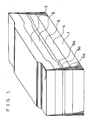
- Figure 4 shows an example of a substrate of such a semiconductor laser in its processed state
- figure 5 shows a perspective view of a structure of a semiconductor laser which is obtained by conducting epitaxial growths of respective semiconductor layers successively on the substrate.
- the center portion of the laser is cut and position shifted for easening the understanding.
- the reference numerals 4 and 4a designate lower cladding layers comprising n type Al x Ga 1-x As which are produced at the central portion of the chip and on the ridges 2, respectively.
- the reference numerals 5 and 5a designate active layers comprising Al y Ga 1-y As which are produced at the central portion of the chip and on the ridges 2, respectively.
- the reference numerals 6 and 6a designate upper cladding layers comprising p type Al x Ga 1-x As which are produced at the central portion of the chip and on the ridges 2, respectively.
- the reference numeral 7 designates a p type GaAs contact layer.
- LPE method a phenomenon peculiar to the liquid phase epitaxy
- the thickness of the active layer is constant in the light emission direction, and when the thickness of the active layer is made thin uniformly in order to realize the narrow emission beam and high output operation, the gain is reduced thereby to increase the threshold current, and overheating occurs due to such as increase in the light power density and that in the light absorption at the neighborhood of the resonator end surface, thereby shortening the lifetime of the laser element.
- the thickness of the active layer 5 at the inside and central portion of the chip which largely affects influences upon the lasing threshold current is made to be somewhat thick and only that at the neighborhood of the resonator end surface is made thin, whereby spreading of light into the upper and lower cladding layers 6a and 4a is increased and the light power density thereat is lowered.
- This and the accompanying reduction in the threshold current enable desired properties of lengthy lifetime, narrow emission beam, and high output operation.
- the layer thickness of the active layer at the neighborhood of the resonator end surface is made thinner than that at the inside and central portion of the chip by utilizing that the growth rate of the semiconductor layer in the LPE method is slower at the ridge portion than at the plain portion.
- the LPE method there is a limitation in the widening of the wafer area and this method is not desirable in view of the enhancement in the reproducibility, production yield, and quality.
- An object of the present invention is to provide a method of producing a semiconductor laser having properties of narrow emission beam, high output operation, low threshold current, and lengthy lifetime which is capable of conducting film production of semiconductor layers at good controllability, uniform quality, and high yield.
- Another object of the present invention is to provide a semiconductor laser having the above-described properties which is produced by the above-described method.
- At least a support layer and a mask layer are produced on a semiconductor substrate, and thereafter, these layers are etched and the support layer is side-etched thereby to produce an overhung portion of mask layer at above the semiconductor substrate at the neighborhood of the resonator end surface, and in this state a lower cladding layer, an active layer, and an upper cladding layer are successively grown on the substrate by an MOCVD method. Accordingly, the circulating of material gas into below the overhung portion mask layer becomes bad, and the amount of supplied gas thereto is reduced with relative to that to the other portion, and the growth rate of the film becomes slower.
- a doublehetero junction structure in which the thicknesses of the respective layers at the neighborhood of the light emission end surface are thinner than those at the inside and central portion of the chip is thus obtained.
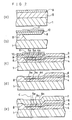
- Figure 1 shows a semiconductor laser as an embodiment of the present invention and figure 2 shows the production process thereof in the order of the processing steps.
- the same reference numerals designate the same or corresponding elements as those shown in figure 1.
- the reference numerals 8, 9, 10, and 11 designate layers constituting masks for producing the respective layers 4a to 6a. That is, the numeral 8 designates a support layer comprising n type Al x Ga 1-x As, the numeral 9 designates an n type GaAs mask layer, the numeral 10 designates a silicon dioxide film(SiO2 film), and the numeral 11 designates an overhung portion comprising the mask layer 9 and the SiO2 film 10, produced at the neighborhood of the light emission end surface.
- an overhung portion comprising at least a support layer and a mask layer is produced at an upper portion of the semiconductor substrate at the neighborhood of the resonator end surface, and in this state respective semiconductor layers are successively grown on the substrate by an MOCVD method, the circulating of material gas into below the overhung portion becomes bad, and the amount of supplied gas thereto is reduced with relative to that to the other portion, and the growth rate of the film becomes slower.
- a doublehetero junction structure in which the thicknesses of the respective layers at the neighborhood of the resonator end surface are thinner than those at the inside and central portion of the chip is obtained.
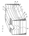
- FIG. 3 Another embodiment of the present invention of such a structure is shown in figure 3.
- the reference numeral 12 designates an n type GaAs current blocking layer
- the reference numeral 13 designates a stripe groove
- the reference numeral 14 designates a p type Al x Ga 1-x As embedded layer.
- the production processes of this embodiment are the same up to those of figures 2(a) to (d), and thereafter, an n type GaAs current blocking layer 12 is epitaxially grown, a stripe groove 13 is produced by etching the layer 12, and a p type Al x Ga 1-x As embedded layer 14 is epitaxially grown.
- the productions of the layers 12 and 14 are conducted by an MOCVD method.
- the processes thereafter are the same as those shown in figure 2(e).
- the active layer 5 is provided close to the current blocking layer 12 so as to constitute a light waveguide mechanism which enables a transverse mode control. Also the thickness of the active layer is made less at the neighborhood of the resonator end surface than at the inside and central portion of the chip, resulting in the same effects as those of the first embodiment.
- epitaxial growths of a lower cladding layer, an active layer, and an upper cladding layer which constitute a doublehetero junction are successively grown on the substrate by an MOCVD method in a state where an overhung portion of a mask layer is produced at above the semiconductor substrate at the neighborhood of the light emission end surface. Accordingly, the thicknesses of the respective layers at the neighborhood of the resonator end surface are made less than those at the inside and central portion of the chip, and a semiconductor laser having a narrow emission beam, a high output operation, a low threshold current, and a lengthy lifetime is obtained at a high production yield and uniform quality with good reproducibility.
Landscapes
- Physics & Mathematics (AREA)
- Condensed Matter Physics & Semiconductors (AREA)
- General Physics & Mathematics (AREA)
- Electromagnetism (AREA)
- Optics & Photonics (AREA)
- Semiconductor Lasers (AREA)
- Weting (AREA)
Applications Claiming Priority (2)
| Application Number | Priority Date | Filing Date | Title |
|---|---|---|---|
| JP62215586A JPS6457786A (en) | 1987-08-28 | 1987-08-28 | Manufacture of semiconductor laser device |
| JP215586/87 | 1987-08-28 |
Publications (3)
| Publication Number | Publication Date |
|---|---|
| EP0306225A2 true EP0306225A2 (de) | 1989-03-08 |
| EP0306225A3 EP0306225A3 (en) | 1989-06-14 |
| EP0306225B1 EP0306225B1 (de) | 1991-12-27 |
Family
ID=16674885
Family Applications (1)
| Application Number | Title | Priority Date | Filing Date |
|---|---|---|---|
| EP88307899A Expired - Lifetime EP0306225B1 (de) | 1987-08-28 | 1988-08-25 | Verfahren zur Herstellung eines Halbleiterlasers |
Country Status (3)
| Country | Link |
|---|---|
| EP (1) | EP0306225B1 (de) |
| JP (1) | JPS6457786A (de) |
| DE (1) | DE3867180D1 (de) |
Families Citing this family (1)
| Publication number | Priority date | Publication date | Assignee | Title |
|---|---|---|---|---|
| KR100404323B1 (ko) * | 2001-01-30 | 2003-11-03 | 한국전자통신연구원 | 성장 부위별 에피텍시 성장성이 다르게 반도체 에피텍시층을 성장시키는 방법 |
Family Cites Families (3)
| Publication number | Priority date | Publication date | Assignee | Title |
|---|---|---|---|---|
| US4447904A (en) * | 1981-02-04 | 1984-05-08 | Xerox Corporation | Semiconductor devices with nonplanar characteristics produced in chemical vapor deposition |
| JPS60192379A (ja) * | 1984-03-12 | 1985-09-30 | Mitsubishi Electric Corp | 半導体レ−ザ装置 |
| DE3678761D1 (de) * | 1985-07-15 | 1991-05-23 | Philips Nv | Verfahren zur herstellung einer halbleiteranordnung unter verwendung des aetzens einer ga-as-schicht mittels einer alkalischen loesung von wasserstoffperoxide. |
-
1987
- 1987-08-28 JP JP62215586A patent/JPS6457786A/ja active Pending
-
1988
- 1988-08-25 DE DE8888307899T patent/DE3867180D1/de not_active Expired - Lifetime
- 1988-08-25 EP EP88307899A patent/EP0306225B1/de not_active Expired - Lifetime
Also Published As
| Publication number | Publication date |
|---|---|
| EP0306225A3 (en) | 1989-06-14 |
| JPS6457786A (en) | 1989-03-06 |
| DE3867180D1 (de) | 1992-02-06 |
| EP0306225B1 (de) | 1991-12-27 |
Similar Documents
| Publication | Publication Date | Title |
|---|---|---|
| CA1225465A (en) | Fabrication of grooved semiconductor devices | |
| US5386428A (en) | Stacked active region laser array for multicolor emissions | |
| US5684823A (en) | Method of fabricating a diffraction grating and a distributed feedback semiconductor laser incorporating the diffraction grating | |
| US4667332A (en) | Semiconductor laser element suitable for production by a MO-CVD method | |
| CA1151775A (en) | Batch processing of semiconductor devices | |
| US5541950A (en) | Semiconductor laser including groove having variable dimensions | |
| US5737351A (en) | Semiconductor laser including ridge structure extending between window regions | |
| EP0157555B1 (de) | Halbleiterlaser und Verfahren zu dessen Fabrikation | |
| US5838028A (en) | Semiconductor device having a ridge or groove | |
| US5786234A (en) | Method of fabricating semiconductor laser | |
| US5524017A (en) | Quantum well semiconductor laser | |
| EP0306225B1 (de) | Verfahren zur Herstellung eines Halbleiterlasers | |
| JPH05327112A (ja) | 半導体レーザの製造方法 | |
| JP2629678B2 (ja) | 半導体レーザ装置およびその製造方法 | |
| JP2525788B2 (ja) | 半導体レ−ザ装置の製造方法 | |
| US5360763A (en) | Method for fabricating an optical semiconductor device | |
| JP2947164B2 (ja) | 半導体レーザ素子 | |
| JP3038424B2 (ja) | 埋め込み構造半導体レーザとその製造方法 | |
| JPH0634426B2 (ja) | 半導体レ−ザ装置の製造方法 | |
| JP2525776B2 (ja) | 半導体装置の製造方法 | |
| JPS6351558B2 (de) | ||
| JPH0831652B2 (ja) | 半導体レ−ザ | |
| US4725450A (en) | Method for fabricating a semiconductor laser device | |
| JP2547459B2 (ja) | 半導体レーザ素子及びその製造方法 | |
| JP3026389B2 (ja) | 半導体装置とその製造方法 |
Legal Events
| Date | Code | Title | Description |
|---|---|---|---|
| PUAI | Public reference made under article 153(3) epc to a published international application that has entered the european phase |
Free format text: ORIGINAL CODE: 0009012 |
|
| AK | Designated contracting states |
Kind code of ref document: A2 Designated state(s): DE FR GB |
|
| PUAL | Search report despatched |
Free format text: ORIGINAL CODE: 0009013 |
|
| AK | Designated contracting states |
Kind code of ref document: A3 Designated state(s): DE FR GB |
|
| 17P | Request for examination filed |
Effective date: 19890809 |
|
| 17Q | First examination report despatched |
Effective date: 19910121 |
|
| GRAA | (expected) grant |
Free format text: ORIGINAL CODE: 0009210 |
|
| AK | Designated contracting states |
Kind code of ref document: B1 Designated state(s): DE FR GB |
|
| REF | Corresponds to: |
Ref document number: 3867180 Country of ref document: DE Date of ref document: 19920206 |
|
| ET | Fr: translation filed | ||
| PLBE | No opposition filed within time limit |
Free format text: ORIGINAL CODE: 0009261 |
|
| STAA | Information on the status of an ep patent application or granted ep patent |
Free format text: STATUS: NO OPPOSITION FILED WITHIN TIME LIMIT |
|
| 26N | No opposition filed | ||
| REG | Reference to a national code |
Ref country code: GB Ref legal event code: 746 Effective date: 19950809 |
|
| REG | Reference to a national code |
Ref country code: FR Ref legal event code: D6 |
|
| REG | Reference to a national code |
Ref country code: GB Ref legal event code: IF02 |
|
| PGFP | Annual fee paid to national office [announced via postgrant information from national office to epo] |
Ref country code: FR Payment date: 20040810 Year of fee payment: 17 |
|
| PGFP | Annual fee paid to national office [announced via postgrant information from national office to epo] |
Ref country code: GB Payment date: 20040825 Year of fee payment: 17 |
|
| PGFP | Annual fee paid to national office [announced via postgrant information from national office to epo] |
Ref country code: DE Payment date: 20040902 Year of fee payment: 17 |
|
| PG25 | Lapsed in a contracting state [announced via postgrant information from national office to epo] |
Ref country code: GB Free format text: LAPSE BECAUSE OF NON-PAYMENT OF DUE FEES Effective date: 20050825 |
|
| PG25 | Lapsed in a contracting state [announced via postgrant information from national office to epo] |
Ref country code: DE Free format text: LAPSE BECAUSE OF NON-PAYMENT OF DUE FEES Effective date: 20060301 |
|
| GBPC | Gb: european patent ceased through non-payment of renewal fee |
Effective date: 20050825 |
|
| PG25 | Lapsed in a contracting state [announced via postgrant information from national office to epo] |
Ref country code: FR Free format text: LAPSE BECAUSE OF NON-PAYMENT OF DUE FEES Effective date: 20060428 |
|
| REG | Reference to a national code |
Ref country code: FR Ref legal event code: ST Effective date: 20060428 |