EP0306227A2 - Faseroptischer Fühler - Google Patents
Faseroptischer Fühler Download PDFInfo
- Publication number
- EP0306227A2 EP0306227A2 EP88307909A EP88307909A EP0306227A2 EP 0306227 A2 EP0306227 A2 EP 0306227A2 EP 88307909 A EP88307909 A EP 88307909A EP 88307909 A EP88307909 A EP 88307909A EP 0306227 A2 EP0306227 A2 EP 0306227A2
- Authority
- EP
- European Patent Office
- Prior art keywords
- optical
- reflector
- optical energy
- energy
- modulator
- Prior art date
- Legal status (The legal status is an assumption and is not a legal conclusion. Google has not performed a legal analysis and makes no representation as to the accuracy of the status listed.)
- Granted
Links
Images


Classifications
-
- G—PHYSICS
- G01—MEASURING; TESTING
- G01H—MEASUREMENT OF MECHANICAL VIBRATIONS OR ULTRASONIC, SONIC OR INFRASONIC WAVES
- G01H9/00—Measuring mechanical vibrations or ultrasonic, sonic or infrasonic waves by using radiation-sensitive means, e.g. optical means
- G01H9/004—Measuring mechanical vibrations or ultrasonic, sonic or infrasonic waves by using radiation-sensitive means, e.g. optical means using fibre optic sensors
Definitions
- This invention relates to fiber optic sensors.
- the invention particularly, but not exclusively, relates to fiber optic sensors utilized for detecting the signature of a marine seismic source.
- Fiber optic sensing system include elements whose characteristics change with time, thereby introducing error into the system unless means are included for compensating for such changes. These changes include variations in the intensity of the optical source and variations in the light transmitting capacity of the optical paths.
- U.S. Patent 4,162,397 shows an optical fiber acoustical sensor for detecting sound waves in a fluid medium.
- An optical fiber coil through which a light beam is transmitted is placed in a fluid medium.
- a sound wave propagating through the fluid medium and incident on the optical fiber coil changes the index of refraction of the optical fiber at the area of incidence.
- the change in the index of refraction causes a phase shift in the transmitted light which is detectable to denote the presence of the sound wave.
- This system does not include any means of correcting for changes in the sensing system with time.
- a reference channel is constructed in the time domain.
- a pulse modulated light source and fiber-optic loop are utilized.
- the light pulse is coupled by a 2 x 2 coupler into a fiber optic loop which includes the temperature probe.
- a portion of the pulsed energy exits the loop when it returns to the 2 x 2 coupler and a portion travels around the loop again, and when it returns to the coupler, a second portion exits the loop.
- the temperature is determined. Because the measurements are made of two pulse amplitudes having the same origin, and traversing the same path, the system substantially compensates for time-varying parameters.
- a disadvantage is that the entire fiber optic recirculating loop, including the sensor, acts a sensing element.
- the invention is an optical fiber sensor system.
- An optical source emits a light pulse which travels in an optical path to a light modulator.
- a first reflector is included upstream of the modulator and the optical path terminates in a second reflector behind the light modulator.
- the light pulse travels back from the terminating reflector to the first reflector and from that point the pulses reflected from the first reflector and the terminating reflector travel along the same path to a detection means, e.g. a photodetector and demodulator, where the magnitude of the parameter modulating the light modulator is determined from the relative magnitudes of the two reflected pulses.
- Optical energy source 2 which may be a laser diode, transmits an optical energy pulse through optical path 4, coupler 6 and optical path 16. In the particular embodiment described herein, this pulse may be 90 nanoseconds in duration.
- a portion of the optical energy is reflected by partial reflector 20.
- the remainder of the optical energy is coupler by coupler 15 into optical paths 25 and 27.
- the optical energy coupled into optical path 25 travels through light modulator 22 to reflector 24 at which point the energy is reflected.
- the optical energy coupled by coupler 15 into optical path 27 travels through light modulator 29 and is then reflected by reflector 28.
- Modulator 22 may be included in a housing 18 and modulator 29 may be included in a housing 21.
- Optical energy reflected by reflectors 20, 24 and 28 travels back along optical paths 16 and 8 until it reaches detector 10.
- the lengths of the optical paths between partial reflector 20 and reflector 24, and between partial reflector 20 and reflector 28, are selected so that the returning light pulses from the three reflectors are separated in time.
- a 10 nanosecond pulse separation is selected.
- Light travels about 20 meters in 100 nanoseconds. Therefore, in order to achieve a 10 nanosecond separation between the pulses reflected from partial reflector 20 and reflector 24, which will have pulse widths of 90 nanoseconds, the one-way optical path length between reflectors 20 and 24 is selected to be about 10 meters.
- the one-way optical path length between reflector 20 and reflector 28 is selected to be about 20 meters, to achieve a separation of 10 nanoseconds between the pulses reflected from reflectors 24 and 28.
- two light modulators are utilized.
- One of ordinary skill in the art would understand that only one light modulator might be utilized, and that the invention is extendible to more than two light modulators.
- the three returning pulses are detected by photodetector 10 which generates electrical signals having an amplitude corresponding to the magnitude of the reflected pulses. These electrical pulses are sampled in demodulator 12 to determine the magnitude of the modulating parameter sensed by the light modulators.
- the form of the light modulators 22 and 28 is not critical; the light modulators may be microbend sensors, moving grating sensors, or other types of sensors. We are concerned rather with compensating for variations in slowly varying changes within the system other than the dynamic parameter which is intended to be measured. These slowly varying, or steady state, changes include temperature changes, bending of the fiber, and electro-optical changes in the optical source and the optical paths. This compensation is achieved by comparing the signal magnitude reflected from partial reflector 20 to the signal magnitudes reflected from reflectors 24 and 28. Because the pulses will have traveled through the same path, except for the distances between partial reflector 20 and reflectors 24 and 28, the. system compensates for steady state changes in the system up to the point of partial reflector 20.
- the parameter to be measured might be the pressure wave generated by a marine seismic source.
- the optical energy source 2, photodetector 10, demodulator 12 and coupler 6 will normally be located on board the vessel; and partial reflector 20 and coupler 15 will be located close to light modulators 22 and 29, so that optical path 16 will be much longer than optical paths 25 and 27.
- Demodulator 12 is a timing and sampling unit. It generates the timing signal which causes laser diode 2 to emit a light pulse and controls sampling circuits for sampling the amplitude of the optical pulses reflected from reflectors 20, 24 and 28.
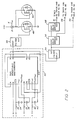
- FIG. 2 and 3 shows details of the electronic circuitry included in the demodulator. Shown in Figure 2 is a dual monostable multivibrator circuit 30.
- the circuit may comprise the SN74HC123 Retriggerable Monostable Multivibrator device from Texas Instruments.
- the two monostable multivibrators generate the control pulses for sending the light pulse to the light modulators and for detecting the return pulses.
- Resistor 36, capacitor 38, resistor 40 and capacitor 42 are selected by methods known to those of ordinary skill in the art for selecting the pulse widths of the output pulses from the two monostable multivibrators.
- Resistor 32 and capacitor 34 are utilized to delay the initiation of the first output pulse following power turn on and may preferably have a time constant of about one second. When capacitor 34 charges up, the 1Q and 1Q terminals are enabled to generate a first output pulse.
- Pulser 46 may comprise the TTLPGM-40 device made by Manby Engineered Components Company. In a preferred embodiment, this pulser is selected to have an output pulse width of about 90 nanoseconds.
- the output from pulser 46 controls the gates of MOSFETS (metal-oxide silicon field effect transistors) 48 and 50. During the 90 nanosecond output pulse, the two MOSFETS conduct current which flows through laser diode 2. The light from this laser diode then travels down optical path 4 to the light modulators.
- MOSFETS metal-oxide silicon field effect transistors
- Pulser 54 may also comprise the TTLPGM-40 device made by Manby Engineered Components Company.
- the output from pulser 54 is applied to the input of delay module 56.
- the output from delay module 56 is applied to the input of delay module 58.
- Delay modules 56 and 58 may comprise the TTLDL250 device made by Technitrol, Inc.
- the output signals from pulser 54, delay module 56 and delay module 58 are applied, via electrical conductors 59, 66 and 61, respectively, to the T/HLD terminals of track and hold circuits 62, 80 and 92, respectively, shown in Figure 3.
- the pulse width of the output pulse from pulser 54 is selected to be 40 nanoseconds.
- the output pulses from delay module 56 and delay module 58 may be substantially identical to the output from pulser 54 except that they are delayed in time by selected amounts.
- Pulser 54, delay module 56, and delay module 58 are configured so that the 40-nanosecond output pulses are at a low, or ZERO, state. The amount of delay is selected as a function of the physical dimensions of the system.
- the timing of the output pulses from pulser 54 and delay modules 56 and 58 are selected so that the 40 nanosecond low, or ZERO, level pulses are applied to the T/HLD terminals of track and hold circuits 68, 80 and 92, respectively, during the time period when the reflected optical energy pulses from reflectors 20, 24 and 28 are at the ANA IN terminals of the track and hold circuits.
- Figure 3 shows the detection portion of the system demodulator circuit.
- the light pulses return from reflectors 20, 24 and 28 via optical paths 16 and 8 and are detected by photodetector 10.
- the electrical output signal from the photodetector 10 is AC coupled through capacitor 112 to the analog input terminals (ANA IN) of track and hold circuits 62, 80 and 92.
- Track and hold circuits 62, 80 and 92 may comprise the HTC-0500 device made by Analog Devices.
- the track and hold circuit will track the input signal level applied to its ANA IN terminal.
- the signal level then at the ANA IN terminal will be "held” at the OUT terminal until the next transition to a ZERO level at the T/HLD input terminal.
- the monostable multivibrators When the power is initially turned on to the system and capacitor 34, which is connected to the ICLR terminal of the dual monostable multivibrator circuit 30, charges to a positive voltage, the monostable multivibrators are enabled to begin operation. Initially, a high, or ONE level, output pulse is generated at the 1Q output and simultaneously a ZERO-level pulse on the 1Q terminal. When the output from terminal 1Q goes low, an output pulse is generated on the 2Q and 2Q terminals, positive going on the 2Q terminal and negative going on the 2Q terminal. When the output from 2Q goes low, the output from the 1Q terminal goes up, and so on.
- Selection of the duration of the pulses will depend on the frequency at which it is desired to sample the modulating parameters to which modulators 22 and 27 are subjected, and on the transmission time of the optical pulse from the light source 2 to reflectors 20, 24 and 28 and back to photodetector 110.
- Pulser 46 initiates a pulse, enabling MOSFETS 48 and 40 to conduct current, upon detection of the trailing edge of the negative output pulse from the 1Q terminal of monostable circuits 30.
- the periods of the output pulses from the two monostables are selected so that there is sufficient time for the optical pulse to travel to the most distant of the reflectors (reflector 28 in the embodiment described herein) and to return before the next optical pulse is emitted.
- the output from track and hold circuit 62 passes through low-pass filter 65, unity gain amplifier 68 and amplifier 69.
- resistor 64 and capacitor 66 are selected so that filter 64 has a cut-off frequency at about 500 Hz.
- resistors 70, 71 and 73 are selected by methods known to those of ordinary skill in the art so that amplifier 69 has a gain of about six.
- the output signals from track and hold circuits 80 and 92 are passed through a low pass filter 83, amplifier 86 and amplifier 87; and low pass filter 95, amplifier 98 and amplifier 99, respectively.
- Low-pass filters 83 and 95 may also be selected to have a cutoff frequency at about 500 Hz and amplifiers 87 and 99 may also have a gain of about six.
- the electrical output signal from amplifier 69, representative of the optical energy reflected from partial reflector 20 is applied to the X1 terminals of dividers 74 and 104.
- the electrical output signal from amplifier 87, representative of the optical energy reflected from reflector 24 is applied to the Z2 terminal of divider 74, and the electrical output signal from amplifier 99, representative of the optical energy reflected from reflector 28 is applied to the Z2 terminal of divider 104.
- Dividers 74 and 104 which may be AD535 devices made by Analog Devices, are configured in a preferred embodiment so that with equal amplitude input signals to the X1 and Z2 terminals, the output will be +10 volts, and for an input signal on terminal X1 of twice the amplitude of the input signal on terminal Z2 the output amplitude will be +5 volts, and so on.
- Amplifiers 79 and 105 are unity gain differential inverting amplifiers. If the output signals from divider 74 or 104 is +10 volts, then the output from amplifier 79 or 105, respectively, will be 0 volts, and vice versa.
- Track and hold circuits 62, 80 and 92 include offset adjustment terminals (OFF ADJ), by which any DC system offset can be compensated for.
- OFF ADJ offset adjustment terminals
- the system is adjusted so that if no signal is present at light modulators 22 and 29, the system output signals from amplifiers 79 and 105 will be zero.
- Resistors 91 and 101 in amplifier circuits 87 and 99 may preferably be variable resistors to enable the system to be calibrated. For a known signal level applied to modulators 22 and 29, the resistance of resistors 91 and 101 is varied to achieve the desired corresponding output from amplifiers 97 and 105.
- the system gain may be calibrated by resistors 91 and 101 which vary the gain of amplifiers 87 and 99. Calibration may be performed by inducing a known magnitude of the parameter to be measured by light modulators 22 and 29, and adjusting the value of resistors 91 and 101 until the desired output signal is obtained from amplifiers 79 and 105.
- a first partial reflecting interface is positioned at a location near to but preceding a light modulator.
- a determination of the parameter which is modulating the light modulator is made by comparing the magnitude of the optical energy reflected from this first partial reflector to the magnitude of the optical energy reflected from a reflector positioned on the other side of the light modulator.
- the output of divider 74 represents the ratio of the optical energy which is transmitted through modulator 29 to the optical energy which is reflected from partial reflector 20.
- the output of divider 104 represents the ratio of the optical energy transmitted through modulator 22 to the optical energy which is reflected from partial reflector 20. Because all reflected light pulses will experience substantially the same variations, other than the variations induced on the light modulator, an accurate measurement of the variations in the parameter of interest is obtained.
Landscapes
- Physics & Mathematics (AREA)
- General Physics & Mathematics (AREA)
- Optical Radar Systems And Details Thereof (AREA)
- Length Measuring Devices By Optical Means (AREA)
- Cable Accessories (AREA)
- Investigating Or Analysing Materials By Optical Means (AREA)
Applications Claiming Priority (2)
| Application Number | Priority Date | Filing Date | Title |
|---|---|---|---|
| US07/093,301 US4800266A (en) | 1987-09-03 | 1987-09-03 | Fiber optic sensor with light sampling for referencing |
| US93301 | 2002-03-07 |
Publications (3)
| Publication Number | Publication Date |
|---|---|
| EP0306227A2 true EP0306227A2 (de) | 1989-03-08 |
| EP0306227A3 EP0306227A3 (en) | 1989-09-06 |
| EP0306227B1 EP0306227B1 (de) | 1992-12-02 |
Family
ID=22238200
Family Applications (1)
| Application Number | Title | Priority Date | Filing Date |
|---|---|---|---|
| EP88307909A Expired - Lifetime EP0306227B1 (de) | 1987-09-03 | 1988-08-25 | Faseroptischer Fühler |
Country Status (6)
| Country | Link |
|---|---|
| US (1) | US4800266A (de) |
| EP (1) | EP0306227B1 (de) |
| CA (1) | CA1309488C (de) |
| DK (1) | DK169220B1 (de) |
| IE (1) | IE62988B1 (de) |
| NO (1) | NO177117C (de) |
Cited By (2)
| Publication number | Priority date | Publication date | Assignee | Title |
|---|---|---|---|---|
| FR2693069A1 (fr) * | 1992-06-26 | 1993-12-31 | Thomson Csf | Hydrophone à fibre optique et antenne comprenant de tels hydrophones. |
| RU2267085C1 (ru) * | 2004-03-25 | 2005-12-27 | Тольяттинский государственный университет | Волоконно-оптический датчик |
Families Citing this family (10)
| Publication number | Priority date | Publication date | Assignee | Title |
|---|---|---|---|---|
| US4902888A (en) * | 1987-12-15 | 1990-02-20 | Brother Kogyo Kabushiki Kaisha | Optical fiber sensor |
| US5031985A (en) * | 1988-12-14 | 1991-07-16 | Koito Manufacturing Co., Ltd. | Optical switch system and apparatus |
| US5004911A (en) * | 1989-06-20 | 1991-04-02 | Honeywell Inc. | Time multiplexed fiber optic sensor |
| US5059783A (en) * | 1990-06-04 | 1991-10-22 | Honeywell Inc. | Interferometric fiber optic proximity switch |
| JPH06136678A (ja) * | 1992-10-29 | 1994-05-17 | Toshiba Corp | 連続蒸解釜温度分布制御装置 |
| US5401958A (en) * | 1993-09-08 | 1995-03-28 | General Electric Company | Optical temperature compensation of spectral modulation sensors by spectrographic interrogation having a dispersive element |
| US6522797B1 (en) | 1998-09-01 | 2003-02-18 | Input/Output, Inc. | Seismic optical acoustic recursive sensor system |
| US7239385B2 (en) * | 2004-11-30 | 2007-07-03 | Hutchinson Technology Incorporated | Method and apparatus for monitoring output signal instability in a light source |
| US9372150B2 (en) | 2014-08-01 | 2016-06-21 | Institut National D'optique | Optical method and system for measuring an environmental parameter |
| US9244002B1 (en) | 2014-08-01 | 2016-01-26 | Institut National D'optique | Optical method and system for measuring an environmental parameter |
Family Cites Families (13)
| Publication number | Priority date | Publication date | Assignee | Title |
|---|---|---|---|---|
| US3409369A (en) * | 1964-04-30 | 1968-11-05 | Honeywell Inc | Laser radar |
| US3584220A (en) * | 1966-04-09 | 1971-06-08 | Hitachi Ltd | Optical communication system |
| US4207561A (en) * | 1975-10-31 | 1980-06-10 | International Telephone And Telegraph Corporation | Intruder alarm arrangement for an optical communication system |
| US4319186A (en) * | 1978-05-05 | 1982-03-09 | National Research Development Corporation | Signal sensors |
| US4162397A (en) * | 1978-06-28 | 1979-07-24 | The United States Of America As Represented By The Secretary Of The Navy | Fiber optic acoustic sensor |
| IT1138312B (it) * | 1981-05-06 | 1986-09-17 | Cise Spa | Interferometro con trasmissione in fibra ottica dell'informazione di fase utile |
| US4652744A (en) * | 1982-04-14 | 1987-03-24 | The Board Of Trustees Of The Leland Stanford Junior University | Fiber optic sensor for detecting very small displacements of a surface |
| CH659131A5 (it) * | 1983-07-28 | 1986-12-31 | Cise Spa | Rivelatore di tipo interferometrico con sensore a fibra ottica. |
| GB8415127D0 (en) * | 1984-06-14 | 1984-07-18 | Davies D E N | Optical displacement sensors |
| EP0190184B1 (de) * | 1984-06-30 | 1990-06-13 | Kent Scientific and Industrial Projects Limited | Interferometrischer sensor |
| US4697926A (en) * | 1985-02-08 | 1987-10-06 | The Board Of Trustees Of The Leland Stanford Junior University | Coherent distributed sensor and method using short coherence length sources |
| WO1987002453A1 (en) * | 1985-10-21 | 1987-04-23 | Plessey Overseas Limited | Sensing system using fibre optic sensors |
| US4728191A (en) * | 1986-10-22 | 1988-03-01 | Optical Technologies, Incorporated | Divided interferometer employing a single 3×3 coupler/splitter |
-
1987
- 1987-09-03 US US07/093,301 patent/US4800266A/en not_active Expired - Fee Related
-
1988
- 1988-08-17 IE IE251188A patent/IE62988B1/en not_active IP Right Cessation
- 1988-08-18 NO NO883680A patent/NO177117C/no unknown
- 1988-08-24 CA CA000575625A patent/CA1309488C/en not_active Expired - Fee Related
- 1988-08-25 EP EP88307909A patent/EP0306227B1/de not_active Expired - Lifetime
- 1988-09-02 DK DK489188A patent/DK169220B1/da not_active IP Right Cessation
Cited By (2)
| Publication number | Priority date | Publication date | Assignee | Title |
|---|---|---|---|---|
| FR2693069A1 (fr) * | 1992-06-26 | 1993-12-31 | Thomson Csf | Hydrophone à fibre optique et antenne comprenant de tels hydrophones. |
| RU2267085C1 (ru) * | 2004-03-25 | 2005-12-27 | Тольяттинский государственный университет | Волоконно-оптический датчик |
Also Published As
| Publication number | Publication date |
|---|---|
| NO883680L (no) | 1989-03-06 |
| EP0306227B1 (de) | 1992-12-02 |
| NO177117B (no) | 1995-04-10 |
| NO177117C (no) | 1995-07-19 |
| CA1309488C (en) | 1992-10-27 |
| DK489188D0 (da) | 1988-09-02 |
| US4800266A (en) | 1989-01-24 |
| DK489188A (da) | 1989-03-04 |
| IE62988B1 (en) | 1995-03-08 |
| EP0306227A3 (en) | 1989-09-06 |
| IE882511L (en) | 1989-03-03 |
| NO883680D0 (no) | 1988-08-18 |
| DK169220B1 (da) | 1994-09-12 |
Similar Documents
| Publication | Publication Date | Title |
|---|---|---|
| KR870001580B1 (ko) | 수동 간섭계식 감지기 어레이 | |
| EP0153924B1 (de) | Messvorrichtung und verfahren | |
| US4799797A (en) | Coherence multiplexing of optical sensors | |
| JP3335205B2 (ja) | 光学システムの較正方法 | |
| US6212306B1 (en) | Method and device for time domain demultiplexing of serial fiber Bragg grating sensor arrays | |
| Brooks et al. | Time-domain addressing of remote fiber-optic interferometric sensor arrays | |
| US4800266A (en) | Fiber optic sensor with light sampling for referencing | |
| WO1993005409A1 (en) | High accuracy optical position sensing system | |
| EP0727640A2 (de) | Optische Abstandsmessung | |
| EP1203211A1 (de) | Verfahren und Vorrichtung für faseroptische Messsysteme | |
| EP0261834B1 (de) | Verfahren und Vorrichtung für selbstvergleichende und sich selbst abfragende intensitätsmodulierende optische Fibersensoren | |
| US6285182B1 (en) | Electro-optic voltage sensor | |
| EP0168182B1 (de) | Optischer Messapparat | |
| US4768880A (en) | System and method for accurate loop length determination in fiber-optic sensors and signal processors | |
| US4641025A (en) | System for determining the position of the boundary between substances having different refractive indices | |
| US6034522A (en) | Fibre optic transducer incorporating an extraneous factor compensation referencing system | |
| US5004911A (en) | Time multiplexed fiber optic sensor | |
| BE1004056A3 (nl) | Meetinrichting met optische vezelsensoren. | |
| AU710660B2 (en) | Fibre optic transducer | |
| GB2184829A (en) | Apparatus for measuring an external parameter | |
| SU1277733A1 (ru) | Волоконно-оптическое измерительное устройство | |
| SU1637012A1 (ru) | Устройство дл контрол длительности оптических импульсов | |
| Personick | System Measurements | |
| SU1027562A1 (ru) | Способ измерени переходного ослаблени между двум каналами волоконно-оптического ответвител | |
| JPS5862799A (ja) | 光応用計測装置 |
Legal Events
| Date | Code | Title | Description |
|---|---|---|---|
| PUAI | Public reference made under article 153(3) epc to a published international application that has entered the european phase |
Free format text: ORIGINAL CODE: 0009012 |
|
| AK | Designated contracting states |
Kind code of ref document: A2 Designated state(s): FR GB IT NL |
|
| PUAL | Search report despatched |
Free format text: ORIGINAL CODE: 0009013 |
|
| AK | Designated contracting states |
Kind code of ref document: A3 Designated state(s): FR GB IT NL |
|
| 17P | Request for examination filed |
Effective date: 19900119 |
|
| 17Q | First examination report despatched |
Effective date: 19910613 |
|
| GRAA | (expected) grant |
Free format text: ORIGINAL CODE: 0009210 |
|
| AK | Designated contracting states |
Kind code of ref document: B1 Designated state(s): FR GB IT NL |
|
| PG25 | Lapsed in a contracting state [announced via postgrant information from national office to epo] |
Ref country code: NL Effective date: 19921202 Ref country code: FR Effective date: 19921202 Ref country code: IT Free format text: LAPSE BECAUSE OF FAILURE TO SUBMIT A TRANSLATION OF THE DESCRIPTION OR TO PAY THE FEE WITHIN THE PRESCRIBED TIME-LIMIT;WARNING: LAPSES OF ITALIAN PATENTS WITH EFFECTIVE DATE BEFORE 2007 MAY HAVE OCCURRED AT ANY TIME BEFORE 2007. THE CORRECT EFFECTIVE DATE MAY BE DIFFERENT FROM THE ONE RECORDED. Effective date: 19921202 |
|
| EN | Fr: translation not filed | ||
| NLV1 | Nl: lapsed or annulled due to failure to fulfill the requirements of art. 29p and 29m of the patents act | ||
| PLBE | No opposition filed within time limit |
Free format text: ORIGINAL CODE: 0009261 |
|
| STAA | Information on the status of an ep patent application or granted ep patent |
Free format text: STATUS: NO OPPOSITION FILED WITHIN TIME LIMIT |
|
| 26N | No opposition filed | ||
| PGFP | Annual fee paid to national office [announced via postgrant information from national office to epo] |
Ref country code: GB Payment date: 19990803 Year of fee payment: 12 |
|
| PG25 | Lapsed in a contracting state [announced via postgrant information from national office to epo] |
Ref country code: GB Free format text: LAPSE BECAUSE OF NON-PAYMENT OF DUE FEES Effective date: 20000825 |
|
| GBPC | Gb: european patent ceased through non-payment of renewal fee |
Effective date: 20000825 |