EP0306286A2 - Methode und Gerät zur Herstellung von supraleitenden keramischen Materialien - Google Patents
Methode und Gerät zur Herstellung von supraleitenden keramischen Materialien Download PDFInfo
- Publication number
- EP0306286A2 EP0306286A2 EP88308047A EP88308047A EP0306286A2 EP 0306286 A2 EP0306286 A2 EP 0306286A2 EP 88308047 A EP88308047 A EP 88308047A EP 88308047 A EP88308047 A EP 88308047A EP 0306286 A2 EP0306286 A2 EP 0306286A2
- Authority
- EP
- European Patent Office
- Prior art keywords
- magnetic field
- superconducting
- deposition
- film
- deposited
- Prior art date
- Legal status (The legal status is an assumption and is not a legal conclusion. Google has not performed a legal analysis and makes no representation as to the accuracy of the status listed.)
- Granted
Links
Images


Classifications
-
- H—ELECTRICITY
- H10—SEMICONDUCTOR DEVICES; ELECTRIC SOLID-STATE DEVICES NOT OTHERWISE PROVIDED FOR
- H10N—ELECTRIC SOLID-STATE DEVICES NOT OTHERWISE PROVIDED FOR
- H10N60/00—Superconducting devices
- H10N60/01—Manufacture or treatment
- H10N60/0268—Manufacture or treatment of devices comprising copper oxide
- H10N60/0296—Processes for depositing or forming copper oxide superconductor layers
- H10N60/0381—Processes for depositing or forming copper oxide superconductor layers by evaporation, e.g. MBE
-
- H—ELECTRICITY
- H10—SEMICONDUCTOR DEVICES; ELECTRIC SOLID-STATE DEVICES NOT OTHERWISE PROVIDED FOR
- H10N—ELECTRIC SOLID-STATE DEVICES NOT OTHERWISE PROVIDED FOR
- H10N60/00—Superconducting devices
- H10N60/01—Manufacture or treatment
- H10N60/0268—Manufacture or treatment of devices comprising copper oxide
- H10N60/0296—Processes for depositing or forming copper oxide superconductor layers
- H10N60/0408—Processes for depositing or forming copper oxide superconductor layers by sputtering
-
- H—ELECTRICITY
- H10—SEMICONDUCTOR DEVICES; ELECTRIC SOLID-STATE DEVICES NOT OTHERWISE PROVIDED FOR
- H10N—ELECTRIC SOLID-STATE DEVICES NOT OTHERWISE PROVIDED FOR
- H10N60/00—Superconducting devices
- H10N60/01—Manufacture or treatment
- H10N60/0268—Manufacture or treatment of devices comprising copper oxide
- H10N60/0296—Processes for depositing or forming copper oxide superconductor layers
- H10N60/0436—Processes for depositing or forming copper oxide superconductor layers by chemical vapour deposition [CVD]
-
- H—ELECTRICITY
- H10—SEMICONDUCTOR DEVICES; ELECTRIC SOLID-STATE DEVICES NOT OTHERWISE PROVIDED FOR
- H10N—ELECTRIC SOLID-STATE DEVICES NOT OTHERWISE PROVIDED FOR
- H10N60/00—Superconducting devices
- H10N60/01—Manufacture or treatment
- H10N60/0268—Manufacture or treatment of devices comprising copper oxide
- H10N60/0296—Processes for depositing or forming copper oxide superconductor layers
- H10N60/0548—Processes for depositing or forming copper oxide superconductor layers by deposition and subsequent treatment, e.g. oxidation of pre-deposited material
Definitions
- This invention generally relates to the field of superconducting ceramics and particularly to manufacturing methods for making superconducting ceramics in a magnetic field and manufacturing apparatuses for the same.
- These superconducting ceramics form a quasi-molecular atomic unit in a perovskite-like structure whose unit cell is constructed with one layer in which electrons have essentially one-dimensional motion, whereas a number of crystalline grains are arranged at randam with diverse crystalline directions, and therefore the critical current density is substantially limited.
- a DC magnetic field is applied to the films along the c axis of the modified perovskite- like crystalline structure of the films in order to align the structure in one direction.
- the critical current density of superconducting thin films with reference to current across the c plane can be incresed as dense as 1 x 10⁴ A/cm2 by applying a magnetic field to the deposition surface after or during the deposition of thin films.
- the critical current density was further increased by simultaneously heating the crystalline structure to 300-1000°C during the application of magnetic field.
- the representative compositions of superconducing oxide materials can be seen in the later portion of the description.
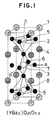
- Superconducting materials are constructed in perovskite-like structures as illustrated in Fig.1 in accordance with the present invention.
- the structure comprises cupper atoms 2, an intervening cupper atom 3, oxygen atoms 5 and 6 surrounding the cupper atoms, oxygen vacancies 7, atoms 1 belonging to Group IIIa of the periodic table such as Y, and atoms 4 belonging to Group IIa such as Ba.
- the superconduction in such a structure may be explained on the grounds that electron pairs are drifted along the layer planes of the layered structures consisting of the oxygen atoms 5 and the central cupper atoms 2 (the plane made of a and b axes, i.e. the c plane) by virtue of the interaction between the oxygen and cupper atoms.
- magnon is regarded to function as a key quasi-particle which allow electron pairs to pass along the layered structure.
- the respective crystalline axes of grains can be aligned by applying an external magnetic field to thin films, preferably while being heated, during formation or after completion of the formation, whereas interaction of magnon or the magnetic substance undergoes, and therefore single crystals can be easily producted at low temperatures.
- the critical current densities along the c plane are larger than those normal to the c plane by two or much orders of magnitude. Because of this, it is very important to align crystalline directions even for fabricating polycrystalline thin films.
- the present invention is effective when applied to deposition of oxide ceramics prepared by mixing oxides of constituents of superconducting materials followed by firing the same, the depostion being carried out by sputtering, electron ion beam evaporation, ion plating, chemical vapor deposition and the like, each carried out at negative pressures, or by spraying, screen press printing and the like, each carried out at air pressure.
- the magnetic field can be applied to a surface on which depostion takes place by inducing the magnetic field at a distant site and introducing the effect of the magnetic field to the surface by means of a magnetic circuit made of a magnetic substance such as nickel or iron.
- A is one or more elements of Group IIIa of the Periodic Table, e.g., the rare earth elements
- B is one or more elements of Group IIa of the Periodic Table, e.g., the alkaline earth metals including beryllium and magnesium, and 0 ⁇ x ⁇ 1
- y 2.0 - 4.0, preferably 2.5 - 3.5
- z 1.0 - 4.0, preferably 1.5 - 3.5
- w 4.0 - 10.0, preferably 6.0 - 8.0.
- the high purity chemicals were pressed in a capsule at 100Kg/cm and formed into a cylindrical shaped tablet of 25 mm diameter and 3 mm height.
- the tablet was heated (fired) and oxidized at 500-1400°C, e.g., 950°C for 8 hours in an oxdizing atmosphere such as in air, this step being called pre-firing hereinafter.
- Fig. 2 is a schematic diagram showing an apparatus for manufacturing superconducting films in accordance with the present invention.
- the apparatus comprises a vacuum chamber 41, an evacuation system 25, a gas introducing system 40 having three branchs 32, 33 and 34, a target holding structure 10, a substrate holder 31, a magnetic circuit comprising a magnetic potential source 26, one of magnetic poles 27 just behind the substrate holder 31 and the other magnetic pole 14 just behind a backing plate 13 of the holding structure 10 on which a target 12 is mounted.
- the holding structure is supplied with a high negative voltage 20 by means of a voltage source and cooled with cooling water circulated through an inlet port 15 and an outlet port 15′.
- the structure 10 is isolated from the chamber 41 by a Teflon insulator 18. The periphery of the sturcture is protected by a shield plate 17.
- the substrate holder 31 is provided with a heater 29 in order to heat a substrate 30 on which deposition is carried out by sputtering.
- the magnetic field 28 induced between the structure 10 and the holder 31 is controlled by means of the potential source 26.
- the locations of the holding structure 10 and the substrate holder 31 are such that the distance between the substrate 30 and the target 12 is 2-15 cm.
- the evacuation system 25 comprises a turbo molecular pump 21, a pressure control valve 22 and a rotary pump 23.
- Ceramic tablets fired as described supra is mounted on the structure 10 as a sputtering target 12 in the form in correspondence with the structure of thin films to be deposited on the substrate 30.
- the crystalline directions of the tablets is aligned with those of the thin films to be deposited, so that the crystallinity of the laminate thin film is enhanced.
- the magnetic field induced between the target 12 and substrate 30 is controlled by the potential source 26 to be not weeker than 0.3 T, e.g. 0.5 T. Stronger magnetic fields are preferable in general.
- argon, oxygen and a halogen compound gas such as NF3 are introduced into the chamber 41 at appropriate pressures through the branchs 32, 33 and 34 of the introduction system 40 respectively.
- a high voltage electric power inputted to the target holder 16 the target 12 is sputtered and deposited on the substrate 30 in a magnetic field.
- a target 12 of 25 mm diameter was prepared in consistence with the stoichiometric composition YBa2Cu 3.8 O6 ⁇ 8.
- the distance between the target and the substrate was 3 cm.
- the pressure of argon in the chamber was 4 x 10 ⁇ 1Pa.
- the oxygen amount introduced was 20% of the argon amount.
- the input power for DC sputtering was 500W.
- the magnetic field strength was 0.2 T at the substrate surface.
- the substrate 30 was heated to 750°C and rotated during deposition around its axis parallel to the direction of magnetic field in order to perform deposition uniformly. In this deposition condition, ceramic films of 0.5 to 3 microns thickness were deposited at 5-100 ⁇ /min, e.g. 50 ⁇ /min.
- the ceramic films were annealed at 850°C for 3 hours in an oxygen atmosphere (at air pressure). followed by gradually cooling and anealing at 350-500°C for two hours.
- superconducting oxide ceramic films were obtained which have a modified perovskite-like structure of orthorhobic system.
- the Tco was measured to be 98K.
- the critical current density was measured to be 3 x 10 ⁇ 4 A/cm2.
- the (a,b) planes of the target 12 and the film 50 were normal to the plane of the drawing sheet.
- Example 1 The procedure of Example 1 was repeated with the exception as follow. Particularly, the substrate holder as illustrated in Fig.3 was employed in place of that illustrated in Fig.2. The holder carries a pair of magnet poles 14 and 27 between which a magnetic field parallel to the substrate 30 is induced as depicted with arrow 28. A target 12 of 25 m m diameter was prepared in consistence with the stoichiometric composition Y 0.5 Yb 0.5 Ba SrCu 3.606-8. The (a,b) planes of the target 12 and the film 50 were chosen normal to the planes of the backing plate 13 and the substrate 31.
- the substrate 30 was made of glass, alumina or ZrO2 and coated with a platinum electrode by sputtering at 500°C.
- a superconducing film 50 was deposited on the platinum electrode followed by coating with a gold electrode.
- the Tc was measured to be 93°C.
- the critical current density between the platinum and gold electrodes was measured to be 2.4 x 10⁴ A/cm2. When the critical current density was measured with reference to current passing through parallel to the film, it was only 1 x 10³ A/cm2.
- Example 1 The procedure of Example 1 was repeated with the exception specified below. Particularly, a MgO substrate of (100) plane or a SrTiO3 substrate of (110) plane was employed in place of the substrate 31. The magnetic field was 1.5 T at the substrate surface. As a result, single-crystalline thin films having 1.5 microns thickness and 1 cm2 or larger area were formed.
- Example 2 Substantially same procedure as in Example 2 was repeated with exception specified below. Particularly, a MgO substrate of (110) plane or a SrTiO3 substrate (110) was employed in place of the substrate 31. The magnetic field was 1.5 T at the substrate surface. As a result, single-crystalline thin films having 1.5 microns thickness and a surface area as broad as 5 mm2 were formed.
- the apparatus comprises a vacuum chamber 41, an evacuation system 25, a gas introducing system 40 (only an inlet conduit is shown), a magnetic circuit comprising a magnetic potential source 26, one of magnetic poles 27 and the other magnetic pole 27′, melting pots 55, a substrate holder 31 and a magnetic circuit 27.
- the apparatus is further provided with an electron beam emitting device.
- the substrate holder 31 is provided with a heater 29 in order to heat a substrate 30 on which deposition is carried out by evaporation.
- a magnetic field is induced across the substrate 30 by means of magnets 27 and 27′ and its strength is controlled by means of the potential source 26.
- the evacuation system 25 comprises a turbo molecular pump 21, a pressure control valve 22 and a rotary pump 23.
- the pots 51, 52 and 53 retain ittrium or its compound, cupper or its compound and barrium or its compound respectively.
- Evaporation deposition was carried out in a conventional manner with the exception that the deposited material was subjected to a magnetic field during deposition as depicted with arrow 28.
- the critical current density was measured to be 1.5 x 10⁴ A/cm2.
- the Tc and Tc onset were 94K and 97K respectively.
- the manufacturing process was repeated again making no use of magnetic field.
- the critical current density was only on the order of 102 A/cm2.
- Examples of this general formula are BiSrCaCuCu2O x and Bi4Sr3Ca3Cu4O x .
- Tc onset and Tco samples in consistent with the formula Bi4Sr y Ca3Cu4O x (y is around 1.5) were measured to be 40-60°K, which is not so high.
- Relatively high critical temperatuers were obtained with samples conforming to the stoichiometric formulae Bi4Sr4Ca2Cu4O x and Bi2Sr3Ca2Cu2O x .
- the number x denoting the oxygen proportion is 6-10, e.g. around 8.1.
- Such superconducting materials can be formed by screen press printing, vacuum evaporation or CVD.
- Groups Ia, IIa, VIII, Ib, IIb and 0 are the same in the Japanese and European Periodic Tables
- Groups IIIa, IVa, Va, VIA and VIIa of the Japanese Period Table correspond respectively to Groups IIIb, IVb, Vb, VIb and VIIb of the European Periodic Table
- Groups IIIb, IVb, Vb, VIb and VIIb of the Japanese Periodic Table correspond respectively to Groups IIIa, IVa, Va, VIa and VIIa of the European Periodic Table.
Landscapes
- Engineering & Computer Science (AREA)
- Manufacturing & Machinery (AREA)
- Superconductors And Manufacturing Methods Therefor (AREA)
- Inorganic Compounds Of Heavy Metals (AREA)
- Superconductor Devices And Manufacturing Methods Thereof (AREA)
- Physical Vapour Deposition (AREA)
- Compositions Of Oxide Ceramics (AREA)
Applications Claiming Priority (7)
| Application Number | Priority Date | Filing Date | Title |
|---|---|---|---|
| JP218535/87 | 1987-08-31 | ||
| JP218537/87 | 1987-08-31 | ||
| JP62218536A JPS6460925A (en) | 1987-08-31 | 1987-08-31 | Fabricating method for superconductive material |
| JP62218537A JPS6459974A (en) | 1987-08-31 | 1987-08-31 | Device for manufacturing superconducting material |
| JP62218535A JP2564562B2 (ja) | 1987-08-31 | 1987-08-31 | 超電導材料の作製方法 |
| JP218536/87 | 1987-08-31 | ||
| JP3094817A JPH05279025A (ja) | 1987-08-31 | 1991-04-01 | 酸化物超電導薄膜 |
Publications (3)
| Publication Number | Publication Date |
|---|---|
| EP0306286A2 true EP0306286A2 (de) | 1989-03-08 |
| EP0306286A3 EP0306286A3 (en) | 1989-05-03 |
| EP0306286B1 EP0306286B1 (de) | 1996-07-03 |
Family
ID=27468264
Family Applications (1)
| Application Number | Title | Priority Date | Filing Date |
|---|---|---|---|
| EP88308047A Expired - Lifetime EP0306286B1 (de) | 1987-08-31 | 1988-08-31 | Methode und Gerät zur Herstellung von supraleitenden keramischen Materialien |
Country Status (4)
| Country | Link |
|---|---|
| EP (1) | EP0306286B1 (de) |
| KR (1) | KR920007799B1 (de) |
| CN (1) | CN1016387B (de) |
| DE (1) | DE3855391T2 (de) |
Cited By (6)
| Publication number | Priority date | Publication date | Assignee | Title |
|---|---|---|---|---|
| EP0313996A3 (de) * | 1987-10-28 | 1989-07-26 | Hoechst Aktiengesellschaft | Dünner supraleitender Film, seine Herstellung und Verwendung |
| EP0367571A3 (en) * | 1988-11-02 | 1990-08-01 | Hitachi Chemical Company Ltd. | Superconducting thick film circuit board, production thereof, thick film superconductor and production thereof |
| EP0310332A3 (de) * | 1987-09-28 | 1990-11-14 | Arch Development Corporation | Bevorzugte Orientierung von supraleitenden Metalloxidmaterialien |
| EP0377566A4 (en) * | 1987-09-16 | 1990-12-27 | Dominic J. Giancola | Process embodiments for improving the electrical properties of conductors |
| WO2001014610A3 (de) * | 1999-08-25 | 2001-05-10 | Nanogate Gmbh | Verfahren zur veränderung von beschichtungsmaterialien |
| CN112553681A (zh) * | 2020-11-21 | 2021-03-26 | 嘉兴固美科技有限公司 | 一种大块体单晶铜的制备方法 |
Families Citing this family (1)
| Publication number | Priority date | Publication date | Assignee | Title |
|---|---|---|---|---|
| CN101177775B (zh) * | 2006-11-10 | 2010-09-15 | 中国科学院物理研究所 | 具有外加磁场的真空淀积薄膜和薄膜热处理设备 |
Family Cites Families (1)
| Publication number | Priority date | Publication date | Assignee | Title |
|---|---|---|---|---|
| AU600345B2 (en) * | 1987-03-23 | 1990-08-09 | Semiconductor Energy Laboratory Co. Ltd. | Method of manufacturing superconducting ceramics under a magnetic field |
-
1988
- 1988-08-31 EP EP88308047A patent/EP0306286B1/de not_active Expired - Lifetime
- 1988-08-31 CN CN88106462A patent/CN1016387B/zh not_active Expired
- 1988-08-31 KR KR1019880011107A patent/KR920007799B1/ko not_active Expired
- 1988-08-31 DE DE3855391T patent/DE3855391T2/de not_active Expired - Fee Related
Cited By (7)
| Publication number | Priority date | Publication date | Assignee | Title |
|---|---|---|---|---|
| EP0377566A4 (en) * | 1987-09-16 | 1990-12-27 | Dominic J. Giancola | Process embodiments for improving the electrical properties of conductors |
| EP0310332A3 (de) * | 1987-09-28 | 1990-11-14 | Arch Development Corporation | Bevorzugte Orientierung von supraleitenden Metalloxidmaterialien |
| EP0313996A3 (de) * | 1987-10-28 | 1989-07-26 | Hoechst Aktiengesellschaft | Dünner supraleitender Film, seine Herstellung und Verwendung |
| EP0367571A3 (en) * | 1988-11-02 | 1990-08-01 | Hitachi Chemical Company Ltd. | Superconducting thick film circuit board, production thereof, thick film superconductor and production thereof |
| WO2001014610A3 (de) * | 1999-08-25 | 2001-05-10 | Nanogate Gmbh | Verfahren zur veränderung von beschichtungsmaterialien |
| CN112553681A (zh) * | 2020-11-21 | 2021-03-26 | 嘉兴固美科技有限公司 | 一种大块体单晶铜的制备方法 |
| CN112553681B (zh) * | 2020-11-21 | 2021-10-08 | 嘉兴固美科技有限公司 | 一种大块体单晶铜的制备方法 |
Also Published As
| Publication number | Publication date |
|---|---|
| CN1016387B (zh) | 1992-04-22 |
| DE3855391D1 (de) | 1996-08-08 |
| DE3855391T2 (de) | 1997-02-13 |
| KR920007799B1 (ko) | 1992-09-17 |
| EP0306286B1 (de) | 1996-07-03 |
| KR890004454A (ko) | 1989-04-22 |
| CN1031773A (zh) | 1989-03-15 |
| EP0306286A3 (en) | 1989-05-03 |
Similar Documents
| Publication | Publication Date | Title |
|---|---|---|
| US4963524A (en) | Sputtering device for manufacturing superconducting oxide material and method therefor | |
| Lichtenberg et al. | Sr2RuO4: A metallic substrate for the epitaxial growth of YBa2Cu3O7− δ | |
| CA1330548C (en) | Method and apparatus for producing thin film of compound having large area | |
| KR0132061B1 (ko) | 초전도 박막의 제작 방법 | |
| JP2671916B2 (ja) | 超電導体の製造方法及び超電導回路の作製方法 | |
| EP0306286A2 (de) | Methode und Gerät zur Herstellung von supraleitenden keramischen Materialien | |
| US5126318A (en) | Sputtering method for forming superconductive films using water vapor addition | |
| Yu et al. | HgBa2CaCu2Oy superconducting thin films prepared by laser ablation | |
| US5225396A (en) | Method for forming an oxide superconducting film | |
| JPH0825742B2 (ja) | 超電導材料の作製方法 | |
| JP2713343B2 (ja) | 超電導回路の作製方法 | |
| Truman et al. | Continued improvement of large area, in situ sputter deposition of superconducting YBCO thin films | |
| JP2564562B2 (ja) | 超電導材料の作製方法 | |
| JP2603688B2 (ja) | 超電導材料の改質方法 | |
| JP2502344B2 (ja) | 複合酸化物超電導体薄膜の作製方法 | |
| JP2529347B2 (ja) | 超電導薄膜の作製方法 | |
| JPH0764678B2 (ja) | 超電導薄膜の作製方法 | |
| JP2683689B2 (ja) | 酸化物超伝導薄膜作製方法 | |
| JP3163651B2 (ja) | 超電導薄膜の成膜方法と装置 | |
| JP2668532B2 (ja) | 超電導薄膜の作製方法 | |
| JP2639510B2 (ja) | 超電導薄膜の作製方法 | |
| JP2557446B2 (ja) | 複合酸化物系超電導薄膜の製造方法 | |
| JP2525852B2 (ja) | 超電導薄膜の作製方法 | |
| Chae et al. | Preparation of cathodic arc deposited HTSC Bi/sub 2/Sr/sub 2/CaCu/sub 2/O/sub 8+ y/-Ag composite thin films on Ag substrates | |
| Lin et al. | Large-area growth of superconducting Y-Ba-Cu-O films by hot-wall sputtering method |
Legal Events
| Date | Code | Title | Description |
|---|---|---|---|
| PUAI | Public reference made under article 153(3) epc to a published international application that has entered the european phase |
Free format text: ORIGINAL CODE: 0009012 |
|
| AK | Designated contracting states |
Kind code of ref document: A2 Designated state(s): DE FR GB |
|
| PUAL | Search report despatched |
Free format text: ORIGINAL CODE: 0009013 |
|
| AK | Designated contracting states |
Kind code of ref document: A3 Designated state(s): DE FR GB |
|
| 17P | Request for examination filed |
Effective date: 19890531 |
|
| 17Q | First examination report despatched |
Effective date: 19910429 |
|
| GRAH | Despatch of communication of intention to grant a patent |
Free format text: ORIGINAL CODE: EPIDOS IGRA |
|
| GRAH | Despatch of communication of intention to grant a patent |
Free format text: ORIGINAL CODE: EPIDOS IGRA |
|
| GRAA | (expected) grant |
Free format text: ORIGINAL CODE: 0009210 |
|
| AK | Designated contracting states |
Kind code of ref document: B1 Designated state(s): DE FR GB |
|
| REF | Corresponds to: |
Ref document number: 3855391 Country of ref document: DE Date of ref document: 19960808 |
|
| PGFP | Annual fee paid to national office [announced via postgrant information from national office to epo] |
Ref country code: FR Payment date: 19960809 Year of fee payment: 9 |
|
| PGFP | Annual fee paid to national office [announced via postgrant information from national office to epo] |
Ref country code: GB Payment date: 19960822 Year of fee payment: 9 |
|
| PGFP | Annual fee paid to national office [announced via postgrant information from national office to epo] |
Ref country code: DE Payment date: 19960906 Year of fee payment: 9 |
|
| ET | Fr: translation filed | ||
| ET | Fr: translation filed | ||
| PLBE | No opposition filed within time limit |
Free format text: ORIGINAL CODE: 0009261 |
|
| STAA | Information on the status of an ep patent application or granted ep patent |
Free format text: STATUS: NO OPPOSITION FILED WITHIN TIME LIMIT |
|
| 26N | No opposition filed | ||
| PG25 | Lapsed in a contracting state [announced via postgrant information from national office to epo] |
Ref country code: GB Free format text: LAPSE BECAUSE OF NON-PAYMENT OF DUE FEES Effective date: 19970831 |
|
| GBPC | Gb: european patent ceased through non-payment of renewal fee |
Effective date: 19970831 |
|
| PG25 | Lapsed in a contracting state [announced via postgrant information from national office to epo] |
Ref country code: FR Free format text: LAPSE BECAUSE OF NON-PAYMENT OF DUE FEES Effective date: 19980430 |
|
| PG25 | Lapsed in a contracting state [announced via postgrant information from national office to epo] |
Ref country code: DE Free format text: LAPSE BECAUSE OF NON-PAYMENT OF DUE FEES Effective date: 19980501 |
|
| REG | Reference to a national code |
Ref country code: FR Ref legal event code: ST |