EP0306533A1 - Schnelles betriebssystem mit schwebendem punkt - Google Patents
Schnelles betriebssystem mit schwebendem punkt Download PDFInfo
- Publication number
- EP0306533A1 EP0306533A1 EP19880901641 EP88901641A EP0306533A1 EP 0306533 A1 EP0306533 A1 EP 0306533A1 EP 19880901641 EP19880901641 EP 19880901641 EP 88901641 A EP88901641 A EP 88901641A EP 0306533 A1 EP0306533 A1 EP 0306533A1
- Authority
- EP
- European Patent Office
- Prior art keywords
- calculation
- host processor
- data
- floating point
- command
- Prior art date
- Legal status (The legal status is an assumption and is not a legal conclusion. Google has not performed a legal analysis and makes no representation as to the accuracy of the status listed.)
- Withdrawn
Links
Images


Classifications
-
- G—PHYSICS
- G06—COMPUTING OR CALCULATING; COUNTING
- G06F—ELECTRIC DIGITAL DATA PROCESSING
- G06F9/00—Arrangements for program control, e.g. control units
- G06F9/06—Arrangements for program control, e.g. control units using stored programs, i.e. using an internal store of processing equipment to receive or retain programs
- G06F9/30—Arrangements for executing machine instructions, e.g. instruction decode
- G06F9/38—Concurrent instruction execution, e.g. pipeline or look ahead
- G06F9/3885—Concurrent instruction execution, e.g. pipeline or look ahead using a plurality of independent parallel functional units
-
- G—PHYSICS
- G06—COMPUTING OR CALCULATING; COUNTING
- G06F—ELECTRIC DIGITAL DATA PROCESSING
- G06F9/00—Arrangements for program control, e.g. control units
- G06F9/06—Arrangements for program control, e.g. control units using stored programs, i.e. using an internal store of processing equipment to receive or retain programs
- G06F9/30—Arrangements for executing machine instructions, e.g. instruction decode
- G06F9/38—Concurrent instruction execution, e.g. pipeline or look ahead
- G06F9/3877—Concurrent instruction execution, e.g. pipeline or look ahead using a secondary processor, e.g. coprocessor
- G06F9/3879—Concurrent instruction execution, e.g. pipeline or look ahead using a secondary processor, e.g. coprocessor for non-native instruction execution, e.g. executing a command; for Java instruction set
Definitions
- the present invention relates to a fast floating point calculation system.
- FFP fast floating point processors
- a fast floating point calculation system is constructed wherein a host processor, which is made up of a general purpose processor or processors, supplies the FFP with command blocks which include data needed for calculation and commands the FFP to execute calculation; the FFP comprises a data storing portion which stores the supplied command blocks, and a calculation executing portion which executes the calculations in accordance with the command blocks stored in the data storing portion and again stores the calculation result in the data storing portion. And when a calculation results is stored in the data storing portion, the host processor reads that result.
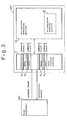
- FIG. 1 shows an example of the hardware construction for the system as mentioned above.
- reference numeral 100 is a fast floating point processor (FFP), and 200 is a host processor, and these are connected through a back plane bus 70 and a bus interface 71.
- the construction of the fast floating point processor (FFP) 100 is as described hereinafter.
- Reference numeral 3 is a data storing portion
- 4 is a calculating portion
- 5-1 is a microprogram controlling portion
- 5-2 is a clock generating portion
- 9 is a two-way buffer.
- the microprogram controlling portion 5-1 comprises a microprogram storing portion 52 (hereinafter called Writable Control Storage, or WCS), in which a microprogram is written in advance, and the microprogram controlling portion 5-1 controls the data storing portion 3 and the calculating portion 4 in accordance with the microprogram.
- WCS Writable Control Storage
- the calculating portion 4 reads the data for calculation from the data storing portion 3 under the control of the microprogram controlling portion 5-1 and executes calculation, and writes the calculation results again in the data storing portion 3.
- the data storing portion 3 comprises a data RAM 30, a R/W (read/write) control circuit 31, an address generator 33, an address register 33, and a register 34.
- the data for calculation sent through the two-way buffer 9 and data bus 73 from the host processor 200 is temporarily written in the data RAM 30, and next the data for calculation is read out therefrom.
- the calculation results of the calculating portion 4 are written again in the data RAM 30, and read out by the host processor 200.
- the R/W control circuit 31 outputs an output enable signal or a write enable signal to the data RAM 30, under the control of the microprogram controlling portion 5-1 (shown by a symbol "M" in Fig.
- R/W control circuit 31 An example of construction of the R/W control circuit 31 is shown in Fig. 2.
- the address generator 32 outputs an address of the data RAM 30 under the control of the microprogram controlling portion 5-1 in the case of data transfer between the data RAM 30 and the calculating portion 4.
- the addressing in the case of data transfer between the host processor 200 and the data RAM 30 is-carried out through the address register 33.
- the register 34 is provided for transferring data from the data RAM 30 to the microprogram controlling portion 5-1, or to the address generator 32.
- the clock generating portion 5-2 comprises a clock generator 54 and a clock control portion 55. Clock pulses generated at the clock generator 54 are output through the clock control portion 55, and synchronize the microprogram controlling portion 5-1 and all portions controlled by the microprogram controlling portion 5-1 in the FFP.
- the two-way buffer 9 is made by connecting two buffers in parallel with each other, one of which is used for transferring data from the host computer 200 to the data RAM 30, and the other'of which is used for transferring data in the opposite direction as shown in Fig. 1. Both buffers are usually in the high-impedance state, and the host computer 200 and the data RAM 30 are electrically isolated. Each of the buffers is made ON by the host processor 200, and enables data transfer.
- An object of the present invention is to make it possible for a host processor to supply commands for the following calculations successively, even during the execution of calculation in the fast floating point processor, and make it possible for the fast floating point processor to start the calculation for the next command block when the calculation for the preceding command block is completed, and consequently, to realize a higher execution speed overall.
- the host processor commands the fast floating point processor to execute a calculation by supplying a command block which contains data needed for the calculation;
- the fast floating point processor comprises a data storing portion which stores the supplied command block, and a calculation executing portion which executes the calculation in accordance with the command block stored in the data storing portion, and stores the calculation result in the data storing portion;
- the host processor reads the calculation result stored in the data storing portion; wherein each of a plurality of the command blocks is stored in the region addressed by the host processor in the data storing portion, and each of the command blocks contains information showing an address of the region in the data storing portion where the command block to be processed next is stored, and the calculation executing portion successively executes the calculations for the plurality of the command blocks which are stored in advance, with referrence to the information.
- each of a plurality of the command blocks from a host processor 200 is stored in the region addressed by the host processor 200 in the data storing portion 3 in a FFP 100, and each of the command blocks contains an information A 1 , A z , A 3 , A4, ⁇ showing an address of the region in the data storing portion where the command block to be processed next is stored.
- Figure 4 shows a first example of the hardware construction of the fast floating point calculation system according to the present invention.
- the hardware construction of Fig. 4 is the same as the hardware construction of the Fig. 1, except for the status register 8 provided in Fig. 4.
- the status register 8 consists of a group of flags each of which is provided for the corresponding one of a plurality of command blocks which are stored in the data RAM 30, to indicate whether or not the calculation is completed and the calculation result is stored in the data RAM 30.
- each of the command blocks transferred from the host processor to the FFP 100 in the first and second embodiments of the present invention contains an identifying number "CB No.” for discriminating among the command blocks stored in the data RAM 30 at the same time, and the flag provided for each command block corresponds to the "CB No.”
- Each flag is set in the state "1" when the corresponding command block is written by the host processor 200, and is set in the state "0" when the calculation result is read by the host processor 200.
- FIG. 5 shows an example of the format of command block (hereinafter called CB) and the chaining in the fast floating point calculation system according to the present invention.
- CB command block
- Fig. 5 the most significant bit (MSB) of the top address in each command block is shown as "V”. If this bit is "1”, it means that the following command block is to command to execute a calculation, and if the bit is "0”, it means that the calculation is completed.
- MSB most significant bit
- Fig. 5 is a abbreviation of "instruction”, and this part shows a function to be fulfilled according to the command block. Concretely, that is a top address of the microprogram corresponding to the function.
- CB No. is an identifying number "CB No.” for discriminating among the command blocks stored in the data RAM 30 at the same time.
- NXT CB POINTER corresponds to "the information showing an address of the region in the data storing portion where the command block to be processed next is stored" according to the present invention and as mentioned before.
- CB POINTER is a register to load the top address of the region in the data storing portion, at which the command block is stored for which the execution of the FFP is carried out at that time.
- one register A (not shown) in the address register 32 is used for that purpose. Therefore, "NEXT CB POINTER” indicates the top address of the region in the data storing portion 3, at which the command block is stored for which command block the execution of the FFP.to be carried out next.
- the region at which each of the command blocks is stored can be located arbitrarily unless the regions of the command blocks overlap each other or the other memory region, and the locations of the command blocks are determined by the host processor 200.
- Figure 6 shows an execution process of the host processor 200 in the fast floating point calculating system as an embodiment of the present invention.
- step 302 the contents of the microprogram storing portion (WCS) 52 (in the hardware construction of Fig. 4) and the data RAM 30 are initialized, and in step 303, a count of the command blocks (a count value which indicates the number of command blocks supplied to the FFP but for which the corresponding calculation result has not been read out) is set to zero.
- WCS microprogram storing portion
- step 304 it is determined whether or not there is a prepared command block to be supplied to the FFP, to make the FFP execute the calculation. If N0, the program jumps to steps (309 -312) for reading out the calculation results, but a prepared command block is to be supplied to the FFP, the program jumps to step 305, and it is determined whether the number of command blocks supplied to the FFP, but for which the corresponding calculation result has not been read out, has reached the maximum number of command blocks that can be stored in that FFP at the same time. (The maximum number is shown as eight in the example of Fig. 6, although, since in the example of Fig.
- MSB of the top address i.e., "V"
- step 308 the "V” in the command block in the abovementioned step 306 is set to "1", and the count of the command blocks is incremented.
- step 309 it is determined whether or not the content of the status register (described later)-in the FFP is "1".
- the status register in the FFP as mentioned before in the description of Fig. 4, consists of a group of flags, each of which is provided for the corresponding one of the "CB Nos.”.
- the FFP stores the result in the predetermined region in the data storing portion (data RAM 30), and then sets the corresponding flag in the status register in the state "1". If no flag is in the state "1", a calculation result has not been obtained yet in the FFP, and therefore, the program jumps again to steps 304-308 for writing data.
- step 304 If any bit in the status register is in the state "1", the calculation result of the command block corresponding to that bit is read from the data RAM 30 in step 310, and then the bit in the status register corresponding to the read out calculation result is cleared to zero in step 311. In step 312, the CB count is decremented corresponding to the reading of the one calculation result, and thus room for the input of a new command block is generated. The program then, jumps to step 304.
- FIG. 7 shows an execution process of the fast floating point processor (FFP) 100.
- FFP fast floating point processor
- Step 407 corresponds to the execution of the fast floating point calculation in the FFP, and in step 407, the FFP executes the calculation using the data in the data region in the command block as parameters, and stores the calculation result in the data region of the command block.
- step 408 as mentioned before in the explanation of Fig. 6, the FFP sets the bit in the status register corresponding to the "CB No.” in the command block in which the calculation result is stored in the state "1", i.e., the FFP shows that the calculation result in the command block can be read.
- step 409 the FFP reads the "NEXT CB POINTER" in the above command block and stores the top address of the region in the data RAW at which the next command block is stored, in the aforementioned CB pointer (the register A in the address generator 32), and then proceeds to step 403 for the execution for the next command block.
- the host processor can supply the following commands successively even during the execution of a calculation by the FFP, and thus the FFP can start the execution of a calculation for the next command block immediately after the execution of the calculation for the preceding command block is completed.
- Fig. 8A the connection to the host processor 200 through the back plane bus 70 and the bus interface 71, the construction and the function of the data storing portion 3 and the clock generating portion 5-2, and the function of the microprogram controlling portion 5-1, the calculating portion 4, and the status register 8, are the same as in the FFP in Fig. 1. More details of the internal construction of the microprogram controlling portion 5-1 and the calculating portion 4 are shown in Fig. 8A. As the detailed internal construction of the microprogram controlling portion 5-1 and the calculating portion 4 does not directly relate to the present invention, it is briefly explained hereinafter.
- the calculating portion 4 comprises a register file 40, a floating point multiplier/divider (MPY/DIV) 41, and a floating point arithmetic logic unit (ALU) 42.
- MPY/DIV floating point multiplier/divider
- ALU floating point arithmetic logic unit
- the register file 40 reads data for calculation from the data RAM 30, and supplies the data to the MPY/DIV 41, under the control of the microprogram controlling portion 5-1, or holds the data during the calculation and the final calculation result therein.
- the final calculation result is written in the data RAM 30 from the register file 40.
- the ALU 42 executes addition/subtraction calculations and comparison/logic calculations
- the MPY/DIV 41 executes multiplication/division calculations.
- Each of the ALU 42 and the MPY/DIV 41 has two kinds of outputs, respectively. One is the output of the results of arithmetic calculations such as the addition/subtraction calculations or multiplication/div ision calculations, and these results of arithmetic calculations are input to the register file 40.
- the other output from each of the ALU 42 and the MPY/DIV 41 comprises status signals showing the results of the comparison/logic calculations or the occurence of errors during the calculations.
- the microprogram controlling portion 5-1 decodes the status signal and determines the microinstruction to be executed next.
- the microprogram controlling portion 5-1 comprises a sequential control circuit 51, the aforementioned WCS , a microcode register 53, a decoder 56, an error memorizing portion 57, a multiplexer 58, and a register 59.
- the WCS consists of a RAM, and a microprogram from the host processor 200 is written in the WCS 52 at the beginning of the execution of the FFP.
- a WCS writing control portion 60 receives a request for writing of a program from the host processor 200, it holds the sequential control circuit 51 at the initial state by applying a CLEAR signal output to the sequential control circuit 51, and opens a buffer gate 61.
- WCS addresses and WCS data (microinstruction) from the host processor 200 are input to the WCS 52 through the two gates of the buffer gate 61.
- the sequential control circuit 51 When the sequential control circuit 51 outputs the address of the WCS 52, a microinstruction stored at the address is loaded in the microcode register 53, and the microinstruction is executed.
- the status signals from the calculating portion 4 are decoded through a decoder, the error memorizing portion 57, and the multipler 58, and the contents of the status signals are loaded in the register 59 in turn.
- the sequential control circuit 51 outputs the next address based on the content of the register 59.
- the microprogram controlling portion 5-1 operates as mentioned above.
- FIG. 8B The construction of the two-way buffer register 1 is shown in Figure 8B.
- reference numerals 11, 12 are registers to which applied data are written under the control (a signal WP1 and WP2) of the controlling portion for assisting access by host processor 2
- reference numerals 13, 14 are (tri-state, or three-state) buffers which output data under the control (a signal OE1 and OE2) of the controlling portion for assisting access by host processor 2.
- FIG. 8C The construction of the controlling portion for assisting access by host processor 2 is shown in Figure 8C.
- reference numerals 21, 22, 23 are D flip-flop circuits, 24, 25, 27, 29 are AND circuits, and 26, 28 are NAND circuits.
- Figures 9A and 9B show the timing of the controlling portion for assisting access by the host processor 2.
- Figure 9A shows the timing when reading data in the data RAM 30 to the host processor 200.
- a strobe signal (STB) and a read/write (R/W) signal are input to the controlling portion for assisting access by the host processor 2 from the host processor 200 through the bus interface 71.
- These signals are input to the R/W control circuit 31 through the bus interface 71 in the conventional construction of Fig. 1 (Fig. 2).
- the R/W signal is always in the state "0" at the time of writing data, and always in the state "1" at the time of reading data.
- Fig. 9A when the R/W signal is in the state "0", the outputs are "HOST", "WP1". and "OE1'.
- the HOST is input to the clock controlling portion 55 in Fig. 8A, and stops the clock pulses which synchronize the FFP.
- the WP1 is applied as a trigger input of the register 11 in the two-way buffer register 1, as shown in Fig. 8B.
- Fig. 9A at the timing of leading edge of the WPl, the data transferred from the data RAM 30 is set in the register 11.
- Another output OE1 is applied as a control input of a (tri-state, or three-state) buffer 13 in the two-way buffer register 1 in Fig. 8B.
- the data loaded in the register 11 after the data is set in the register 11 and before the strobe signal becomes "0" is read by the host processor 200.
- the above HOST signal, and an OE2 signal which is an inversion of an OE2 signal are input to the R/W control circuit 31 instead of the strobe signal and the R/W signal. Since the OE2 is "0" when reading data, the data is read, as understood by Fig. 2, from the R/W control circuit 31 when the above HOST signal becomes "1", i.e., when the WP1 becomes . 0". This data is set in the register 11.
- the HOST When the data is set in the register 11, the HOST returns to "0", and therefore, the stop control of the clock pulses of the clock control portion 55 is stopped, i.e., the stop of the clock pulses is released when the setting data in the register 11 is completed.
- the stop time of the clock pulse is one cycle time of the clock pulse in the FFP.
- the HOST signal plays the same role as in the case of Fig. 9A.
- the output WP2 is applied as a trigger input of the register 12 in the two-way buffer register 1 as shown in Fig. 8B.
- the OE2 is applied as a control input of the (tri-state) buffer 14 in the two-way buffer register 1, and becomes "1" at the same time as the above HOST signal.
- the signal OE2 is inverted as an OE2 signal and input to the R/W control circuit 31 together with the HOST, and then makes the R/W control circuit 31 output a write enable signal.
- the HOST signal stops the clock pulses which synchronize the FFP, and the HOST signal and the OE2 signal operate on the R/W control circuit 31, and makes the data RAM 30 writable, and further, at the same time, the OE2 opens the (tri-state) buffer 14 in the two-way buffer register 1. Therefore, the data from the host processor 200 is written in the data RAM 30.
- the stop time of the FFP is one cycle time of the clock pulse in the FFP.
- the timing of writing data from the host processor 200 to the data RAM, and the timing of reading data to the host processor 200 is considered in the cases of the FFP having a construction of Fig. 4 (and Fig. 1), and the FFP having a construction of Fig. 8A.
- Figure 10A shows the timing of writing data from the host processor (hereinafter called HP in Figs. 10A and 10B) 200 to the data RAM 30, and reading data from the data RAM 30 to the host processor 200 in the fast floating point processor (FFP) 100 shown Fig. 4.
- the execution cycles in the host processor (HP) 200 are shown in (a)
- the executing time of the calculation amd stop time in the FFP 100 are shown in (b)
- the timing of the clock pulse (CLK) in the FFP 100 is shown in (c) .
- a s indicates a cycle in which the host processor 200 outputs a signal to stop the clock pulse (clock stop signal).
- clock stop signal is input to the clock control portion 55 in the FFP 100
- the clock control portion 55 stops the output of the clock pulse in the FFP (time t 1 ), and thus the execution of the calculation in the FFP 100 is stoped.
- the host processor 200 opens a (tri-state) buffer in the two-way buffer 9 which is directed from the host processor 200 to the data RAM 30, makes the R/W signal "0", and outputs a strobe signal to the R/W control circuit 31, and thus the writing of data from the host processor 200 to the data RAM 30 is begun (time tz).
- a symbol "W" indicates a cycle in which data is written from the host processor 200 to the FFP 100.
- a cycle A e in which the stop of the FFP 100 is released, as the next machine cycle of the host processor 200, is started, and a clock restart signal for releasing the stop of the clock pulse is output from the host processor 200.
- the clock control portion 55 receives the clock restart signal (time t 4 ), and restarts the output of the clock pulse, and thus the FFP 100 restarts the execution of the calculation.
- the timing relationships are the same as in the case mentioned above.
- the only difference between the reading case and the writing case exists in the cycle of reading data from FFP to the host processor, which cycle starts at time t 7 .
- the host processor 200 opens the buffer directed to the host processor 200 in the two-way buffer register 9, makes the R/W signal "1", and applies it to the R/W control circuit 31 together with the strobe (STB) signal.
- the E/W control circuit outputs a data enable signal (OE) to the data RAM 30, and consequently, data is read from the data RAM 30 to the host processor 200.
- OE data enable signal
- the stop time of the FFP 100 is about twice the machine cycle of the host processor 200. In the example of Fig. 1, in practice, this time is about 2 ⁇ sec.
- Figure 10B shows the timing of a data transfer between the host processor 200 and the data RAM 30 in the FFP in the case of Fig. 8A.
- Fig. 10B the execution cycles in the host processor (HP) 200 are shown in (a), the executing time of the calculation and stop time in the FFP are shown in (b), and the timing of the clock pulse (CLK) in the FFP is shown in (c).
- FIG. 10B A w indicates a data writing cycle in the host processor 200, and A R is a data read cycle .
- each of the stop time for data writing and the stop time for data reading is one microcycle of the FFP (0.1 ⁇ sec in this embodiment).
- the hardware construction of Fig. 8A allows a remarkable reduction of the stop time of the FFP when writing data from the host processor 200 to the FFP 100, and when reading the calculation result.
- This is especially advantageous when applying the execution processes executed in the host processor 200 and the FFP 100, using the data structure of the command block explained with reference to Figs. 5, 6, and 7, and the command block having that data structure, because in the above data structure and the execution process, even during execution of the FFP, the following commands can be supplied successively by suitably interupting the execution, and therefore, the stop time of the execution in the FFP due to the interuption can be reduced by a factor of ten.
- a host processor can successively supply commands for the following calculations even during the execution of calculation in the FFP, and the FFP can start the calculation for the next command block immediately when the calculation for the preceding command block is completed, and consequently, a higher overall execution speed can be realized.
- the stop time of the execution when the host processor supplies the FFP with a command block, and when the host processor reads the calculation result from the FFP, is remarkably reduced, and therefore, the FFP can execute calculations for successive command blocks without disturbance by inputs from and outputs to the host processor, and consequently, the overall execution speed is improved.
- the present invention is useful when applied to a system comprising a host processor and a fast floating point processor, which executes a calculation at a high speed when a command of the calculation is given by the host processor, and the calculation result is read by the host processor.
Landscapes
- Engineering & Computer Science (AREA)
- Software Systems (AREA)
- Theoretical Computer Science (AREA)
- Physics & Mathematics (AREA)
- General Engineering & Computer Science (AREA)
- General Physics & Mathematics (AREA)
- Advance Control (AREA)
- Multi Processors (AREA)
Applications Claiming Priority (2)
| Application Number | Priority Date | Filing Date | Title |
|---|---|---|---|
| JP60169/87 | 1987-03-17 | ||
| JP62060169A JPS63226764A (ja) | 1987-03-17 | 1987-03-17 | 高速浮動小数点演算システム |
Publications (1)
| Publication Number | Publication Date |
|---|---|
| EP0306533A1 true EP0306533A1 (de) | 1989-03-15 |
Family
ID=13134392
Family Applications (1)
| Application Number | Title | Priority Date | Filing Date |
|---|---|---|---|
| EP19880901641 Withdrawn EP0306533A1 (de) | 1987-03-17 | 1988-02-15 | Schnelles betriebssystem mit schwebendem punkt |
Country Status (3)
| Country | Link |
|---|---|
| EP (1) | EP0306533A1 (de) |
| JP (1) | JPS63226764A (de) |
| WO (1) | WO1988007238A1 (de) |
Cited By (4)
| Publication number | Priority date | Publication date | Assignee | Title |
|---|---|---|---|---|
| EP0521486A3 (de) * | 1991-07-03 | 1994-03-09 | Hitachi Ltd | |
| EP0780761A3 (de) * | 1995-12-19 | 1997-11-12 | Cirrus Logic, Inc. | Verfahren und Vorrichtung zum Befehlsvorausholen in einem grafischen Verarbeitungsgerät |
| EP0885529A4 (de) * | 1996-03-07 | 1998-12-23 | ||
| EP0871142A3 (de) * | 1997-03-27 | 1999-11-03 | Sony Computer Entertainment Inc. | Datenverarbeitungsgerät und -verfahren |
Families Citing this family (1)
| Publication number | Priority date | Publication date | Assignee | Title |
|---|---|---|---|---|
| GB8928934D0 (en) * | 1989-12-21 | 1990-02-28 | Boc Group Plc | Treatment of birds |
Family Cites Families (1)
| Publication number | Priority date | Publication date | Assignee | Title |
|---|---|---|---|---|
| JPS6019815B2 (ja) * | 1980-02-15 | 1985-05-18 | 日本電気株式会社 | 転送制御方式 |
-
1987
- 1987-03-17 JP JP62060169A patent/JPS63226764A/ja active Pending
-
1988
- 1988-02-15 EP EP19880901641 patent/EP0306533A1/de not_active Withdrawn
- 1988-02-15 WO PCT/JP1988/000146 patent/WO1988007238A1/ja not_active Ceased
Non-Patent Citations (1)
| Title |
|---|
| See references of WO8807238A1 * |
Cited By (9)
| Publication number | Priority date | Publication date | Assignee | Title |
|---|---|---|---|---|
| EP0521486A3 (de) * | 1991-07-03 | 1994-03-09 | Hitachi Ltd | |
| US5530889A (en) * | 1991-07-03 | 1996-06-25 | Hitachi, Ltd. | Hierarchical structure processor having at least one sub-sequencer for executing basic instructions of a macro instruction |
| EP0780761A3 (de) * | 1995-12-19 | 1997-11-12 | Cirrus Logic, Inc. | Verfahren und Vorrichtung zum Befehlsvorausholen in einem grafischen Verarbeitungsgerät |
| US5917505A (en) * | 1995-12-19 | 1999-06-29 | Cirrus Logic, Inc. | Method and apparatus for prefetching a next instruction using display list processing in a graphics processor |
| EP0885529A4 (de) * | 1996-03-07 | 1998-12-23 | ||
| EP0871142A3 (de) * | 1997-03-27 | 1999-11-03 | Sony Computer Entertainment Inc. | Datenverarbeitungsgerät und -verfahren |
| AU730429B2 (en) * | 1997-03-27 | 2001-03-08 | Sony Interactive Entertainment Inc. | Information processing apparatus and information processing method |
| US6219073B1 (en) | 1997-03-27 | 2001-04-17 | Sony Computer Entertainment, Inc. | Apparatus and method for information processing using list with embedded instructions for controlling data transfers between parallel processing units |
| CN1107923C (zh) * | 1997-03-27 | 2003-05-07 | 索尼计算机娱乐公司 | 信息处理装置及信息处理方法 |
Also Published As
| Publication number | Publication date |
|---|---|
| JPS63226764A (ja) | 1988-09-21 |
| WO1988007238A1 (fr) | 1988-09-22 |
Similar Documents
| Publication | Publication Date | Title |
|---|---|---|
| US4896259A (en) | Apparatus for storing modifying data prior to selectively storing data to be modified into a register | |
| JP2539199B2 (ja) | デジタルプロセッサ制御装置 | |
| US4980819A (en) | Mechanism for automatically updating multiple unit register file memories in successive cycles for a pipelined processing system | |
| US4027291A (en) | Access control unit | |
| US4841439A (en) | Method for restarting execution interrupted due to page fault in a data processing system | |
| JPH0414385B2 (de) | ||
| EP0010197B1 (de) | Datenverarbeitungssystem für das Zusammenwirken eines Hauptspeichers mit einem Steuerteil und einem Datenverarbeitungsteil | |
| US4047245A (en) | Indirect memory addressing | |
| US4642757A (en) | Microinstruction controlled arithmetic control unit | |
| EP0306533A1 (de) | Schnelles betriebssystem mit schwebendem punkt | |
| JPH01120660A (ja) | マイクロコンピュータ装置 | |
| US3480917A (en) | Arrangement for transferring between program sequences in a data processor | |
| JPS59116855A (ja) | 制御メモリ機構 | |
| US5819081A (en) | Method of executing a branch instruction of jumping to a subroutine in a pipeline control system | |
| EP0305527A1 (de) | Hochgeschwindigkeits-recheneinheit mit schwebendem punkt | |
| EP0177712B1 (de) | Einrichtung zur maskierten Datenabholung und -modifizierung | |
| JP2595992B2 (ja) | 電子楽器 | |
| JPH0654505B2 (ja) | 並列型演算処理装置 | |
| EP0305530A1 (de) | Hochgeschwindigkeits-recheneinheit mit schwebendem punkt | |
| US4916601A (en) | Means for transferring firmware signals between a control store and a microprocessor means through a reduced number of connections by transfer according to firmware signal function | |
| US5123093A (en) | Operational processor for performing a memory access and an operational process in parallel | |
| JPS61206358A (ja) | 連続デ−タの高速入力制御装置 | |
| JPH113592A (ja) | 同期式ramのアクセス制御回路、データ処理プロセッサ及びその制御方法 | |
| JPS6014335A (ja) | 情報処理装置 | |
| JPS619728A (ja) | マイクロプログラム制御装置 |
Legal Events
| Date | Code | Title | Description |
|---|---|---|---|
| PUAI | Public reference made under article 153(3) epc to a published international application that has entered the european phase |
Free format text: ORIGINAL CODE: 0009012 |
|
| 17P | Request for examination filed |
Effective date: 19881213 |
|
| AK | Designated contracting states |
Kind code of ref document: A1 Designated state(s): DE FR GB |
|
| STAA | Information on the status of an ep patent application or granted ep patent |
Free format text: STATUS: THE APPLICATION HAS BEEN WITHDRAWN |
|
| 18W | Application withdrawn |
Withdrawal date: 19891218 |
|
| R18W | Application withdrawn (corrected) |
Effective date: 19891218 |