EP0306736A2 - Procédé pour la transmission d'information de connexion mémorisée dans une installation de commutation de communications vers une installation de traitement d'information - Google Patents
Procédé pour la transmission d'information de connexion mémorisée dans une installation de commutation de communications vers une installation de traitement d'information Download PDFInfo
- Publication number
- EP0306736A2 EP0306736A2 EP88113282A EP88113282A EP0306736A2 EP 0306736 A2 EP0306736 A2 EP 0306736A2 EP 88113282 A EP88113282 A EP 88113282A EP 88113282 A EP88113282 A EP 88113282A EP 0306736 A2 EP0306736 A2 EP 0306736A2
- Authority
- EP
- European Patent Office
- Prior art keywords
- data record
- switching system
- data
- processing device
- telecommunications switching
- Prior art date
- Legal status (The legal status is an assumption and is not a legal conclusion. Google has not performed a legal analysis and makes no representation as to the accuracy of the status listed.)
- Ceased
Links
- 230000005540 biological transmission Effects 0.000 title claims abstract description 27
- 238000000034 method Methods 0.000 title claims abstract description 24
- 230000010365 information processing Effects 0.000 title claims abstract description 10
- 238000009434 installation Methods 0.000 title 1
- 230000004044 response Effects 0.000 claims description 5
- 238000012806 monitoring device Methods 0.000 claims 2
- 238000011156 evaluation Methods 0.000 claims 1
- 230000008901 benefit Effects 0.000 description 2
- 230000008569 process Effects 0.000 description 2
- 101100012902 Saccharomyces cerevisiae (strain ATCC 204508 / S288c) FIG2 gene Proteins 0.000 description 1
- 239000008186 active pharmaceutical agent Substances 0.000 description 1
- 238000010586 diagram Methods 0.000 description 1
- 230000003993 interaction Effects 0.000 description 1
- 230000008439 repair process Effects 0.000 description 1
- 230000001360 synchronised effect Effects 0.000 description 1
Images

Classifications
-
- H—ELECTRICITY
- H04—ELECTRIC COMMUNICATION TECHNIQUE
- H04L—TRANSMISSION OF DIGITAL INFORMATION, e.g. TELEGRAPHIC COMMUNICATION
- H04L12/00—Data switching networks
- H04L12/50—Circuit switching systems, i.e. systems in which the path is physically permanent during the communication
- H04L12/52—Circuit switching systems, i.e. systems in which the path is physically permanent during the communication using time division techniques
Definitions
- the invention relates to a method for transmitting information relating to connections via a telecommunications switching system, in particular a data switching system, which is determined in the telecommunications switching system for each connection and temporarily stored in connection-specific data records in a buffer, to an information processing system connected to the telecommunications switching system.
- the dialing information designating the desired subscriber designating the desired subscriber (called subscriber) and information regarding the point in time at which the obligation to pay charges begins and the type of charge calculation are stored.
- subscriber the dialing information designating the desired subscriber
- end sentence is then created, which contains, for example, in addition to the identifier for the calling subscriber, information relating to the end time of the fee obligation.
- Start and end sentences are separated into one Transfer the output buffer and remain there until it is completely filled.
- the start and end blocks stored therein are transferred to a disk memory of the data switching system.
- a data transmission procedure (not explained in more detail) is provided for this transmission.
- the invention has the advantage that the Telecommunications switching system data records are continuously transferred to the information processing system, so that in comparison to the prior art, a relatively small buffer in the telecommunications switching system can be used. For example, a defined area of the main memory of a memory-programmed telecommunications switching system can serve as a buffer.
- Another advantage of the invention is that the data records for later processing are not only stored redundantly in mutually independent storage systems in the information processing system, but that the individual data records are transmitted from the telecommunication switching system via separate transmission paths to two mutually independent processing devices of the information processing system. This means, for example, that even if one of the transmission paths fails or if one of the processing devices fails, data records can be transferred to the processing device not affected by a failure.
- the telecommunications switching system is thus relieved of the burden on the administration of these data records.
- the transmitted data records can then be stored without the involvement of the telecommunications switching system in the event of a failure of one of the transmission routes immediately, in the event of a failure of a processing device after its repair under the control of the processing device not affected by a failure.
- FIG. 1 shows a section of a data switching system EDS, which is generally used for the switching of data signals. These data signals also include, for example, telex characters or voice signals in digitally coded form.
- Two different groups of connection circuits are shown of the data switching system.
- a first group includes the connection circuits AA1 to AAn, of which only the connection circuits AA1 and AAn are indicated in FIG.
- These connection circuits are used to process digital data signals which are transmitted using an asynchronous transmission method. For example, conventional telex or telex subscriber terminals can thus be connected to these connection circuits.
- telex subscriber terminals designated Tx1 to Txm are connected to the connection circuit AAn.
- connection circuits AS1 to ASn The second group of connection circuits comprises the connection circuits AS1 to ASn. Of these, only the connection circuits AS1 and ASn are shown in FIG. These connection circuits process digital data signals in the form of bit groups (envelopes) which are transmitted using a synchronous transmission method. For example, these connection circuits can output and record digital data signals in accordance with international alphabet IA No. 5. So-called office teleprinters, which are also referred to as teletex subscriber terminals, can thus be connected to these connection circuits. In FIG. 1, teletex subscriber terminals designated Ttx1 to Ttxm are connected to the connection circuit ASn.
- connection circuits are each connected to a large number of transmission lines which act as subscriber lines for the connection of, for example, Telex subscriber terminals or Teletex subscriber terminals or as exchange lines can be used, for example, via which two data switching systems are connected to each other.
- connection circuits In addition to the aforementioned connection circuits, input / output code converters EACD and EACW, a transmission sequence control unit UEAS, a memory unit SE and finally a program control unit PE are also specified as circuit parts of the data switching system EDS with input / output code converters EACD and EACW connected to the connection circuits. The interaction of these circuit parts is not discussed in detail here, since this is already well known (see, for example, "Siemens Journal", Issue 2, 1977, pages 82 to 87).
- a call data processing system RDE is connected to said connection circuit AA1 via two transmission lines L1 and L2. These transmission lines are used as dedicated lines.
- the call data processing system has two mutually independent microprocessor arrangements PC1 and PC2, each of which is connected to one of the transmission lines just mentioned.
- the microprocessor arrangement PC1 may for example be connected to the transmission line L1 and the microprocessor arrangement PC2 to the transmission line L2.
- These microprocessor arrangements which may each be formed by a personal computer, for example, each have an external memory arrangement.
- These storage arrangements can be magnetic disk storage, for example.
- the memory arrangement associated with the microprocessor arrangement PC1 is designated MP1.
- the memory arrangement connected to the microprocessor arrangement PC2 bears the designation MP2.
- microprocessor arrangements PC1 and PC2 are connected to one another via a connecting line L3.
- an output device for example in the form of a printer D, can be connected to each of the microprocessor arrangements.
- the data exchange system EDS creates a data record for each of the connections running over it under the control of the program control unit PE, which contains the information mentioned at the beginning for a later determination of fees and possibly for traffic statistics.
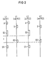
- the individual data records are transferred to the buffer memory PS already mentioned in the order in which they were created. This buffer memory is continuously checked for the presence of stored data records. If there is at least one such data record in the buffer memory, the data switching system EDS in turn transmits a request signal A (FIG. 2) via the dedicated lines L1 and L2 to the microprocessor arrangements PC1 and PC2 (FIG. 1) of the call data processing system under the control of the program control unit PE .
- a request signal is formed, for example, like the following also listed signals to be transmitted via the two dedicated lines, from a defined bit sequence.
- the two microprocessor arrangements PC1 and PC2 each emit a ready signal (B in FIG. 2) when they are ready to receive a data record, which may be present here for both.
- the data record to be transmitted next is copied in the data switching system EDS in the buffer memory PS and transmitted to the two microprocessor arrangements. (DS in FIG 2).
- the data record may contain security information, for example in the form of test marks, which permit such a check.
- Various methods for checking transmitted data signals based on backup information are already known, so that there is no need to go into them here. Examples of this are just security procedures using parity bits or block security procedures.
- the relevant data record is stored by them in the associated memory arrangement MP1 or PM2.
- Each of the two microprocessor arrangements then issues an acknowledgment signal (EQ1 in FIG. 2) to the data switching system via the associated dedicated line.
- the result of the aforementioned check of the received data record results from these acknowledgment signals.
- the data exchange system EDS concludes the transmission process by emitting a control signal ST1 (FIG. 2) to both microprocessor arrangements.
- This control signal indicates that the data record for further processing was received without errors in the two microprocessor arrangements.
- this control signal is emitted, the data record previously stored in the buffer memory PS of the data switching system is deleted.
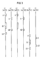
- FIG. 3 shows the case in which a data record transmitted by the data exchange system EDS could only be received without error by one of the microprocessor arrangements.
- This may be the microprocessor arrangement PC1, for example.
- This acknowledges receipt of the data record in the manner described above by issuing an acknowledgment signal EQ1 (positive acknowledgment signal).
- the microprocessor arrangement PC2 on the other hand, emits an acknowledgment signal EQ2, which indicates faulty reception (negative acknowledgment signal).
- the data switching system EDS now only outputs a control signal ST2 to the microprocessor arrangement from which the positive acknowledgment signal was previously received. In the present example, this is the microprocessor arrangement PC1.
- the control signal ST2 just mentioned tells the microprocessor arrangement PC1 that only the transmitted data record has been received without errors.
- the microprocessor arrangement PC1 now copies the data record previously received from it and stored in the memory arrangement MP1 and transmits this copied data record to the microprocessor arrangement PC2, which accepts this data record in the memory arrangement MP2.
- the aforementioned connection line L3 (FIG. 1) is used for this transmission, which takes place without the involvement of the data switching system EDS. Signals, for example, can be exchanged via this connection line between the two microprocessing arrangements for the signals explained above used for the delivery of a data record from the data switching system, as indicated in FIG. 3. After this transfer has been completed, the data record previously output by the data switching system is then available in the two memory arrangements MP1 and MP2 (FIG2) for further processing.
- the two microprocessor arrangements each have a floppy disk drive
- the data record to be transmitted is first transferred to a floppy disk by entering the aforementioned transmission command in the microprocessor arrangement PC1.
- the floppy disk contents can then be transferred to the memory array MP2 after the relevant diskettes have been inserted into the diskette drive of the microprocessor arrangement PC2.
- the counter arrangement Z shown in FIG. 1 can be used, for example, which may have two separate counter devices assigned to the microprocessor arrangements and controlled by a clock generator.
- these counting devices are each transferred from an initial state to a counting state in which they each count from an initial counter reading to a predetermined final counter reading. This final count determines the maximum time for the receipt of the acknowledgment signal.
Landscapes
- Engineering & Computer Science (AREA)
- Computer Networks & Wireless Communication (AREA)
- Signal Processing (AREA)
- Exchange Systems With Centralized Control (AREA)
- Data Exchanges In Wide-Area Networks (AREA)
- Telephonic Communication Services (AREA)
Applications Claiming Priority (2)
| Application Number | Priority Date | Filing Date | Title |
|---|---|---|---|
| DE3730106 | 1987-09-08 | ||
| DE3730106 | 1987-09-08 |
Publications (2)
| Publication Number | Publication Date |
|---|---|
| EP0306736A2 true EP0306736A2 (fr) | 1989-03-15 |
| EP0306736A3 EP0306736A3 (fr) | 1991-12-18 |
Family
ID=6335510
Family Applications (1)
| Application Number | Title | Priority Date | Filing Date |
|---|---|---|---|
| EP19880113282 Ceased EP0306736A3 (fr) | 1987-09-08 | 1988-08-16 | Procédé pour la transmission d'information de connexion mémorisée dans une installation de commutation de communications vers une installation de traitement d'information |
Country Status (3)
| Country | Link |
|---|---|
| US (1) | US5003460A (fr) |
| EP (1) | EP0306736A3 (fr) |
| ZA (1) | ZA886610B (fr) |
Cited By (2)
| Publication number | Priority date | Publication date | Assignee | Title |
|---|---|---|---|---|
| DE3912078A1 (de) * | 1989-04-13 | 1990-10-18 | Telefonbau & Normalzeit Gmbh | Digitale fernmeldevermittlungsanlage |
| DE4028997A1 (de) * | 1990-09-13 | 1992-03-19 | Telefonbau & Normalzeit Gmbh | Verfahren zur erfassung von verkehrsmessdaten in kommunikations-vermittlungsanlagen |
Families Citing this family (4)
| Publication number | Priority date | Publication date | Assignee | Title |
|---|---|---|---|---|
| US5742848A (en) * | 1993-11-16 | 1998-04-21 | Microsoft Corp. | System for passing messages between source object and target object utilizing generic code in source object to invoke any member function of target object by executing the same instructions |
| US7080060B2 (en) * | 2003-01-08 | 2006-07-18 | Sbc Properties, L.P. | System and method for intelligent data caching |
| US7827282B2 (en) * | 2003-01-08 | 2010-11-02 | At&T Intellectual Property I, L.P. | System and method for processing hardware or service usage data |
| US7660286B2 (en) * | 2006-02-03 | 2010-02-09 | Broadcom Corporation | Jitter management for packet data network backhaul of call data |
Family Cites Families (5)
| Publication number | Priority date | Publication date | Assignee | Title |
|---|---|---|---|---|
| IT1126475B (it) * | 1979-12-03 | 1986-05-21 | Honeywell Inf Systems | Apparato di comunicazione tra piu' processori |
| FR2477809B1 (fr) * | 1980-03-10 | 1987-08-21 | Jeumont Schneider | Systeme de transmission rapide de messages entre calculateurs |
| SE425282B (sv) * | 1981-01-30 | 1982-09-13 | Ericsson Telefon Ab L M | Datakommunikationsnet |
| DE3334773A1 (de) * | 1983-09-26 | 1984-11-08 | Siemens AG, 1000 Berlin und 8000 München | Verfahren zum betrieb eines in normalbetriebszeit parallel betriebenen speicherblockpaares |
| US4646300A (en) * | 1983-11-14 | 1987-02-24 | Tandem Computers Incorporated | Communications method |
-
1988
- 1988-08-16 EP EP19880113282 patent/EP0306736A3/fr not_active Ceased
- 1988-08-31 US US07/238,700 patent/US5003460A/en not_active Expired - Fee Related
- 1988-09-06 ZA ZA886610A patent/ZA886610B/xx unknown
Cited By (2)
| Publication number | Priority date | Publication date | Assignee | Title |
|---|---|---|---|---|
| DE3912078A1 (de) * | 1989-04-13 | 1990-10-18 | Telefonbau & Normalzeit Gmbh | Digitale fernmeldevermittlungsanlage |
| DE4028997A1 (de) * | 1990-09-13 | 1992-03-19 | Telefonbau & Normalzeit Gmbh | Verfahren zur erfassung von verkehrsmessdaten in kommunikations-vermittlungsanlagen |
Also Published As
| Publication number | Publication date |
|---|---|
| ZA886610B (en) | 1989-04-26 |
| EP0306736A3 (fr) | 1991-12-18 |
| US5003460A (en) | 1991-03-26 |
Similar Documents
| Publication | Publication Date | Title |
|---|---|---|
| DE3136128C2 (fr) | ||
| DE2350371C3 (de) | Verfahren und Einrichtung zur Prüfung und Wartung von Datenverarbeitungsanlagen mittels räumlich entfernter Wartungsstationen | |
| EP0658257B1 (fr) | Controleur de communication et procede de transmission d'informations | |
| DE102019130756A1 (de) | Steuerungseinheit-Diagnosevorrichtung und Verfahren davon | |
| DE4221841C2 (de) | Überwachungs-Kontrollsystem zur Überwachung mehrerer überwachter Geräte | |
| DE68908204T2 (de) | Nachrichtenverteilungssystem. | |
| EP0240833A1 (fr) | Dispositif de surveillance pour la surveillance du fonctionnement de dispositifs de transmission de la technique de transmission d'informations | |
| DE3639609A1 (de) | Einrichtung zur ueberpruefung von datenuebertragungsfehlern, insbesondere bei elektronischen registrierkassen | |
| EP0306736A2 (fr) | Procédé pour la transmission d'information de connexion mémorisée dans une installation de commutation de communications vers une installation de traitement d'information | |
| DE69015165T2 (de) | Einrichtung zur Bewertung der Übertragungsqualität. | |
| DE2903646B2 (de) | Schaltungsanordnung zum Ansteuern von Datenstationen in Datenübertragungsanlagen | |
| EP0106985B1 (fr) | Surveillance d'exploitation de voies de transmission numériques | |
| EP0182134B1 (fr) | Méthode de mise en oeuvre d'un système multicalculateurs à sécurité intrinsèque comportant plusieur circuits inprimés d'entrées/sorties à sécurité non intrinsèque | |
| DE69830231T2 (de) | Steuerverfahren für vermittlungseinheit und danach arbeitende anordnung | |
| DE3136586C2 (fr) | ||
| EP1221245B1 (fr) | Systeme, dispositif d'evaluation et procede de verification des donnees de communication relatives a une liaison, detectees par un central numerique | |
| DE3939631A1 (de) | Verfahren zur datenuebertragung und geraet zur datenuebertragung mit einem detektor zur erfassung einer falschen informationsverteilung | |
| DE3616556A1 (de) | Schaltungsanordnung zum ermitteln des synchronzustandes einer datenuebertragungsanlage | |
| DE69815335T2 (de) | Verfahren um Fehler auf einer seriellen Verbindung einer integrierten Schaltung zu erkennen und Vorrichtung zur Durchführung des Verfahrens | |
| DE3605359C2 (de) | Rechnersystem mit mehreren Rechnern | |
| EP0392245B1 (fr) | Adressage automatique d'unités de traitement d'un système numérique de transmission d'informations en assurant la surveillance et/ou la commande | |
| EP0214475A1 (fr) | Circuit pour transmettre des signaux de données entre des dispositifs de commande reliées entre eux par un système en anneaux | |
| EP0257314A2 (fr) | Méthode pour garantir l'opération d'un central de commutation commandé par programme | |
| DE19837216C2 (de) | Fehlerbehebung in einer Vermittlungseinrichtung eines Kommunikationssystems | |
| EP1680895A2 (fr) | Syst me de transmission de donn es dans un bus s riel bidirectionnel |
Legal Events
| Date | Code | Title | Description |
|---|---|---|---|
| PUAI | Public reference made under article 153(3) epc to a published international application that has entered the european phase |
Free format text: ORIGINAL CODE: 0009012 |
|
| AK | Designated contracting states |
Kind code of ref document: A2 Designated state(s): AT BE DE FR IT SE |
|
| 17P | Request for examination filed |
Effective date: 19901205 |
|
| PUAL | Search report despatched |
Free format text: ORIGINAL CODE: 0009013 |
|
| AK | Designated contracting states |
Kind code of ref document: A3 Designated state(s): AT BE DE FR IT SE |
|
| 17Q | First examination report despatched |
Effective date: 19930908 |
|
| RHK1 | Main classification (correction) |
Ipc: H04L 11/00 |
|
| STAA | Information on the status of an ep patent application or granted ep patent |
Free format text: STATUS: THE APPLICATION HAS BEEN REFUSED |
|
| 18R | Application refused |
Effective date: 19940227 |