EP0307068A2 - Circuit d'intégration à longue constante de temps - Google Patents
Circuit d'intégration à longue constante de temps Download PDFInfo
- Publication number
- EP0307068A2 EP0307068A2 EP88303438A EP88303438A EP0307068A2 EP 0307068 A2 EP0307068 A2 EP 0307068A2 EP 88303438 A EP88303438 A EP 88303438A EP 88303438 A EP88303438 A EP 88303438A EP 0307068 A2 EP0307068 A2 EP 0307068A2
- Authority
- EP
- European Patent Office
- Prior art keywords
- signal
- biphase
- circuit
- output port
- output
- Prior art date
- Legal status (The legal status is an assumption and is not a legal conclusion. Google has not performed a legal analysis and makes no representation as to the accuracy of the status listed.)
- Withdrawn
Links
Images

Classifications
-
- G—PHYSICS
- G06—COMPUTING OR CALCULATING; COUNTING
- G06G—ANALOGUE COMPUTERS
- G06G7/00—Devices in which the computing operation is performed by varying electric or magnetic quantities
- G06G7/12—Arrangements for performing computing operations, e.g. operational amplifiers specially adapted therefor
- G06G7/18—Arrangements for performing computing operations, e.g. operational amplifiers specially adapted therefor for integration or differentiation; for forming integrals
- G06G7/184—Arrangements for performing computing operations, e.g. operational amplifiers specially adapted therefor for integration or differentiation; for forming integrals using capacitive elements
- G06G7/186—Arrangements for performing computing operations, e.g. operational amplifiers specially adapted therefor for integration or differentiation; for forming integrals using capacitive elements using an operational amplifier comprising a capacitor or a resistor in the feedback loop
Definitions
- the invention relates generally to long time constant integration circuits providing an adjustable integration period utilizing capacitors of a size suitable for incorporation onto an integrated circuit with the integration circuit being capable of performing over a wide linear dynamic range with gain.
- a particularly useful circuit required in many communication applications is the integration circuit which performs the mathematical operation of integration.
- integration circuits There are many conventional integration circuits, three of which are illustrated in Figs. 1A, 1B and 1C. These circuits have been successfully used commercially. However, each of these only approximates the integration operation over a limited period of time.
- a basic integration circuit consists of a resistor R and a capacitor C and provides a limited version of the operation of mathematical integration. This is demonstrated by examining the output of the circuit in Figure 1A, to an input such as voltage step input.
- Formula 20, Figure 2 gives the value of the output voltage V out as a function of the time t, where t is the time base in seconds after the rising edge of the input step is applied, and as a function of the amplitude A of the step voltage applied to the input V in .
- FIG. 3 graphically shows the response of the circuit in Figure 1A.
- the step voltage applied to V in is represented by curve 30.
- Curve 31 represents V out (t) in circuit 1A and approximates the output of an ideal integrator, curve 32, when t is close to zero.
- Capacitor C must have a discharge voltage greater than V in to prevent a discharge.
- the period of integration must be less than the time capacitor C requires to reach a fully charged condition.
- Curve 33 which is a graphical representation of Formula 21, Figure 2 shows that the circuit 1A requires time to discharge. Therefore, the prior art circuit of Fig. 1A has limited applicability due to the limitations on capacitor size and period integration. Furthermore, during the discharge time represented by Curve 33, the circuit is useless for performing the integration function.
- the circuit of Fig. 1B also suffers, as the circuit of Fig. 1A, from requiring time to discharge in which the integration function cannot be performed. In order to decrease this discharge time, most integration circuits shunt a low resistance across the capacitor. It is not practical to reduce this resistor below a value of tens of ohms which still requires some recovery time.
- the circuit in Figure 1C illustrates a common base transistor circuit which functions as an integrator and provides a very close approximation of the ideal integrator.
- the bipolor junction transistor EBC shown in the circuit of Figure 1C is redrawn to the equivalent circuit using hybrid parameters and is shown in Figure 4.
- the emitter current is represented by i e .
- the collector current is shown as i c .
- the parameter h ie is equal to the short circuit input impedance.
- the parameter h oe is equal to the open circuit output admittance.
- the circuit is representable as a current source feeding a capacitor, as described by Formula 23, Figure 2, which is the mathematical representation of an ideal integrator.
- the circuit in Figure 1C is still vulnerable to the same problems of the circuits in Figs. 1A and 1B such as saturating and thus producing non-linearities.
- the circuit in Figure 1C must also be discharged before being usable again.
- the time constant of the common base integrator in Figure 1C is still directly proportional to the size of the capacitor C and thus is quite limited to those applications requiring only short time constants if the required capacitor is to be included in the integrated circuit.
- the circuit in Figure 1C cannot achieve variable integration time without using additional resistors, capacitors, switches and controls.
- Another object of the invention is to provide a voltage gain of the outputs when compared to alternative prior art designs.
- the invention comprises an apparatus that generates an integrated output signal that closely approximates the mathematical operation of integration for an input signal.
- a first means for modulating the input signal with a biphase signal.
- the biphase signal has an alternating positive and negative phase which changes at a rate corresponding to a repeating period of T seconds.
- the first means has an input port for receiving the input signal.
- An output port of the first means provides a modulated output signal corresponding to the input signal modulated with the biphase signal.
- a second means is provided for integrating the modulated output signal.
- the second means has an input port connected to the output port of the first means.
- An output port of the second means provides an integrated signal corresponding to the integrated, modulated output.
- the second means has a preferred period of time within which it operates. The preferred period is greater than T/2 seconds.
- a third means is provided for sampling the integrated signal every T/2 seconds and holding the sampled, integrated signal for T/2 seconds.
- the held, sampled signal corresponding to the negative biphase period is subtracted form the preceeding held, sampled signal corresponding to the positive biphase period.
- the third means has an input port connected to the output port of the second means and has an output port for providing a subtracted signal corresponding to the sampled, held, and subtracted integrated signals.
- a fourth means is provided for summing the subtracted signals.
- the fourth means has an input port connected to the output port of the third means.
- An output port of the fourth means provides the summed, subtracted signal whereby the summed, subtracted signal corresponds to the integrated input signal.
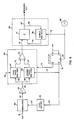
- FIG. 6 illustrates a block diagram of a circuit according to the invention.
- the square wave generator generator 88 provides a square wave signal adjusted to the desired amlitude required for modulator 60, adjusted to have a very narrow pulse width corresponding to the acquisition time of Sample and Hold (S/H) 78, and adjusted to a frequency that enables integrator 64 to remain operating in its linear range.
- Square wave generator 88 synchronizes modulator 60, first track and hold (T/H) 67, second T/H 69 via Flip/Flop 81 and S/H 78.
- the square wave signal is provided to FF 81 via line 82.
- FF 81 is configured so that during power up, Q will be initialized with zero and not-Q will be positive.
- the square wave signal at the Q port is provided via line 90 to level shifter 89 which changes the signal into alternating positive and negatives phases. This biphase timing signal is then provided to modulator 60 via line 62.
- Biphase modulator 60 receives the input signal f(t) via line 61.
- the biphase signal is a signal having a period T formed by alternating positive phase 103 and negative phase 104.
- the input and biphase signals are mixed (i.e. multiplied, combined, or modulated) and provided at the output port 63 of biphase modulator 60.
- Output port 63 of modulator 60 is connected to the input port of integrator 64 which integrates the modulated signal and provides the integrated, modulated signal at its output port 65.
- Integrator 64 is any conventional integration circuit having a linear operating range which is greater than T/2.
- the integrated output signal is provided via line 66 to track and hold circuit 67 and via line 68 to track and hold circuit 69.
- Each track and hold circuit is a standard off-the-shelf circuit well known in the prior art.
- the output of the circuit corresponds to the input of the circuit.
- the output of the circuit corresponds to the last tracked input immediately before the holding cycle began.
- First Track and hold (T/H) circuit 67 and second T/H circuit 69 are operated in synchronization with the biphase signal. This synchronization is provided by square wave generator 88.
- the signal provided via line 70 programs T/H 67 so that T/H is operated in its tracking cycle.
- the signal provided via line 70 programs T/H 67 to operate in its holding cycle.
- the signal provided via line 71 programs T/H 69 so that T/H 69 is operated in its holding cycle.
- the signal provided via line 71 programs T/H 69 to operate in its tracking cycle.
- FF 81 is clocked by a timing signal provided by square wave generator 88 via line 82. Positive 5 volts is applied to port J and K of FF 81. When J and K are both set high as shown, each clock pulse via line 82 wil toggle (reverse) both outputs Q and not-Q.
- the not-Q output of FF 81 is the inverse of the Q output of FF 81 which are fed to lines 70 and 71 respectively thus causing one T/H to be tracking while the other is holding.
- the held, integrated signal corresponding to the postive phase of the biphase modulation is provided by the output of first T/H 67 via line 72 to the sum port of a differential amplifier 74.
- the held, integrated signal corresponding to the negative phase of the the biphase modulation is provided by the output of the second T/H circuit 69 via line 73 to the difference port of the differential amplifier 74.
- the subtracted signal corresponding to the difference between the positive and its preceeding negative phase of the integrated signals is provided by the output of amplifier 74 via line 75 to one input port of a summing circuit such as summing amplifier 77.
- a feedback loop containing sample and hold (S/H) circuit 78 is connected across the summing amplifier 77.
- the output port 80 of the summing amplifier is connected via line 85 to the input port of the sample and hold circuit 78.
- the output port of the sample and hold circuit 78 is connected to the other input port of the summing amplifier 77 via line 76.
- the S/H 78 is synchronized with the biphase signal by the signal provided by square wave generator 88 via line 79 so that S/H 78 will sample at the end of each phase of the biphase signal and will hold throughout almost all of the next succeeding phase of the biphase signal.
- the sampling time must be extremely short when compared to the period of the biphase modulation so the held signal closely approximates the last value in line 85 at the moment before the phase changes.
- the acquisition time of S/H 78 is very short, i.e. nanoseconds, no positive feedback as a consequence of S/H 78 being connected across summing amplifier 77 will occur during the brief sampling period.
- S/H that will meet this requirement.
- feedback during the sampling period can also be prevented by installing a delay either on line 76 or on line 85.
- the summing amplifier 77 outputs the integrated input signal f(t) corresponding to the summed, subtracted signal via line 80.
- the alternative embodiment of an integration circuit 64 as shown in Figure 7 would replace the integrator 64 in Figure 6.
- the modulated signal 63 is connected to a differential amplifier 700 such as disclosed in U.S. Patent No. 4,511,852.
- a modulated signal corresponding to the modulated signal 63 is provided at output port 701 and is connected to a first integrator 703.
- An inverse of the modulated signal 63 is provided at output port 702 and is connected to a second integrator 704.
- An integrated signal corresponding to the integrated, modulated signal is provided at output port 705 is connected to the sum port of the differential amplifier 707.
- the inverse integrated signal at the output port 706 is the inverse of the integrated signal at output port 705.
- the inverse integrated signal corresponds to the inverse of the integrated, modulated input signal and is connected to the differential port of the differential amplifier 707.
- Differential amplifier 707 subtracts the integrated signal from the inverse integrated signal resulting in an integrated signal free from offset bias and twice the amplitude of the first integrated signal. If twice the value of the integrated signal is not required, then a voltage divider or similar means may be inserted in line 65 to return the integrated signal to the non-amplified value.
- the integrated signal is connected via line 65 to the third means 83 for partitioning the integrated signal into intervals.
- the preferred embodiment of the third means 83 for partitioning the integrated signal into intervals is shown using track and hold circuits.
- sample and hold circuits could be used instead of each track and hold without altering the performance of the invention. If sample and hold circuits are substituted, then the apparatus for cycling the sample and hold circuits, corresponding to FF 81 in the case of the preferred embodiment of using track and hold circuits, would have to be modified corresponding to the characteristics of the sample and hold circuits selected.
- Each sample and hold circuit is a standard off-the-shelf circuit well known in the prior art.
- the preferred embodiment of the fourth means 84 is shown using a sample and hold circuit 78 in combination with a summing circuit 77.
- a track and hold circuit cannot be substituted for the sample and hold circuit 78.
- Each of these circuits is also standard off-the-shelf circuits well known in the prior art.
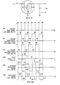
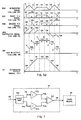
- Figures 5A and 5B illustrate a timing diagram of the various signals which would be generated by the invention as illustrated in block diagram form in Figure 6.
- Graph 503 in Figure 5A illustrates the input signal which may be applied via line 61 to biphase modulator 60.
- the input signal is assumed to be a step function of amplitude A comprising a positive step 100 followed by no signal 101 followed by a negative step 102 with a period of T.
- Graph 500 illustrates the square wave signal provided by square wave generator 88 via lines 82 and 79. Pulses 146-153 occur every T/2 seconds with T/2 being much greater than the width of the pulses.
- Graph 501 illustrates the output of FF 81 that is provided to level shifter 89 via line 90.
- the output is a series of positive steps 154, 156, 158, and 160 followed by zero steps, 155, 157 and 159 respectively.
- the width of each pulse is T/2 seconds.
- Graph 504 illustrates the biphase signal with a period T provided by the level shifter via line 62 corresponding to the square wave signal with a 50 percent duty cycle provided by FF 81 via line 90.
- Graph 504 illustrates the biphase signal which is provided via line 62 for mixing with the input signal illustrated in Graph 503.
- the biphase signal is a series of alternating positive steps 103 and negative steps 104.
- the biphase signal is mixed (i.e. modulated) with the input signal to provide a modulated output signal via line 63.
- Graph 505 illustrates the modulated output signal that is provided to the integrator 64 via line 63.
- the period T of the biphase signal provided via line 62 and as illustrated in graph 504 is selected such that T/2 enables the integrator 64 to be operated continously without exceeding its linear operating range.
- positive steps 105, 107 and negative step 106 result from mixing the positive input step 100 with the alternating positive steps 103 and negative steps 104 of the modulating signal. Between steps 107 and 108, no signal 101 is provided and corresponds to no signal 101 in graph 503. Negative step 102 now corresponds to negative steps 108, 110 and positive step 110.
- Graph 506 in Figure 5B illustrates the continuous operation of integrator 64 and its corresponding output provided via line 65.
- the signal corresponding to the integral of positive step 105 is positive slope 111.
- the signal corresponding to the integral of negative step 106 is negative slope 112.
- positive slope 113 corresponding to the integral of positive step 107.
- Zero slope 114 corresponds to the integral of no signal 101.
- Negative slope 115 corresponds to the integral of negative step 108.
- Positive slope 116 corresponds to the integral of positive step 109.
- Negative slope 117 corresponds to the integral of negative step 110.
- integrator 64 will operate continuously and linearly as shown without needing periodic charge dumping and resetting.
- the maximum absolute value of the amplitude of any integrated intervals resulting from the positive and negative phases of the modulating signal illustrated by slopes 111 through 117 in graph 506 must be less than the amplitude required to cause integrator 64 to be driven into a non-linear operating range.
- Graphs 507 illustrates the partitioning of the integrated signal via line 65 into a first T/H signal provided via line 72 corresponding to the intervals of integration occurring during positive phases of the biphase signal and into a second T/H signal provided via line 73 corresponding to the intervals of integration occurring during negative phases of the biphase signal.
- Each interval of Graph 507 labeled T correspond to a positive phase of the biphase signal.
- Each interval of Graph 507 marked H corresponds to a negative phase of the biphase signal.
- the intervals marked T correspond to T/H 67's tracking periods for T/2 seconds.
- the intervals marked H correspond to T/H 67's holding periods for T/2 seconds.
- the timing signal which is the square wave signal illustrated by Graph 502 in Figure 5A and provided by line 70 causes T/H to alternatingly track then hold every T/2 seconds.
- Zero steps 160, 163, and 165 illustrated in Graph 502 provide tracking intervals 118, 120, and 122 illustrated in Graph 507 in Figure 5B.
- positive steps 162, 164, and 166 illustrated in Graph 502 in Figure 5A cause T/H 67 to hold which is illustrated by holding intervals 119, 121, and 123 in Graph 507 in Figure 5B.
- the tracking periods in Graph 507 are positive slope 118 which corresponds to positive slope 111; positive and level slope 120 corresponds to postive slope 113; level and negative slope 122 corresponds to positive slope 115, and negative slope 124 corresponds to negative slope 117.
- Zero slopes 119, 121, 123 correspond to the holding period of T/2 seconds which immediately follows the tracking period of T/2 seconds.
- Graph 507 illustrates by zero slopes 119, 121, and 123 that the amplitude immediately tracked at the ending of the first T/2 seconds is held for T/2 seconds.
- Graph 508 illustrates the partitioning of the integrated signal provided via line 65 into second T/H signal corresponding to the output of T/H 69 provided at line 73.
- Each interval of Graph 508 marked T corresponds to a negative phase of the biphase signal.
- Each interval of Graph 508 marked H corresponds to a positive phase of the biphase signal.
- the intervals marked T correspond to T/H 69's tracking periods for T/2 seconds.
- the intervals marked H correspond to T/H 69's holding periods for T/2 seconds.
- the square wave signal illustrated by Graph 501 in Figure 5A and provided by line 71 causes T/H to alternatingly track then hold every T/2 seconds.
- Zero steps 155, 157, and 159 illustrated in Graph 501 in Figure 5A provide tracking intervals 126, 128, and 130 illustrated in Graph 508 in Figure 5B.
- positive steps 155, 156, and 158 illustrated in Graph 501 in Figure 5A cause T/H 69 to hold which is illustrated by holding intervals 125, 127, and 129 in Graph 508 in Figure 5B.
- the tracking periods in Graph 508 are negative slope 126 which corresponds to negative slope 112, zero slope 128 corresponds to zero slope 114, and positive slope 130 corresponds to positive slope 116.
- Zero slopes 127, 129, and 131 correspond to the holding period of T/2 seconds which immediately follows the tracking period of T/2 seconds. Again, as in Graph 507, the amplitude that is tracked immediately at the end of the first T/2 seconds is held for the next T/2 seconds.
- Graph 508 illustrates the signal that is provided by line 73.
- Graph 509 illustrates the subtracted signal provided via line 75 that is provided at the output of differential amplifier 74.
- Positive slope 132 corresponds to the signal obtained when zero slope 125 is subtracted from positive slope 118.
- Positive slope 133 corresponds to the signal obtained when negative slope 126 is subtracted form zero slope 119.
- Positive slope 134 corresponds to the signal obtained when zero slope 127 is subtracted from positive slope 120.
- Zero slope 135 corresponds to the signal obtained when zero slope 128 is subtracted from zero slope 121.
- Negative slope 136 corresponds to the signal obtained when zero slope 129 is subtracted from negative slope 122.
- Negative slope 136 corresponds to the signal obtained when positve slope 130 is subtracted from zero slope 123.
- Negative slope 138 corresponds to the signal obtained when zero slope 131 is subtracted from negative slope 124.
- Graph 511 illustrates the integrated output signal corresponding to the integral of f(t).
- the signal provided at the output of the differential amplifier 74 is combined using the summing amplifier 77 and S/H 78.
- S/H 78 is timed via line 79 and as shown in Graph 500 in Figure 5A to sample the signal at the end of the first T/2 seconds and hold that value for T/2 seconds.
- pulse 146 shown in Graph 500 causes the signal provided by line 85 to be held which corresponds to zero slope 167 in Graph 510 in Figure 5B.
- Pulse 147 causes the S/H 78 to hold zero slope 168.
- pulse 148 corresponds to zero slope 169
- pulse 149 corresponds to zero slope 170
- pulse 150 corresponds to zero slope 171
- pulse 151 corresponds to zero slope 172
- pulse 152 corresponds to zero slope 173.
- the sample period caused by the pulses 146-152 in Graph 500 in Figure 5A represent a very short time interval. Therefore, the value present in summing amplifier 77 provided by line 85 at the time of phase shift of the biphase signal is held, designated as H in Graph 510 in Figure 5B, until the next succeeding phase shift of the biphase signal.
- interval 139 is obtained by adding zero slope 167 to the positive slope 132 in summing amplifier 77.
- Interval 140 is obtained by adding the value sampled at the end of T/2 seconds from positive slope 139 which corresponds to zero slope 168 to positive slope 1323.
- Interval 141 is obtained by adding the value sampled at the end of T/2 seconds from interval 140 which corresponds to zero slope 169 to positive slope 134.
- Interval 142 is obtained by adding the value sampled at the end of T/2 seconds from interval 141 which corresponds to 170 to zero slope 135.
- Interval 143 is obtained by adding the value sampled at the end of T/2 seconds from interval 142 which corresponds to zero slope 171 to negative slope 136.
- Interval 144 is obtained by adding the value sampled at the end of T/2 seconds from interval 143 which corresponds to zero slope 172 to negative slope 137.
- Interval 145 is obtained by adding the value sampled at the end of T/2 seconds from interval 144 which corresponds to zero slope 173 to negative slope 138.
Landscapes
- Engineering & Computer Science (AREA)
- Physics & Mathematics (AREA)
- Mathematical Physics (AREA)
- Theoretical Computer Science (AREA)
- Power Engineering (AREA)
- Software Systems (AREA)
- Computer Hardware Design (AREA)
- General Physics & Mathematics (AREA)
- Manipulation Of Pulses (AREA)
- Stabilization Of Oscillater, Synchronisation, Frequency Synthesizers (AREA)
- Radar Systems Or Details Thereof (AREA)
- Analogue/Digital Conversion (AREA)
Applications Claiming Priority (2)
| Application Number | Priority Date | Filing Date | Title |
|---|---|---|---|
| US07/082,712 US4814714A (en) | 1987-08-07 | 1987-08-07 | Long time constant integrating circuit |
| US82712 | 2002-02-25 |
Publications (2)
| Publication Number | Publication Date |
|---|---|
| EP0307068A2 true EP0307068A2 (fr) | 1989-03-15 |
| EP0307068A3 EP0307068A3 (fr) | 1990-01-24 |
Family
ID=22172950
Family Applications (1)
| Application Number | Title | Priority Date | Filing Date |
|---|---|---|---|
| EP88303438A Withdrawn EP0307068A3 (fr) | 1987-08-07 | 1988-04-15 | Circuit d'intégration à longue constante de temps |
Country Status (5)
| Country | Link |
|---|---|
| US (1) | US4814714A (fr) |
| EP (1) | EP0307068A3 (fr) |
| JP (1) | JPS6451590A (fr) |
| CA (1) | CA1287176C (fr) |
| GB (1) | GB2208555B (fr) |
Families Citing this family (10)
| Publication number | Priority date | Publication date | Assignee | Title |
|---|---|---|---|---|
| US5043608A (en) * | 1989-08-24 | 1991-08-27 | Tektronix, Inc. | Avalanche photodiode non-linearity cancellation |
| US5304939A (en) * | 1991-06-28 | 1994-04-19 | Digital Equipment Corporation | Tracking peak detector |
| EP0522578A3 (en) * | 1991-07-12 | 1993-06-16 | Pioneer Electronic Corporation | Noise removing circuit |
| US5225776A (en) * | 1991-10-07 | 1993-07-06 | Tektronix, Inc. | Method and apparatus for probing and sampling an electrical signal |
| DE69304460T2 (de) * | 1992-06-29 | 1997-03-13 | Murata Manufacturing Co | Driftunterdrückungsschaltung für Gyrometer |
| DE69521245T2 (de) * | 1994-08-08 | 2001-09-20 | Sharp K.K., Osaka | Abtast- und Halterschaltung |
| JP2561040B2 (ja) * | 1994-11-28 | 1996-12-04 | 日本電気株式会社 | 容量型センサの容量変化検出回路およびその検出方法 |
| US5585756A (en) * | 1995-02-27 | 1996-12-17 | University Of Chicago | Gated integrator with signal baseline subtraction |
| US6536302B1 (en) | 1999-03-24 | 2003-03-25 | Magna Seating Systems Inc. | Manual adjustment mechanism for a vehicle |
| US7701256B2 (en) * | 2006-09-29 | 2010-04-20 | Analog Devices, Inc. | Signal conditioning circuit, a comparator including such a conditioning circuit and a successive approximation converter including such a circuit |
Family Cites Families (8)
| Publication number | Priority date | Publication date | Assignee | Title |
|---|---|---|---|---|
| US3927378A (en) * | 1970-11-23 | 1975-12-16 | Ericsson Telefon Ab L M | Demodulator |
| US3731208A (en) * | 1971-05-17 | 1973-05-01 | Storage Technology Corp | Apparatus for and method of integration detection |
| GB1347776A (en) * | 1971-10-29 | 1974-02-27 | Integrated Photomatrix Ltd | Pulse charge to voltage converter |
| US3740586A (en) * | 1971-12-13 | 1973-06-19 | Electro Dev Corp | Pulse width - dc converter compensating for pulse repetition rate changes |
| US3879724A (en) * | 1973-11-19 | 1975-04-22 | Vidar Corp | Integrating analog to digital converter |
| US4160922A (en) * | 1977-08-02 | 1979-07-10 | Exxon Production Research Company | Method of generating a direct current control signal from a noisy alternating current signal |
| US4390844A (en) * | 1980-12-24 | 1983-06-28 | California Institute Of Technology | Integration filter for step waveforms |
| US4511852A (en) * | 1983-01-31 | 1985-04-16 | Hazeltine Corporation | Differential amplifier having balanced output |
-
1987
- 1987-08-07 US US07/082,712 patent/US4814714A/en not_active Expired - Fee Related
-
1988
- 1988-04-06 CA CA000563420A patent/CA1287176C/fr not_active Expired - Fee Related
- 1988-04-15 EP EP88303438A patent/EP0307068A3/fr not_active Withdrawn
- 1988-04-15 GB GB8809001A patent/GB2208555B/en not_active Expired - Fee Related
- 1988-05-20 JP JP63123762A patent/JPS6451590A/ja active Pending
Also Published As
| Publication number | Publication date |
|---|---|
| GB2208555A (en) | 1989-04-05 |
| GB8809001D0 (en) | 1988-05-18 |
| JPS6451590A (en) | 1989-02-27 |
| EP0307068A3 (fr) | 1990-01-24 |
| GB2208555B (en) | 1992-01-08 |
| CA1287176C (fr) | 1991-07-30 |
| US4814714A (en) | 1989-03-21 |
Similar Documents
| Publication | Publication Date | Title |
|---|---|---|
| US5150324A (en) | Analog arithmetic circuit that can perform multiplication division expansion and compression by using delta sigma modulator | |
| US4843339A (en) | Isolation amplifier including precision voltage-to-duty-cycle converter and low ripple, high bandwidth charge balance demodulator | |
| CA1246253A (fr) | Generateur de salves de signaux modules par deplacement de frequence ou modules en frequence | |
| US6577691B2 (en) | Precision timing generator apparatus and associated methods | |
| US6304623B1 (en) | Precision timing generator system and method | |
| US6795001B2 (en) | Analog FIR-filter with Σ Δ modulator and delay line | |
| US4342119A (en) | Multi-tone jammer | |
| DE3101589C2 (de) | Frequenzsyntheseanordnung | |
| US4814714A (en) | Long time constant integrating circuit | |
| US6346852B1 (en) | Class-D amplifier with enhanced bandwidth | |
| CA2342417A1 (fr) | Compensation adaptative de phase de signal porteur | |
| Gray et al. | A precision sample and hold circuit with subnanosecond switching | |
| US4425515A (en) | Method and means to minimize risetime of a microwave pulse modulated signal from a frequency multiplier circuit | |
| JPS58112979U (ja) | 送信機によつて発生された搬送波と側帯波との位相を制御する装置 | |
| US4439689A (en) | Circuit for the control of the cyclic ratio of a periodic pulse signal and device multiplying by 2n of a pulse signal frequency incorporating said control circuit | |
| US4468636A (en) | Low temperature coefficient wide band-width voltage controlled oscillator | |
| US3783304A (en) | Constant pulse width generator | |
| US4361769A (en) | Method for performing a sample and hold function | |
| US4247823A (en) | Low noise, low phase shift analog signal multiplier | |
| GB2247123A (en) | Analog to duty-cycle modulation | |
| US4706047A (en) | Frequency extended digitally generated FM | |
| JPH05266687A (ja) | ダイナミックバイアス回路 | |
| Bohme et al. | The chaotizer-dechaotizer-channel | |
| US6225864B1 (en) | RF amplifier having a dual slope phase modulator | |
| SU1665530A1 (ru) | Частотный модул тор |
Legal Events
| Date | Code | Title | Description |
|---|---|---|---|
| PUAI | Public reference made under article 153(3) epc to a published international application that has entered the european phase |
Free format text: ORIGINAL CODE: 0009012 |
|
| AK | Designated contracting states |
Kind code of ref document: A2 Designated state(s): DE IT |
|
| PUAL | Search report despatched |
Free format text: ORIGINAL CODE: 0009013 |
|
| AK | Designated contracting states |
Kind code of ref document: A3 Designated state(s): DE IT |
|
| 17P | Request for examination filed |
Effective date: 19900703 |
|
| 17Q | First examination report despatched |
Effective date: 19930118 |
|
| STAA | Information on the status of an ep patent application or granted ep patent |
Free format text: STATUS: THE APPLICATION HAS BEEN WITHDRAWN |
|
| 18W | Application withdrawn |
Withdrawal date: 19930909 |