EP0307597A1 - Gedruckte Schaltungsmutterkarte für Mikroprozessorbusse - Google Patents
Gedruckte Schaltungsmutterkarte für Mikroprozessorbusse Download PDFInfo
- Publication number
- EP0307597A1 EP0307597A1 EP88112310A EP88112310A EP0307597A1 EP 0307597 A1 EP0307597 A1 EP 0307597A1 EP 88112310 A EP88112310 A EP 88112310A EP 88112310 A EP88112310 A EP 88112310A EP 0307597 A1 EP0307597 A1 EP 0307597A1
- Authority
- EP
- European Patent Office
- Prior art keywords
- mother board
- printed circuit
- ground
- tracks
- microprocessors
- Prior art date
- Legal status (The legal status is an assumption and is not a legal conclusion. Google has not performed a legal analysis and makes no representation as to the accuracy of the status listed.)
- Withdrawn
Links
- 238000003466 welding Methods 0.000 claims abstract description 4
- 239000002184 metal Substances 0.000 description 3
- 239000011810 insulating material Substances 0.000 description 1
- 238000000034 method Methods 0.000 description 1
Images

Classifications
-
- H—ELECTRICITY
- H05—ELECTRIC TECHNIQUES NOT OTHERWISE PROVIDED FOR
- H05K—PRINTED CIRCUITS; CASINGS OR CONSTRUCTIONAL DETAILS OF ELECTRIC APPARATUS; MANUFACTURE OF ASSEMBLAGES OF ELECTRICAL COMPONENTS
- H05K1/00—Printed circuits
- H05K1/02—Details
- H05K1/0213—Electrical arrangements not otherwise provided for
- H05K1/0216—Reduction of cross-talk, noise or electromagnetic interference
- H05K1/0218—Reduction of cross-talk, noise or electromagnetic interference by printed shielding conductors, ground planes or power plane
- H05K1/0219—Printed shielding conductors for shielding around or between signal conductors, e.g. coplanar or coaxial printed shielding conductors
-
- H—ELECTRICITY
- H05—ELECTRIC TECHNIQUES NOT OTHERWISE PROVIDED FOR
- H05K—PRINTED CIRCUITS; CASINGS OR CONSTRUCTIONAL DETAILS OF ELECTRIC APPARATUS; MANUFACTURE OF ASSEMBLAGES OF ELECTRICAL COMPONENTS
- H05K2201/00—Indexing scheme relating to printed circuits covered by H05K1/00
- H05K2201/04—Assemblies of printed circuits
- H05K2201/044—Details of backplane or midplane for mounting orthogonal PCBs
-
- H—ELECTRICITY
- H05—ELECTRIC TECHNIQUES NOT OTHERWISE PROVIDED FOR
- H05K—PRINTED CIRCUITS; CASINGS OR CONSTRUCTIONAL DETAILS OF ELECTRIC APPARATUS; MANUFACTURE OF ASSEMBLAGES OF ELECTRICAL COMPONENTS
- H05K2201/00—Indexing scheme relating to printed circuits covered by H05K1/00
- H05K2201/09—Shape and layout
- H05K2201/09209—Shape and layout details of conductors
- H05K2201/09218—Conductive traces
- H05K2201/09236—Parallel layout
-
- H—ELECTRICITY
- H05—ELECTRIC TECHNIQUES NOT OTHERWISE PROVIDED FOR
- H05K—PRINTED CIRCUITS; CASINGS OR CONSTRUCTIONAL DETAILS OF ELECTRIC APPARATUS; MANUFACTURE OF ASSEMBLAGES OF ELECTRICAL COMPONENTS
- H05K2201/00—Indexing scheme relating to printed circuits covered by H05K1/00
- H05K2201/09—Shape and layout
- H05K2201/09209—Shape and layout details of conductors
- H05K2201/09654—Shape and layout details of conductors covering at least two types of conductors provided for in H05K2201/09218 - H05K2201/095
- H05K2201/09727—Varying width along a single conductor; Conductors or pads having different widths
-
- H—ELECTRICITY
- H05—ELECTRIC TECHNIQUES NOT OTHERWISE PROVIDED FOR
- H05K—PRINTED CIRCUITS; CASINGS OR CONSTRUCTIONAL DETAILS OF ELECTRIC APPARATUS; MANUFACTURE OF ASSEMBLAGES OF ELECTRICAL COMPONENTS
- H05K3/00—Apparatus or processes for manufacturing printed circuits
- H05K3/40—Forming printed elements for providing electric connections to or between printed circuits
- H05K3/42—Plated through-holes or plated via connections
Definitions
- the present invention generally relates to the field of printed circuit boards and, more particularly, to a mother board provided with printed circuit, for busses of microprocessors of improved type as far as the electrical ground is concerned.
- the conventional printed circuit cards or boards for use in microprocessors are generally formed of a plate of insulating material on both surfaces of which the electrically conductive metal tracks forming the circuits intended to connect the several board components and to connect the board to the microprocessor are printed.
- Such boards are provided with an electrical ground layer generally located intermediate the two surfaces on which the electrically conductive metal tracks are printed.
- the mother boards will exhibit a treshold to the clock frequency to which they can operate and beyond this treshold the signals flowing in these tracks of the printed circuit can interfere therebetween.
- the object of the present invention is to provide a printed circuit mother board improved as far as the electrical ground is concerned so as to permit this mother board to be able to operate at high clock frequency without any interference among the signals flowing in adjacent tracks of the printed circuit.
- the printed circuit mother board for busses of microprocessors is characterized in that each track of the printed circuit is separated from the adjacent one by a ground track which permits the signals flowing in said printed circuit tracks to be insulated from each other and this both on the component side and the welding side of the mother board.
- ground tracks provided on one surface of the printed circuit mother board are electrically connected to the ground tracks provided on the opposite surface of the printed circuit mother board.
- the ground tracks on both the surfaces of the mother board are connected to each other by ground bridges.
- the ground tracks lie all on the same plane.
- numeral 1 designates the printed circuit mother board according to the present invention, which is suitable for busses of microprocessors.
- the metal circuit tracks 4 are printed. Between each of the printed circuit tracks 4 and the adjacent one a ground track 5 is provided.
- ground tracks applied on both the surfaces 2 and 3 of the mother board 1 are electrically connected to each other by means of connecting bridges 6, so that all the ground tracks 5 are practically in contact to each other.
- the mother board can operate with high clock frequency without causing any interference among the signals flowing in the several tracks, thereby making the mother board very effective.
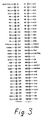
- a lower number of possibility given by the microprocessor has been used, thereby limiting the conventional connector to the external bus to 64 pins only (32 for each surface), but obtaining as a reward a high noise-immunity with a two face printed circuit instead of a multilayer printed circuit.
- FIG. 3 A layout of the arrangement of pins of this connector to the external bus is shown in Fig. 3.
- CLK and EXDTACK signals are further protected because the adjacent pins C32 and C1 respectively are also in ground connection.
- the width and the thickness of the ground tracks are not critical for the present invention.
- the ground tracks can be applied by means of any known method and means.
- the mother board according to the present invention permitting to operate with high clock frequency provides such performances that the mother boards with printed circuits on both the surfaces at present available on the market cannot provide.
Landscapes
- Physics & Mathematics (AREA)
- Electromagnetism (AREA)
- Engineering & Computer Science (AREA)
- Microelectronics & Electronic Packaging (AREA)
- Combinations Of Printed Boards (AREA)
- Structure Of Printed Boards (AREA)
Applications Claiming Priority (2)
| Application Number | Priority Date | Filing Date | Title |
|---|---|---|---|
| IT2233087U IT211826Z2 (it) | 1987-09-15 | 1987-09-15 | Scheda madre a circuito stampato per bus di microprocessori. |
| IT2233087U | 1987-09-15 |
Publications (1)
| Publication Number | Publication Date |
|---|---|
| EP0307597A1 true EP0307597A1 (de) | 1989-03-22 |
Family
ID=11194761
Family Applications (1)
| Application Number | Title | Priority Date | Filing Date |
|---|---|---|---|
| EP88112310A Withdrawn EP0307597A1 (de) | 1987-09-15 | 1988-07-29 | Gedruckte Schaltungsmutterkarte für Mikroprozessorbusse |
Country Status (2)
| Country | Link |
|---|---|
| EP (1) | EP0307597A1 (de) |
| IT (1) | IT211826Z2 (de) |
Cited By (6)
| Publication number | Priority date | Publication date | Assignee | Title |
|---|---|---|---|---|
| DE3922238A1 (de) * | 1989-07-06 | 1991-01-10 | Telefonbau & Normalzeit Gmbh | Ausfuehrung und anordnung von elektronischen baugruppen |
| EP0371696A3 (de) * | 1988-11-30 | 1991-07-24 | Hitachi, Ltd. | Elektronisches System mit einem Mikroprozessor und Koprozessor, die auf einer Schaltplatte montiert sind |
| EP0389976A3 (de) * | 1989-03-27 | 1992-08-26 | Matsushita Electric Industrial Co., Ltd. | Vorrichtung für eine Leistungs-Hochspannungsquelle |
| EP1037512A3 (de) * | 1999-03-18 | 2002-06-19 | Molex Incorporated | Flexibles Flachkabel mit Erdleitern |
| EP1029431A4 (de) * | 1997-10-28 | 2002-07-24 | Intel Corp | Verbindungslochkonfigurationzurunterstützung einer gleichmässigen übertragungsleitungsstruktur |
| GB2429145A (en) * | 2005-08-20 | 2007-02-21 | Bart Milner | A food tray container |
Citations (1)
| Publication number | Priority date | Publication date | Assignee | Title |
|---|---|---|---|---|
| US4130723A (en) * | 1976-11-19 | 1978-12-19 | The Solartron Electronic Group Limited | Printed circuit with laterally displaced ground and signal conductor tracks |
-
1987
- 1987-09-15 IT IT2233087U patent/IT211826Z2/it active
-
1988
- 1988-07-29 EP EP88112310A patent/EP0307597A1/de not_active Withdrawn
Patent Citations (1)
| Publication number | Priority date | Publication date | Assignee | Title |
|---|---|---|---|---|
| US4130723A (en) * | 1976-11-19 | 1978-12-19 | The Solartron Electronic Group Limited | Printed circuit with laterally displaced ground and signal conductor tracks |
Cited By (6)
| Publication number | Priority date | Publication date | Assignee | Title |
|---|---|---|---|---|
| EP0371696A3 (de) * | 1988-11-30 | 1991-07-24 | Hitachi, Ltd. | Elektronisches System mit einem Mikroprozessor und Koprozessor, die auf einer Schaltplatte montiert sind |
| EP0389976A3 (de) * | 1989-03-27 | 1992-08-26 | Matsushita Electric Industrial Co., Ltd. | Vorrichtung für eine Leistungs-Hochspannungsquelle |
| DE3922238A1 (de) * | 1989-07-06 | 1991-01-10 | Telefonbau & Normalzeit Gmbh | Ausfuehrung und anordnung von elektronischen baugruppen |
| EP1029431A4 (de) * | 1997-10-28 | 2002-07-24 | Intel Corp | Verbindungslochkonfigurationzurunterstützung einer gleichmässigen übertragungsleitungsstruktur |
| EP1037512A3 (de) * | 1999-03-18 | 2002-06-19 | Molex Incorporated | Flexibles Flachkabel mit Erdleitern |
| GB2429145A (en) * | 2005-08-20 | 2007-02-21 | Bart Milner | A food tray container |
Also Published As
| Publication number | Publication date |
|---|---|
| IT8722330V0 (it) | 1987-09-15 |
| IT211826Z2 (it) | 1989-05-25 |
Similar Documents
| Publication | Publication Date | Title |
|---|---|---|
| US4434321A (en) | Multilayer printed circuit boards | |
| US3491267A (en) | Printed circuit board with elevated bus bars | |
| JP3330387B2 (ja) | 可撓性多層回路配線基板 | |
| EP0039175A2 (de) | Elektrische Steckeranordnung für Leiterplatten | |
| JPS6298580A (ja) | プロ−ブ・ケ−ブル | |
| US6661674B2 (en) | System comprising at least two printed circuit boards | |
| GB1269592A (en) | Sub-element for electronic circuit board | |
| EP0307597A1 (de) | Gedruckte Schaltungsmutterkarte für Mikroprozessorbusse | |
| JPH05102621A (ja) | 導電パターン | |
| JPH0715106A (ja) | プリント基板 | |
| JPS61127195A (ja) | プリント配線基板接続体 | |
| JPH02144991A (ja) | 親子基板の実装方法 | |
| JPH0710514Y2 (ja) | フレキシブルプリント配線板 | |
| JPS6141272Y2 (de) | ||
| JPS60140782A (ja) | チツプ部品実装プリント基板 | |
| JPS5818992A (ja) | 回路部材の接続構造 | |
| JPS58202584A (ja) | 電子部品の実装構造 | |
| JPH0255957B2 (de) | ||
| JPH08779Y2 (ja) | 多層プリント板 | |
| JPS6024088A (ja) | 試験用プリント基板の製造方法 | |
| JPH05144492A (ja) | プリント基板の実装方法 | |
| JPH08316595A (ja) | フレキシブル回路板 | |
| JPS62155587A (ja) | 配線基板 | |
| JPS60143510A (ja) | 給配電母線 | |
| JPH0634432B2 (ja) | 配線回路基板 |
Legal Events
| Date | Code | Title | Description |
|---|---|---|---|
| PUAI | Public reference made under article 153(3) epc to a published international application that has entered the european phase |
Free format text: ORIGINAL CODE: 0009012 |
|
| AK | Designated contracting states |
Kind code of ref document: A1 Designated state(s): AT BE CH DE ES FR GB GR LI LU NL SE |
|
| STAA | Information on the status of an ep patent application or granted ep patent |
Free format text: STATUS: THE APPLICATION IS DEEMED TO BE WITHDRAWN |
|
| 18D | Application deemed to be withdrawn |
Effective date: 19890923 |