EP0308152A2 - Circuit intégré MIS ainsi que son procédé de fabrication - Google Patents
Circuit intégré MIS ainsi que son procédé de fabrication Download PDFInfo
- Publication number
- EP0308152A2 EP0308152A2 EP88308388A EP88308388A EP0308152A2 EP 0308152 A2 EP0308152 A2 EP 0308152A2 EP 88308388 A EP88308388 A EP 88308388A EP 88308388 A EP88308388 A EP 88308388A EP 0308152 A2 EP0308152 A2 EP 0308152A2
- Authority
- EP
- European Patent Office
- Prior art keywords
- type
- regions
- semiconductor
- region
- impurity
- Prior art date
- Legal status (The legal status is an assumption and is not a legal conclusion. Google has not performed a legal analysis and makes no representation as to the accuracy of the status listed.)
- Withdrawn
Links
Images

Classifications
-
- H—ELECTRICITY
- H10—SEMICONDUCTOR DEVICES; ELECTRIC SOLID-STATE DEVICES NOT OTHERWISE PROVIDED FOR
- H10D—INORGANIC ELECTRIC SEMICONDUCTOR DEVICES
- H10D84/00—Integrated devices formed in or on semiconductor substrates that comprise only semiconducting layers, e.g. on Si wafers or on GaAs-on-Si wafers
- H10D84/01—Manufacture or treatment
- H10D84/0123—Integrating together multiple components covered by H10D12/00 or H10D30/00, e.g. integrating multiple IGBTs
- H10D84/0126—Integrating together multiple components covered by H10D12/00 or H10D30/00, e.g. integrating multiple IGBTs the components including insulated gates, e.g. IGFETs
- H10D84/0165—Integrating together multiple components covered by H10D12/00 or H10D30/00, e.g. integrating multiple IGBTs the components including insulated gates, e.g. IGFETs the components including complementary IGFETs, e.g. CMOS devices
- H10D84/0172—Manufacturing their gate conductors
- H10D84/0174—Manufacturing their gate conductors the gate conductors being silicided
-
- H—ELECTRICITY
- H10—SEMICONDUCTOR DEVICES; ELECTRIC SOLID-STATE DEVICES NOT OTHERWISE PROVIDED FOR
- H10D—INORGANIC ELECTRIC SEMICONDUCTOR DEVICES
- H10D84/00—Integrated devices formed in or on semiconductor substrates that comprise only semiconducting layers, e.g. on Si wafers or on GaAs-on-Si wafers
- H10D84/80—Integrated devices formed in or on semiconductor substrates that comprise only semiconducting layers, e.g. on Si wafers or on GaAs-on-Si wafers characterised by the integration of at least one component covered by groups H10D12/00 or H10D30/00, e.g. integration of IGFETs
- H10D84/82—Integrated devices formed in or on semiconductor substrates that comprise only semiconducting layers, e.g. on Si wafers or on GaAs-on-Si wafers characterised by the integration of at least one component covered by groups H10D12/00 or H10D30/00, e.g. integration of IGFETs of only field-effect components
- H10D84/83—Integrated devices formed in or on semiconductor substrates that comprise only semiconducting layers, e.g. on Si wafers or on GaAs-on-Si wafers characterised by the integration of at least one component covered by groups H10D12/00 or H10D30/00, e.g. integration of IGFETs of only field-effect components of only insulated-gate FETs [IGFET]
- H10D84/85—Complementary IGFETs, e.g. CMOS
- H10D84/859—Complementary IGFETs, e.g. CMOS comprising both N-type and P-type wells, e.g. twin-tub
-
- H—ELECTRICITY
- H10—SEMICONDUCTOR DEVICES; ELECTRIC SOLID-STATE DEVICES NOT OTHERWISE PROVIDED FOR
- H10D—INORGANIC ELECTRIC SEMICONDUCTOR DEVICES
- H10D62/00—Semiconductor bodies, or regions thereof, of devices having potential barriers
- H10D62/10—Shapes, relative sizes or dispositions of the regions of the semiconductor bodies; Shapes of the semiconductor bodies
- H10D62/17—Semiconductor regions connected to electrodes not carrying current to be rectified, amplified or switched, e.g. channel regions
- H10D62/213—Channel regions of field-effect devices
- H10D62/221—Channel regions of field-effect devices of FETs
- H10D62/235—Channel regions of field-effect devices of FETs of IGFETs
- H10D62/314—Channel regions of field-effect devices of FETs of IGFETs having vertical doping variations
-
- H—ELECTRICITY
- H10—SEMICONDUCTOR DEVICES; ELECTRIC SOLID-STATE DEVICES NOT OTHERWISE PROVIDED FOR
- H10D—INORGANIC ELECTRIC SEMICONDUCTOR DEVICES
- H10D64/00—Electrodes of devices having potential barriers
- H10D64/01—Manufacture or treatment
- H10D64/013—Manufacture or treatment of electrodes having a conductor capacitively coupled to a semiconductor by an insulator
- H10D64/01302—Manufacture or treatment of electrodes having a conductor capacitively coupled to a semiconductor by an insulator the insulator being formed after the semiconductor body, the semiconductor being silicon
- H10D64/01304—Manufacture or treatment of electrodes having a conductor capacitively coupled to a semiconductor by an insulator the insulator being formed after the semiconductor body, the semiconductor being silicon characterised by the conductor
- H10D64/01306—Manufacture or treatment of electrodes having a conductor capacitively coupled to a semiconductor by an insulator the insulator being formed after the semiconductor body, the semiconductor being silicon characterised by the conductor the conductor comprising a layer of silicon contacting the insulator, e.g. polysilicon
- H10D64/01308—Manufacture or treatment of electrodes having a conductor capacitively coupled to a semiconductor by an insulator the insulator being formed after the semiconductor body, the semiconductor being silicon characterised by the conductor the conductor comprising a layer of silicon contacting the insulator, e.g. polysilicon the conductor further comprising a non-elemental silicon additional conductive layer, e.g. a metal silicide layer formed by the reaction of silicon with an implanted metal
- H10D64/0131—Manufacture or treatment of electrodes having a conductor capacitively coupled to a semiconductor by an insulator the insulator being formed after the semiconductor body, the semiconductor being silicon characterised by the conductor the conductor comprising a layer of silicon contacting the insulator, e.g. polysilicon the conductor further comprising a non-elemental silicon additional conductive layer, e.g. a metal silicide layer formed by the reaction of silicon with an implanted metal the additional conductive layer comprising a silicide layer formed by the silicidation reaction between the layer of silicon with a metal layer which is not formed by metal implantation
-
- H—ELECTRICITY
- H10—SEMICONDUCTOR DEVICES; ELECTRIC SOLID-STATE DEVICES NOT OTHERWISE PROVIDED FOR
- H10D—INORGANIC ELECTRIC SEMICONDUCTOR DEVICES
- H10D64/00—Electrodes of devices having potential barriers
- H10D64/60—Electrodes characterised by their materials
- H10D64/66—Electrodes having a conductor capacitively coupled to a semiconductor by an insulator, e.g. MIS electrodes
- H10D64/661—Electrodes having a conductor capacitively coupled to a semiconductor by an insulator, e.g. MIS electrodes the conductor comprising a layer of silicon contacting the insulator, e.g. polysilicon having vertical doping variation
- H10D64/662—Electrodes having a conductor capacitively coupled to a semiconductor by an insulator, e.g. MIS electrodes the conductor comprising a layer of silicon contacting the insulator, e.g. polysilicon having vertical doping variation the conductor further comprising additional layers, e.g. multiple silicon layers having different crystal structures
- H10D64/663—Electrodes having a conductor capacitively coupled to a semiconductor by an insulator, e.g. MIS electrodes the conductor comprising a layer of silicon contacting the insulator, e.g. polysilicon having vertical doping variation the conductor further comprising additional layers, e.g. multiple silicon layers having different crystal structures the additional layers comprising a silicide layer contacting the layer of silicon, e.g. polycide gates
-
- H—ELECTRICITY
- H10—SEMICONDUCTOR DEVICES; ELECTRIC SOLID-STATE DEVICES NOT OTHERWISE PROVIDED FOR
- H10D—INORGANIC ELECTRIC SEMICONDUCTOR DEVICES
- H10D84/00—Integrated devices formed in or on semiconductor substrates that comprise only semiconducting layers, e.g. on Si wafers or on GaAs-on-Si wafers
- H10D84/01—Manufacture or treatment
- H10D84/0123—Integrating together multiple components covered by H10D12/00 or H10D30/00, e.g. integrating multiple IGBTs
- H10D84/0126—Integrating together multiple components covered by H10D12/00 or H10D30/00, e.g. integrating multiple IGBTs the components including insulated gates, e.g. IGFETs
- H10D84/0165—Integrating together multiple components covered by H10D12/00 or H10D30/00, e.g. integrating multiple IGBTs the components including insulated gates, e.g. IGFETs the components including complementary IGFETs, e.g. CMOS devices
- H10D84/0184—Manufacturing their gate sidewall spacers
-
- H—ELECTRICITY
- H10—SEMICONDUCTOR DEVICES; ELECTRIC SOLID-STATE DEVICES NOT OTHERWISE PROVIDED FOR
- H10D—INORGANIC ELECTRIC SEMICONDUCTOR DEVICES
- H10D84/00—Integrated devices formed in or on semiconductor substrates that comprise only semiconducting layers, e.g. on Si wafers or on GaAs-on-Si wafers
- H10D84/01—Manufacture or treatment
- H10D84/0123—Integrating together multiple components covered by H10D12/00 or H10D30/00, e.g. integrating multiple IGBTs
- H10D84/0126—Integrating together multiple components covered by H10D12/00 or H10D30/00, e.g. integrating multiple IGBTs the components including insulated gates, e.g. IGFETs
- H10D84/0165—Integrating together multiple components covered by H10D12/00 or H10D30/00, e.g. integrating multiple IGBTs the components including insulated gates, e.g. IGFETs the components including complementary IGFETs, e.g. CMOS devices
- H10D84/0191—Manufacturing their doped wells
-
- H—ELECTRICITY
- H10—SEMICONDUCTOR DEVICES; ELECTRIC SOLID-STATE DEVICES NOT OTHERWISE PROVIDED FOR
- H10D—INORGANIC ELECTRIC SEMICONDUCTOR DEVICES
- H10D84/00—Integrated devices formed in or on semiconductor substrates that comprise only semiconducting layers, e.g. on Si wafers or on GaAs-on-Si wafers
- H10D84/01—Manufacture or treatment
- H10D84/02—Manufacture or treatment characterised by using material-based technologies
- H10D84/03—Manufacture or treatment characterised by using material-based technologies using Group IV technology, e.g. silicon technology or silicon-carbide [SiC] technology
- H10D84/038—Manufacture or treatment characterised by using material-based technologies using Group IV technology, e.g. silicon technology or silicon-carbide [SiC] technology using silicon technology, e.g. SiGe
-
- H—ELECTRICITY
- H10—SEMICONDUCTOR DEVICES; ELECTRIC SOLID-STATE DEVICES NOT OTHERWISE PROVIDED FOR
- H10P—GENERIC PROCESSES OR APPARATUS FOR THE MANUFACTURE OR TREATMENT OF DEVICES COVERED BY CLASS H10
- H10P32/00—Diffusion of dopants within, into or out of wafers, substrates or parts of devices
- H10P32/30—Diffusion for doping of conductive or resistive layers
- H10P32/302—Doping polycrystalline silicon or amorphous silicon layers
-
- H—ELECTRICITY
- H10—SEMICONDUCTOR DEVICES; ELECTRIC SOLID-STATE DEVICES NOT OTHERWISE PROVIDED FOR
- H10P—GENERIC PROCESSES OR APPARATUS FOR THE MANUFACTURE OR TREATMENT OF DEVICES COVERED BY CLASS H10
- H10P76/00—Manufacture or treatment of masks on semiconductor bodies, e.g. by lithography or photolithography
- H10P76/20—Manufacture or treatment of masks on semiconductor bodies, e.g. by lithography or photolithography of masks comprising organic materials
- H10P76/204—Manufacture or treatment of masks on semiconductor bodies, e.g. by lithography or photolithography of masks comprising organic materials of organic photoresist masks
- H10P76/2041—Photolithographic processes
Definitions
- the present invention relates to a semiconductor integrated circuit device and a method of manufacturing the same. More particularly, it relates to a technique which is effective when applied to the microfabrication of a MISFET.
- the threshold voltage of a MISFET of the enhancement mode has been controlled by introducing a P-type impurity, namely, boron into a channel region, in both a P-channel MISFET and an N-channel MISFET.
- a P-type impurity namely, boron
- an N+-type polycrystalline silicon film being lower in resistance than a P+-type polycrystalline silicon film has been employed as the material of a gate electrode.
- the threshold voltage becomes low in the N-channel MISFET, and it becomes high in the P-channel MISFET. Therefore, the threshold voltage of each of the P-channel and N-channel MISFETs has been rendered about 0.6 V by introducing boron into the channel region thereof.
- a P-N junction is defined in the deep part (about 0.2 ⁇ m deep) of the channel region. This is ascribable to the fact that, since the diffusion coefficient of boron is great, the boron introduced into the channel region diffuses deep into a substrate.
- a depletion layer from the drain region of the MISFET spreads in the deep part of the substrate more than in the surface thereof.
- the threshold voltage becomes different from a design value, or punch-through arises across the source region and the drain region. It is accordingly impossible to reduce the channel length of the MISFET, that is, to achieve a short channel.
- the aforementioned technique for shortening the channels of a CMOS device consists in that the gate electrode of a P-channel MISFET is formed of poly-cide utilizing a P+-type polycrystalline silicon film, while the gate electrode of an N-channel MISFET is formed of poly-cide utilizing an N+-type polycrystalline silicon film.
- the respective gate electrodes of the N-channel and P-channel MISFETs are formed by patterning the poly-cides which have been formed in such a way that N-type and P-type impurities are introduced into the selected parts of polycrystalline silicon deposited on the whole surface of a substrate and are activated, whereupon TaSi2 is deposited on the polycrystalline silicon.
- Each of the threshold voltages of an N-channel MISFET and a P-channel MISFET is controlled by the N-type impurity of a channel region, for example, As or Sb and the P+-type polycrystalline silicon film of a gate electrode.
- the P-channel MISFET owing to the use of the N-type impurity As or Sb as an impurity for adjusting the threshold voltage, in the P-channel MISFET, a P-N junction is not formed in the channel region thereof, and hence, the spread of a depletion layer from the drain region of the MISFET is not promoted.
- the depth of the junction is as very small as approximately 0.05 ⁇ m from the surface of a substrate, so that the part of the depletion layer from the drain region of the MISFET having a great spread is not further enlarged.
- the fluctuations of the threshold voltages and punch-through become difficult to occur, and hence, the short channels of the MISFETs can be realized.
- the gate electrodes are made of polycrystalline silicon of the same conductivity type in both the P-channel and N-channel MISFETs, the impurity interdiffusion between both the gates can be prevented during the process of manufacture, and a CMOS device of high reliability can be produced.
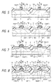
- Figs. 1 to 8 illustrate an embodiment in which the present invention is applied to a CMOS device.
- an N ⁇ -type well region 2 is formed by the drive-in diffusion of ion-implanted phosphorus or arsenic, while the P ⁇ -type well region 3 is formed by the drive-in diffusion of ion-implanted boron.
- the impurity concentration of each of the N ⁇ -type well region 2 and the P ⁇ -type well region 3 is approximately 2 x 10¹⁶ atoms/cm3. Further, as shown in Fig.
- the field insulator film 4 is formed by the thermal oxidation of the substrate 1 so as to define regions where elements are to be formed.
- a gate insulator film 6 which is about 15nm thick is formed on each of the element forming regions by the thermal oxidation of the substrate 1.
- an N-type impurity for example, As 7 or Sb 7 for adjusting the threshold voltages of both a P-channel MISFET and an N-channel MISFET is introduced into the surface of the substrate 1 by ion implantation at 60 keV and 5 x 10¹¹ atoms/cm2.
- diffusion coefficients are Sb « As « B.
- a polycrystalline silicon film 8A to constitute gate electrodes 8 is formed on the gate insulator films 6 overlying the substrate 1 to a thickness of about 200 nm by, for example, plasma CVD.
- a P-type impurity for example, boron is introduced into the polycrystalline silicon film 8A at 10 keV and 2 x 10¹⁵ atoms/cm2 so as to turn this film into the P+-type.
- a WSi2 film 8B to constitute the gate electrodes 8 is formed on the polycrystalline silicon film 8A to a thickness of about 200 nm by, for example, CVD.
- the WSi2 film 8B may well be a film of a refractory metal such as W, Mo, Ta, Ti or Pd or a film of any silicide of the refractory metal.
- a silicon oxide film 9 is further formed thereon at a thickness of about 80 nm by, for example, CVD.
- the silicon oxide film 9 serves to prevent As from entering the gate electrodes 8 at the ion implantation of the As which is performed later in order to form the source and drain regions of the N-channel MISFET Accordingly, this silicon oxide film is not especially required if the concentration of the boron in the P+-type polycrystalline silicon film 8A is high to the extent that this film 8A is not inverted into the N-type by the ion implantation at the step of forming the source and drain regions of the N-channel MISFET.
- the silicon oxide film 9, WSi2 film 8B and P+-type polycrystalline silicon film 8A are successively etched by etching which uses a mask made of a resist film not shown.
- Each of the gate electrodes 8 is made of a double-layer film which consists of the P+-type polycrystalline silicon film 8A and the WSi2 film 8B. After the etching, the mask made of the resist film is removed.
- a P-channel MISFET region (a region other than a region for forming the N-channel MISFET) is covered with a mask made of a resist film not shown, whereupon using the silicon oxide film 9 and the gate electrode 8 as a mask, P (phosphorus) is introduced into the N-channel MISFET forming region at, for example, 60 keV and 1 x 10¹³ atoms/cm2, thereby to form shallow ion-implanted layers of low impurity concentration 10A which constitute the source and drain regions of the N-channel MISFET.
- the mask made of the resist film is removed.
- a mask made of a resist film and covering the N-channel MISFET region is formed anew, and using the silicon oxide film 9 and the gate electrode 8 as a mask, boron is introduced into the P-channel MISFET forming region at, for example, 40 keV and 1 x 10¹³ atoms/cm2, thereby to form shallow ion-implanted layers of low impurity concentration 11A which constitute the source and drain regions of the P-channel MISFET After the ion implantation, the mask made of the resist film is removed.
- the resultant substrate is annealed at about 900°C to activate all of the impurity 7 for controlling the threshold voltages, the impurity of the N ⁇ -type regions 10A and the impurity of the P ⁇ -type regions 11A.
- the impurity 7 is hardly driven into the substrate 1 because the diffusion coefficient thereof is very small.
- a silicon oxide film having a thickness of about 400nm is formed on the whole surface of the substrate 1 by, for example, CVD, and it is etched back by reactive ion etching (RIE), thereby to form side walls 12 on both side surfaces of the gate electrodes 8.
- RIE reactive ion etching
- the P-channel MISFET region (on the N-type well 2) is covered with a mask made of a resist film not shown, and As is introduced into the N-channel MISFET forming region at 80 keV and approximately 5 x 10¹⁵ atoms/cm2 by ion implantation employing the gate electrode 8, silicon oxide film 9 and side walls 12 as a mask, thereby to form deep ion-implanted layers of high impurity concentration 10B which constitute the source and drain regions of the N-channel MISFET. After the ion implantation, the mask made of the resist film is removed.
- a mask made of a resist film and covering the N-channel MISFET region (the region other than the N-type well) is formed anew, and B (boron) is introduced into the P-channel MISFET region at 10 keV and approximately 2 x 10¹⁵ atoms/cm2 by ion implantation employing the gate electrode 8, silicon oxide film 9 and side walls 12 as a mask, thereby to form deep ion-implanted layers of high impurity concentration 11B which constitute the source and drain regions of the P-channel MISFET.
- the mask made of the resist film is removed.
- the N+-type regions 10B and the P ⁇ -type regions 11B are activated by annealing at about 950°C.
- the N-type impurity 7 for adjusting the threshold voltages spreads into the substrate 1 very little because the diffusion coefficient thereof is very small.
- an inter-layer insulator film 13 in which a phosphosilicate glass (PSG) film is stacked on a silicon oxide film deposited by, for example, plasma CVD; contact holes 14; and wiring 15 which comprises an aluminum film deposited by, for example, sputtering.
- PSG phosphosilicate glass
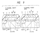
- a depletion layer spreading from each of the N ⁇ -type regions 10A or the P ⁇ -type regions 11A is illustrated in model fashion at letter D. It is assumed in Fig. 9 that the N ⁇ -type region 10A and the P ⁇ -type region 11A on the right sides are the drain regions, while the N ⁇ -type region 10A and the P ⁇ -type region 11A on the left sides are the source regions.
- the N-type impurity As or Sb is used as the impurity 7 for adjusting the threshold voltages.
- the depth of the junction formed between the P ⁇ -type well region 3 and the N ⁇ - or N-type region 7 by the impurity 7 becomes about 0.05 ⁇ m, which is very small as compared with the depth of a junction in the case of using the P-type impurity of boron as an impurity for adjusting threshold voltages.
- the junction part between the region 7 and the well region 3 does not further enlarge that part of the depletion layer of the drain region which is greatly spread. Accordingly, neither the punch-through between the source and the drain nor the change of the threshold voltage takes place.
- the N ⁇ -type well region 2 and the impurity 7 for adjusting the threshold voltage have the same conductivity type, so that a P-N junction is not defined in the channel region, and the spread of the depletion layer of the drain region is not promoted.
- the threshold voltage V th is expressed by: 0 ⁇ MS Difference between the work functions of the gate electrode and the substrate (silicon) 0 ⁇ F Fermi level of silicon Q B Quantity of charges in the substrate C OX Capacitance of the gate oxide film
- the impurity concentrations of the N ⁇ -type well region 2 and the P ⁇ -type well region 3 in this embodiment are both 2 x 10¹⁶ atoms/cm3, and the work function differences 0 ⁇ MS between them and the P+-type polycrystalline silicon film 8A are 0.92 eV and 0.18 eV, respectively.
- the values 2 0 ⁇ F of the N ⁇ -type well region 2 and the P ⁇ -type well region 3 are -0.74 eV and 0.74 eV, respectively.
- the value Q B /C OX of the N ⁇ -type well region 2 is -0.37 V, and that of the P ⁇ -type well region 3 is 0.37 V.
- an N-channel MISFET of the enhancement mode having a threshold voltage of about 0.6 V can be fabricated by forming the N ⁇ - or N-type region 7 in the channel region of the N-channel MISFET which has the gate electrode 8 including the P+-type polycrystalline silicon film as a part thereof. That is, the P+-type polycrystalline silicon film 8A is used as a part of the gate electrode 8 in order that the N-channel MISFET having the N ⁇ -type region 7 or N-type region 7 in the channel region may be rendered the enhancement mode, whereby an enhancement-mode N-channel MISFET having a threshold voltage of about 0.6 V can be fabricated.
- the threshold voltage is made too high merely by introducing the N-type impurity 7 into the channel region, and hence, the P+-type polycrystalline silicon film 8A is used as a part of the gate electrode 8, whereby an enhancement-mode P-channel MISFET having a threshold voltage of about -0.6 V can be fabricated.
- the N-channel MISFET and P-channel MISFET are used as, for example, elements which constitute the basic cell of a gate array.
- the gate electrode 8 of the N-channel MISFET and that of the P-channel MISFET are formed to be unitary, the interdiffusion of the impurities does not take place because both the members of the polycrystalline silicon film 8A constituting the gate electrodes are of the P+-type. That is, the threshold voltages do not fluctuate due to the interdiffusion of the impurities contained in the gate electrodes 8.
- a threshold voltage is controlled by the N-type impurity, for example, As or Sb of a channel region and the P+-type polycrystalline silicon film of a gate electrode, whereby in a P-channel MISFET, a P-N junction is not formed in the channel region, so that the spread of a depletion layer from a drain region is not promoted, and in an N-channel MISFET, even when a P-N junction is formed in the channel region, the depth thereof is as very small as about 0.05 ⁇ m from the surface of a substrate, so that the part of the depletion layer of a drain region having a great spread is not further enlarged. Accordingly, the fluctuations of the threshold voltages and punch-through become difficult to occur in both the P-channel MISFET and the N-channel MISFET, so that the short channels of the MISFETs can be attained.
- the N-type impurity for example, As or Sb of a channel region and the P+-type polycrystalline silicon film of a gate electrode
- the gate electrodes of the N-channel MISFET and the P-channel MISFET are both made of a poly-cide utilizing P+-type polycrystalline silicon, so that the problem of the inerdiffusion of impurities between the gate electrodes of the N-channel MISFET and the P-channel MISFET does not occur in the process of manufacture.
- an identical gate electrode can be shared by the P-channel and N-channel MISFETs, and a CMOS device suited to a high density of integration can be realized.
- the structure of the source or drain of a MISFET may be constructed only of a deep ion-implanted layer, or that of the drain may well be a DDD (Double Doped Drain) structure which is constructed of a diffused layer of low impurity concentration and a diffused layer of high impurity concentration.
- the material of a gate is not restricted to P-type polycrystalline silicon or a poly-cide utilizing P-type polycrystalline silicon, but it may be any material with which a plus work function difference is afforded relative to a semiconductor substrate.
Landscapes
- Metal-Oxide And Bipolar Metal-Oxide Semiconductor Integrated Circuits (AREA)
Applications Claiming Priority (2)
| Application Number | Priority Date | Filing Date | Title |
|---|---|---|---|
| JP229523/87 | 1987-09-16 | ||
| JP62229523A JPS6473676A (en) | 1987-09-16 | 1987-09-16 | Semiconductor integrated circuit device |
Publications (2)
| Publication Number | Publication Date |
|---|---|
| EP0308152A2 true EP0308152A2 (fr) | 1989-03-22 |
| EP0308152A3 EP0308152A3 (fr) | 1991-01-09 |
Family
ID=16893503
Family Applications (1)
| Application Number | Title | Priority Date | Filing Date |
|---|---|---|---|
| EP19880308388 Withdrawn EP0308152A3 (fr) | 1987-09-16 | 1988-09-12 | Circuit intégré MIS ainsi que son procédé de fabrication |
Country Status (3)
| Country | Link |
|---|---|
| EP (1) | EP0308152A3 (fr) |
| JP (1) | JPS6473676A (fr) |
| KR (1) | KR890005891A (fr) |
Cited By (5)
| Publication number | Priority date | Publication date | Assignee | Title |
|---|---|---|---|---|
| EP0414226A3 (fr) * | 1989-08-24 | 1991-04-03 | Nec Corporation | Transistor à effet de champ MOS avec parvoi latérale d'espacement |
| US5170232A (en) * | 1989-08-24 | 1992-12-08 | Nec Corporation | MOS field-effect transistor with sidewall spacers |
| EP0543268A3 (en) * | 1991-11-19 | 1993-08-11 | Texas Instruments Incorporated | Transistor device with a gate structure and method of forming the same |
| US5407839A (en) * | 1991-11-01 | 1995-04-18 | Seiko Epson Corporation | MOS manufacturing process having reduced gate insulator defects |
| WO1997036321A1 (fr) * | 1996-03-27 | 1997-10-02 | Advanced Micro Devices, Inc. | Procede de dopage separe des zones polygrille et drain-source |
Families Citing this family (8)
| Publication number | Priority date | Publication date | Assignee | Title |
|---|---|---|---|---|
| JP2776891B2 (ja) * | 1989-06-19 | 1998-07-16 | 株式会社日立製作所 | 半導体集積回路装置 |
| WO1997008752A1 (fr) * | 1995-08-25 | 1997-03-06 | Hitachi, Ltd. | Dispositif semiconducteur mis |
| JP4898013B2 (ja) * | 2001-04-04 | 2012-03-14 | セイコーインスツル株式会社 | 半導体装置 |
| JP2002313940A (ja) * | 2001-04-10 | 2002-10-25 | Seiko Instruments Inc | 半導体装置の製造方法 |
| JP4865152B2 (ja) * | 2001-06-19 | 2012-02-01 | セイコーインスツル株式会社 | 半導体装置の製造方法 |
| JP4898024B2 (ja) * | 2001-06-21 | 2012-03-14 | セイコーインスツル株式会社 | 半導体装置の製造方法 |
| JP2003007846A (ja) * | 2001-06-21 | 2003-01-10 | Seiko Instruments Inc | 半導体装置 |
| JP2009044002A (ja) * | 2007-08-09 | 2009-02-26 | Ricoh Co Ltd | 半導体装置及びそれを用いた温度検出装置 |
Family Cites Families (2)
| Publication number | Priority date | Publication date | Assignee | Title |
|---|---|---|---|---|
| US4242691A (en) * | 1978-09-18 | 1980-12-30 | Mitsubishi Denki Kabushiki Kaisha | MOS Semiconductor device |
| JPS61133656A (ja) * | 1984-12-03 | 1986-06-20 | Hitachi Ltd | 半導体装置およびその製造方法 |
-
1987
- 1987-09-16 JP JP62229523A patent/JPS6473676A/ja active Pending
-
1988
- 1988-08-31 KR KR1019880011148A patent/KR890005891A/ko not_active Withdrawn
- 1988-09-12 EP EP19880308388 patent/EP0308152A3/fr not_active Withdrawn
Cited By (6)
| Publication number | Priority date | Publication date | Assignee | Title |
|---|---|---|---|---|
| EP0414226A3 (fr) * | 1989-08-24 | 1991-04-03 | Nec Corporation | Transistor à effet de champ MOS avec parvoi latérale d'espacement |
| US5170232A (en) * | 1989-08-24 | 1992-12-08 | Nec Corporation | MOS field-effect transistor with sidewall spacers |
| US5407839A (en) * | 1991-11-01 | 1995-04-18 | Seiko Epson Corporation | MOS manufacturing process having reduced gate insulator defects |
| EP0543268A3 (en) * | 1991-11-19 | 1993-08-11 | Texas Instruments Incorporated | Transistor device with a gate structure and method of forming the same |
| WO1997036321A1 (fr) * | 1996-03-27 | 1997-10-02 | Advanced Micro Devices, Inc. | Procede de dopage separe des zones polygrille et drain-source |
| US6319804B1 (en) | 1996-03-27 | 2001-11-20 | Advanced Micro Devices, Inc. | Process to separate the doping of polygate and source drain regions in dual gate field effect transistors |
Also Published As
| Publication number | Publication date |
|---|---|
| EP0308152A3 (fr) | 1991-01-09 |
| JPS6473676A (en) | 1989-03-17 |
| KR890005891A (ko) | 1989-05-17 |
Similar Documents
| Publication | Publication Date | Title |
|---|---|---|
| US5254866A (en) | LDD CMOS with wider oxide sidewall on PMOS than NMOS | |
| KR0134756B1 (ko) | 반도체 장치 및 그 제조방법 | |
| US5278441A (en) | Method for fabricating a semiconductor transistor and structure thereof | |
| US4703552A (en) | Fabricating a CMOS transistor having low threshold voltages using self-aligned silicide polysilicon gates and silicide interconnect regions | |
| US5397715A (en) | MOS transistor having increased gate-drain capacitance | |
| US4411058A (en) | Process for fabricating CMOS devices with self-aligned channel stops | |
| US4849364A (en) | Semiconductor devices | |
| US4562638A (en) | Method for the simultaneous manufacture of fast short channel and voltage-stable MOS transistors in VLSI circuits | |
| US5294822A (en) | Polycide local interconnect method and structure | |
| EP0166167B1 (fr) | Procédé pour fabriquer un dispositif à semi-conducteur comportant des MISFETs à canal-n et à canal-p | |
| US5620922A (en) | Method for fabricating CMOS device having low and high resistance portions and wire formed from a single gate polysilicon | |
| US4698659A (en) | Stacked complementary metal oxide semiconductor inverter | |
| KR100420870B1 (ko) | Eeprom-반도체구조물의제조방법 | |
| EP0308152A2 (fr) | Circuit intégré MIS ainsi que son procédé de fabrication | |
| US4488348A (en) | Method for making a self-aligned vertically stacked gate MOS device | |
| US4784966A (en) | Self-aligned NPN bipolar transistor built in a double polysilicon CMOS technology | |
| US6027964A (en) | Method of making an IGFET with a selectively doped gate in combination with a protected resistor | |
| US5005066A (en) | Self-aligned NPN bipolar transistor built in a double polysilicon CMOS technology | |
| KR0172116B1 (ko) | 반도체 장치의 제조방법 | |
| EP0337481A2 (fr) | Dispositif semi-conducteur | |
| GB2088129A (en) | An integrated circuit mosfet and a method of making the same | |
| US5691564A (en) | Semiconductor device with high speed operation and high integration | |
| US5959334A (en) | Semiconductor memory device | |
| JP2845899B2 (ja) | 半導体集積回路装置の製造方法 | |
| WO2006018762A2 (fr) | Fabrication de cmos a passerelle double |
Legal Events
| Date | Code | Title | Description |
|---|---|---|---|
| PUAI | Public reference made under article 153(3) epc to a published international application that has entered the european phase |
Free format text: ORIGINAL CODE: 0009012 |
|
| AK | Designated contracting states |
Kind code of ref document: A2 Designated state(s): DE FR GB IT |
|
| PUAL | Search report despatched |
Free format text: ORIGINAL CODE: 0009013 |
|
| AK | Designated contracting states |
Kind code of ref document: A3 Designated state(s): DE FR GB IT |
|
| 17P | Request for examination filed |
Effective date: 19910708 |
|
| 17Q | First examination report despatched |
Effective date: 19930405 |
|
| STAA | Information on the status of an ep patent application or granted ep patent |
Free format text: STATUS: THE APPLICATION IS DEEMED TO BE WITHDRAWN |
|
| 18D | Application deemed to be withdrawn |
Effective date: 19930817 |