EP0308748A2 - Groupe électro-optique - Google Patents
Groupe électro-optique Download PDFInfo
- Publication number
- EP0308748A2 EP0308748A2 EP88114779A EP88114779A EP0308748A2 EP 0308748 A2 EP0308748 A2 EP 0308748A2 EP 88114779 A EP88114779 A EP 88114779A EP 88114779 A EP88114779 A EP 88114779A EP 0308748 A2 EP0308748 A2 EP 0308748A2
- Authority
- EP
- European Patent Office
- Prior art keywords
- substrate
- layer circuit
- housing
- electro
- housing base
- Prior art date
- Legal status (The legal status is an assumption and is not a legal conclusion. Google has not performed a legal analysis and makes no representation as to the accuracy of the status listed.)
- Withdrawn
Links
Images
Classifications
-
- H—ELECTRICITY
- H10—SEMICONDUCTOR DEVICES; ELECTRIC SOLID-STATE DEVICES NOT OTHERWISE PROVIDED FOR
- H10F—INORGANIC SEMICONDUCTOR DEVICES SENSITIVE TO INFRARED RADIATION, LIGHT, ELECTROMAGNETIC RADIATION OF SHORTER WAVELENGTH OR CORPUSCULAR RADIATION
- H10F77/00—Constructional details of devices covered by this subclass
- H10F77/50—Encapsulations or containers
-
- H—ELECTRICITY
- H10—SEMICONDUCTOR DEVICES; ELECTRIC SOLID-STATE DEVICES NOT OTHERWISE PROVIDED FOR
- H10W—GENERIC PACKAGES, INTERCONNECTIONS, CONNECTORS OR OTHER CONSTRUCTIONAL DETAILS OF DEVICES COVERED BY CLASS H10
- H10W90/00—Package configurations
-
- H—ELECTRICITY
- H10—SEMICONDUCTOR DEVICES; ELECTRIC SOLID-STATE DEVICES NOT OTHERWISE PROVIDED FOR
- H10H—INORGANIC LIGHT-EMITTING SEMICONDUCTOR DEVICES HAVING POTENTIAL BARRIERS
- H10H20/00—Individual inorganic light-emitting semiconductor devices having potential barriers, e.g. light-emitting diodes [LED]
- H10H20/80—Constructional details
- H10H20/85—Packages
- H10H20/8506—Containers
-
- H—ELECTRICITY
- H10—SEMICONDUCTOR DEVICES; ELECTRIC SOLID-STATE DEVICES NOT OTHERWISE PROVIDED FOR
- H10W—GENERIC PACKAGES, INTERCONNECTIONS, CONNECTORS OR OTHER CONSTRUCTIONAL DETAILS OF DEVICES COVERED BY CLASS H10
- H10W90/00—Package configurations
- H10W90/701—Package configurations characterised by the relative positions of pads or connectors relative to package parts
- H10W90/751—Package configurations characterised by the relative positions of pads or connectors relative to package parts of bond wires
- H10W90/754—Package configurations characterised by the relative positions of pads or connectors relative to package parts of bond wires between a chip and a stacked insulating package substrate, interposer or RDL
Definitions
- the invention relates to an electro-optical assembly according to the preamble of claim 1.
- the object of the invention is therefore to enable a high-precision mounting in the correct position of a layer circuit containing an optoelectric component in a metal housing containing optical components while dispensing with gluing and soldering.
- the object is achieved by an electro-optical module which is designed in accordance with the characterizing part of patent claim 1.
- Expedient developments of the electro-optical assembly according to the invention are described in claims 2 to 5 and a manufacturing method is described in claim 6.
- the electro-optical assembly according to the invention advantageously does not require subsequent cleaning, and furthermore, before the optoelectric component is inserted into the layer circuit, it can advantageously be produced by means of one of the customary manufacturing methods, so that the structure described is suitable for a large number of different layer circuits .
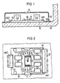
- GB is the metallic case back net, which is part of a metal housing in which a receiver module for the optical signal transmission via optical fibers as well as a mirror and an optical filter are installed.
- the integrated circuit IS with an optoelectric component OB is attached as part of the layer circuit SS on the ceramic substrate KS, which in turn is mounted on the housing base GB via a bracket HW with a z-shaped cross section.
- the brackets HW are firmly connected to edge strips RS of the substrate KS.
- the integrated circuit IS also contains an electrical amplifier arrangement. For this reason, the entire layer circuit is protected from electrical interference by a metallic shielding cap AK; an optical window FO in the form of a translucent glass pane is inserted in the shielding cap AK above the optoelectric component of the layer circuit SS.
- the z-shaped brackets are made of Vacon 10, this material has a coefficient of thermal expansion that lies between that of the ceramic substrate KS and that of the housing base GB.
- the brackets HW and the shield cap AK are connected to the housing base by means of welding spots that were generated by means of laser welding processes. The heat flow from the layer circuit via the ceramic substrate to the housing base and via the brackets and the welding points to the housing base has proven to be completely sufficient.
- the mounting brackets HW do not have to be the same size. While the first bracket HW1 extends almost over the entire right edge strip of the ceramic substrate KS, the second bracket HW2 covers only a small part of the left edge strip of the ceramic substrate. This ensures that this bracket is not with adjacent contact pads of the layer circuit SS in Be comes and causes a short circuit in the circuit.
- three capacitor chips CHP, CVC, CM are arranged on the substrate as part of the layer circuit, which are in electrical connection with the integrated circuit IS via contact strips and bonding wires.
- the manufacturing method for the electro-optical assembly according to FIGS. 1 and 2 will be explained below.
- the contact strips ST with contact pads for the capacitors CHP, CVC and CM as well as the metallized edge strips RS and a metallized carrier surface for the integrated circuit IS are produced on the ceramic substrate KS.
- the layer circuit is then equipped with the individual components, the components are attached, for example by thermal bonding, and the two holding brackets HW1, HW2 are attached to the edge strip RS.
- the layer circuit is then adjusted in the correct position on the housing base with a maximum error of approximately ⁇ 25 ⁇ m and the holding brackets are welded to the housing base using laser welding.
- the brackets are fixed so that the ceramic substrate KS is pressed onto the housing base to ensure the heat flow from the ceramic substrate to the housing base.
- a resistance welding process can also be used to generate the welding spots SP or a weld seam.
- the shielding cap AK is adjusted with the optical window FO above the layer circuit in such a way that the optical window lies above the optoelectric component OB of the integrated circuit and the shielding cap is also connected to the housing base by means of laser welding or resistance welding.
- the brackets are nickel-plated and partially gold-plated over the entire surface, and the shielding cap is also nickel-plated.
Landscapes
- Optical Couplings Of Light Guides (AREA)
Applications Claiming Priority (2)
| Application Number | Priority Date | Filing Date | Title |
|---|---|---|---|
| DE3732393 | 1987-09-25 | ||
| DE3732393 | 1987-09-25 |
Publications (2)
| Publication Number | Publication Date |
|---|---|
| EP0308748A2 true EP0308748A2 (fr) | 1989-03-29 |
| EP0308748A3 EP0308748A3 (fr) | 1990-07-04 |
Family
ID=6336908
Family Applications (1)
| Application Number | Title | Priority Date | Filing Date |
|---|---|---|---|
| EP88114779A Withdrawn EP0308748A3 (fr) | 1987-09-25 | 1988-09-09 | Groupe électro-optique |
Country Status (2)
| Country | Link |
|---|---|
| US (1) | US4906065A (fr) |
| EP (1) | EP0308748A3 (fr) |
Cited By (2)
| Publication number | Priority date | Publication date | Assignee | Title |
|---|---|---|---|---|
| WO1994017448A3 (fr) * | 1993-01-29 | 1994-11-10 | British Telecomm | Emballage pour dispositif optique |
| CN110828439A (zh) * | 2018-08-08 | 2020-02-21 | 光宝光电(常州)有限公司 | 光源装置及可携式通讯设备 |
Families Citing this family (3)
| Publication number | Priority date | Publication date | Assignee | Title |
|---|---|---|---|---|
| JPH0724112B2 (ja) * | 1988-12-19 | 1995-03-15 | ローム株式会社 | レーザダイオードユニットの取り付け方法 |
| US5233580A (en) * | 1988-12-19 | 1993-08-03 | Rohm Co., Ltd. | Laser diode unit welded to a mounting member by laser light |
| JP6763452B1 (ja) | 2019-04-15 | 2020-09-30 | 富士ゼロックス株式会社 | 発光装置、光学装置および情報処理装置 |
Family Cites Families (5)
| Publication number | Priority date | Publication date | Assignee | Title |
|---|---|---|---|---|
| US4346294A (en) * | 1979-07-05 | 1982-08-24 | Burr-Brown Research Corp. | Low profile optical coupling to planar-mounted optoelectronic device |
| FR2503458A1 (fr) * | 1981-04-02 | 1982-10-08 | Cit Alcatel | Tete optique |
| EP0184747A1 (fr) * | 1984-12-13 | 1986-06-18 | Heimann GmbH | Détecteur infrarouge |
| EP0213426A1 (fr) * | 1985-08-30 | 1987-03-11 | Siemens Aktiengesellschaft | Boîtier avec une partie de fond et une couverture extérieure pour un élément de circuit électrique |
| US4787696A (en) * | 1987-12-18 | 1988-11-29 | Gte Laboratories Incorporated | Mounting apparatus for optical fibers and lasers |
-
1988
- 1988-09-09 EP EP88114779A patent/EP0308748A3/fr not_active Withdrawn
- 1988-09-20 US US07/246,740 patent/US4906065A/en not_active Expired - Fee Related
Cited By (4)
| Publication number | Priority date | Publication date | Assignee | Title |
|---|---|---|---|---|
| WO1994017448A3 (fr) * | 1993-01-29 | 1994-11-10 | British Telecomm | Emballage pour dispositif optique |
| US5719974A (en) * | 1993-01-29 | 1998-02-17 | British Telecommunications Public Limited Company | Method for customizing optical device configuration after packaging and packaged optical device for use therewith |
| CN1061471C (zh) * | 1993-01-29 | 2001-01-31 | 英国电讯公司 | 光学器件封装和制造封装件的方法 |
| CN110828439A (zh) * | 2018-08-08 | 2020-02-21 | 光宝光电(常州)有限公司 | 光源装置及可携式通讯设备 |
Also Published As
| Publication number | Publication date |
|---|---|
| EP0308748A3 (fr) | 1990-07-04 |
| US4906065A (en) | 1990-03-06 |
Similar Documents
| Publication | Publication Date | Title |
|---|---|---|
| DE68926448T2 (de) | Bildsensor und verfahren zu dessen herstellung | |
| EP0308749A2 (fr) | Groupe électro-optique | |
| EP2008443B1 (fr) | Procede pour le montage d'un module de camera et module de camera | |
| DE69008480T2 (de) | Gehäuse für einen Festkörperbildsensor. | |
| DE69829703T2 (de) | Verfahren zum hermetischen Verschliessen einer optischen Faserdurchführung und hermetisch verschlossene Vorrichtung | |
| DE69519894T2 (de) | Photodetektor-Bauelement und Verfahren zu seiner Herstellung | |
| DE69118497T2 (de) | Kamerakopf für eine Festkörper-Bildaufnahme-Einrichtung und Verfahren zur Herstellung | |
| DE3138296C2 (fr) | ||
| DE3244867A1 (de) | Sende- und/oder empfangsvorrichtung fuer einrichtungen der elektrooptischen nachrichtenuebertragung | |
| DE19856663A1 (de) | Kontaktvorrichtung für ein an einer Fensterscheibe angeordnetes elektrisches Funktionselement | |
| DE4005324C2 (de) | Fotoelektrischer Wandler | |
| DE19932430A1 (de) | Opto-elektronische Baugruppe, Bauteile für diese Baugruppe sowie Verfahren zur Herstellung der Baugruppe | |
| EP0111263A2 (fr) | Appareil de transmission ou réception contenant une diode dans une monture | |
| DE69001548T2 (de) | Lichtemittierende halbleitervorrichtung. | |
| DE19807536A1 (de) | Verpackungsverfahren für optische Bauteile und Kollimator-Zusammenbauverfahren | |
| DE69213778T2 (de) | Verfahren zur Herstellung eines opto-elektronischen Bauteils | |
| EP0308748A2 (fr) | Groupe électro-optique | |
| DE2734798C2 (fr) | ||
| DE4106721A1 (de) | Anordnung zur ankopplung von lichtwellenleiterenden an empfangselemente | |
| DE69938272T2 (de) | Montierungsstruktur für Photohalbleitervorrichtung | |
| DE3433717A1 (de) | Verfahren zum koppeln optischer bauelemente und anordnung zur durchfuehrung des verfahrens | |
| DE3429282A1 (de) | Optoelektronisches modul | |
| DE102017210379A1 (de) | Bildsensormodul | |
| DE3307669A1 (de) | Koppelanordnung zwischen einem elektro-optischen und/oder opto-elektrischen halbleiterbauelement und einem lichtwellenleiter | |
| DE102005046164A1 (de) | Röntgendetektor |
Legal Events
| Date | Code | Title | Description |
|---|---|---|---|
| PUAI | Public reference made under article 153(3) epc to a published international application that has entered the european phase |
Free format text: ORIGINAL CODE: 0009012 |
|
| AK | Designated contracting states |
Kind code of ref document: A2 Designated state(s): DE FR GB IT |
|
| PUAL | Search report despatched |
Free format text: ORIGINAL CODE: 0009013 |
|
| AK | Designated contracting states |
Kind code of ref document: A3 Designated state(s): DE FR GB IT |
|
| 17P | Request for examination filed |
Effective date: 19901009 |
|
| STAA | Information on the status of an ep patent application or granted ep patent |
Free format text: STATUS: THE APPLICATION HAS BEEN WITHDRAWN |
|
| 18W | Application withdrawn |
Withdrawal date: 19910612 |
|
| R18W | Application withdrawn (corrected) |
Effective date: 19910612 |