EP0308953B1 - Detektor für geladene Teilchen - Google Patents
Detektor für geladene Teilchen Download PDFInfo
- Publication number
- EP0308953B1 EP0308953B1 EP88115653A EP88115653A EP0308953B1 EP 0308953 B1 EP0308953 B1 EP 0308953B1 EP 88115653 A EP88115653 A EP 88115653A EP 88115653 A EP88115653 A EP 88115653A EP 0308953 B1 EP0308953 B1 EP 0308953B1
- Authority
- EP
- European Patent Office
- Prior art keywords
- signal
- charged particle
- specimen
- electrode
- particle beam
- Prior art date
- Legal status (The legal status is an assumption and is not a legal conclusion. Google has not performed a legal analysis and makes no representation as to the accuracy of the status listed.)
- Expired
Links
- 239000002245 particle Substances 0.000 title claims description 27
- 230000005540 biological transmission Effects 0.000 claims description 7
- 230000001934 delay Effects 0.000 claims description 2
- 230000001678 irradiating effect Effects 0.000 claims description 2
- 239000011163 secondary particle Substances 0.000 claims 1
- 238000010894 electron beam technology Methods 0.000 description 14
- 230000004044 response Effects 0.000 description 7
- 238000000034 method Methods 0.000 description 6
- 238000010276 construction Methods 0.000 description 5
- 238000002955 isolation Methods 0.000 description 5
- 238000005259 measurement Methods 0.000 description 3
- 230000008054 signal transmission Effects 0.000 description 3
- 238000001514 detection method Methods 0.000 description 2
- 230000005684 electric field Effects 0.000 description 2
- 150000002500 ions Chemical group 0.000 description 1
- 239000000523 sample Substances 0.000 description 1
Images

Classifications
-
- H—ELECTRICITY
- H01—ELECTRIC ELEMENTS
- H01J—ELECTRIC DISCHARGE TUBES OR DISCHARGE LAMPS
- H01J37/00—Discharge tubes with provision for introducing objects or material to be exposed to the discharge, e.g. for the purpose of examination or processing thereof
- H01J37/02—Details
- H01J37/244—Detectors; Associated components or circuits therefor
-
- G—PHYSICS
- G01—MEASURING; TESTING
- G01R—MEASURING ELECTRIC VARIABLES; MEASURING MAGNETIC VARIABLES
- G01R31/00—Arrangements for testing electric properties; Arrangements for locating electric faults; Arrangements for electrical testing characterised by what is being tested not provided for elsewhere
- G01R31/28—Testing of electronic circuits, e.g. by signal tracer
- G01R31/302—Contactless testing
- G01R31/305—Contactless testing using electron beams
-
- H—ELECTRICITY
- H01—ELECTRIC ELEMENTS
- H01J—ELECTRIC DISCHARGE TUBES OR DISCHARGE LAMPS
- H01J2237/00—Discharge tubes exposing object to beam, e.g. for analysis treatment, etching, imaging
- H01J2237/244—Detection characterized by the detecting means
- H01J2237/24435—Microchannel plates
-
- H—ELECTRICITY
- H01—ELECTRIC ELEMENTS
- H01J—ELECTRIC DISCHARGE TUBES OR DISCHARGE LAMPS
- H01J2237/00—Discharge tubes exposing object to beam, e.g. for analysis treatment, etching, imaging
- H01J2237/244—Detection characterized by the detecting means
- H01J2237/2446—Position sensitive detectors
- H01J2237/24465—Sectored detectors, e.g. quadrants
-
- H—ELECTRICITY
- H01—ELECTRIC ELEMENTS
- H01J—ELECTRIC DISCHARGE TUBES OR DISCHARGE LAMPS
- H01J2237/00—Discharge tubes exposing object to beam, e.g. for analysis treatment, etching, imaging
- H01J2237/244—Detection characterized by the detecting means
- H01J2237/2448—Secondary particle detectors
-
- H—ELECTRICITY
- H01—ELECTRIC ELEMENTS
- H01J—ELECTRIC DISCHARGE TUBES OR DISCHARGE LAMPS
- H01J2237/00—Discharge tubes exposing object to beam, e.g. for analysis treatment, etching, imaging
- H01J2237/244—Detection characterized by the detecting means
- H01J2237/2449—Detector devices with moving charges in electric or magnetic fields
-
- H—ELECTRICITY
- H01—ELECTRIC ELEMENTS
- H01J—ELECTRIC DISCHARGE TUBES OR DISCHARGE LAMPS
- H01J2237/00—Discharge tubes exposing object to beam, e.g. for analysis treatment, etching, imaging
- H01J2237/245—Detection characterised by the variable being measured
- H01J2237/24507—Intensity, dose or other characteristics of particle beams or electromagnetic radiation
-
- H—ELECTRICITY
- H01—ELECTRIC ELEMENTS
- H01J—ELECTRIC DISCHARGE TUBES OR DISCHARGE LAMPS
- H01J2237/00—Discharge tubes exposing object to beam, e.g. for analysis treatment, etching, imaging
- H01J2237/245—Detection characterised by the variable being measured
- H01J2237/24564—Measurements of electric or magnetic variables, e.g. voltage, current, frequency
Definitions
- the present invention relates to a charged particle beam tester device and in which the improvement in high-speed response performance or characteristic is contemplated.
- an electron beam tester device (hereinafter referred to as EB tester device) utilizing a scanning electron microscope is used for measurement of internal voltages or potentials of large scale integrated (LSI) circuits.
- LSI large scale integrated
- a so-called stroboscopic type EB tester device using a pulsed electron beam is dominantly employed.
- an electric potential or voltage on a specimen is measured on the basis of a signal applied to the specimen and a secondary-electron signal generated from the specimen through irradiation of the specimen with an electron beam which is pulsed with an arbitrary width in synchronism with the signal applied to the specimen.
- the specimen potential changing at a high speed can be detected in a form converted into a version changing at a low speed.
- the pulse width of the electron beam determines the time precision of a voltage waveform measured. Therefore, the electron beam pulse width is selected to be 1/500 to 1/1000 of a pulse repetition period or approximately smaller than 1 ns.
- the EB tester device based on the stroboscopic method is effective for a specimen operating at a relatively short repetition period (smaller than 1 ⁇ s), for example, an LSI circuit such as a memory.
- the storoboscopic EB tester device brings upon a remarkable decrease in S/N since the duty of the electron beam becomes smaller than 1/104. As a result, a long time is required for measurement. Therefore, the stroboscopic method is not suited to the measurement for the logic LSI circuit.
- the above problem can be solved by employing an EB tester device which does not use the stroboscopic method but in which a specimen is irradiated with a DC electron beam and by developing a secondary-electron detecting system which can respond to the potential of a specimen operating at a high speed.
- a secondary-electron detector uses a scintillator and a photomultiplier in combination.
- MCP micro channel plate
- the MCP multiplies the incident secondary electrons by about 104 times by the action of the high electric field and the multiplied electrons reach an anode of the MCP.
- an output signal to be detected is obtained at a high voltage side. Therefore, an isolation amplifier is used to take out the output signal as an analog signal at a low voltage side.
- the time response of the MCP detector depends upon the frequency characteristic of the isolation amplifier.
- the improvement up to the time response (not larger than 1 ns) of the MCP may be technically possible by the selection of high-speed LSI circuits.
- a first problem concerns the behaviour of secondary electrons incident upon the front surface of the MCP, that is, a difference between travel times of the secondary electrons.
- Secondary electrons generated from a specimen emanate at every angle in accordance with the Lambert's cosine law.
- the secondary electrons are selected by a spherical energy filter (shown by reference numeral 2 in Fig. 1) and are incident upon a secondary-electron receiving surface 31 of the MCP 3 with voltage contrast information included. Therefore, secondary electrons e1 emanating from the peak of the spherical energy filter 2 and secondary electrons e2 emanating from the end or marginal portion of the filter 2 have different travel distances which result in a difference between arrival times.
- This arrival time difference is further increased when the energy distribution of secondary electrons generated is taken into consideration. This means that in the case where the specimen potential or voltage has a high-speed pulse change, a difference of travel times of secondary electrons appears as the dulled rise time of a pulse waveform detected, thereby making the faithful detection of a high-speed pulse waveform impossible.
- a second problem is an impedance matching. Since the frequency of a signal detected by the device is a high frequency in order of MHz to GHz, the device should be handled as a distributed constant circuit. Therefore, it is necessary to match the characteristic impedance Z a of the anode of the MCP with the characteristic impedance Z o of a transmission line extending from the anode to the isolation amplifier. If these impedances Z a and Z o are not equal to each other, a reflected wave is generated, thereby making the faithful detection of a high-speed pulse waveform impossible.
- the problem of the difference in travel time between secondary electrons and the problem of the impedance matching affect the high-speed response performance of the secondary-electron detector using the MCP.
- An object of the present invention is to provide an electron beam tester device with an excellent high-speed response performance which can reduce the above-mentioned difference in travel time between secondary electrons and can remove any reflected wave resulting from the mismatching of impedance.
- a charged particle beam tester device comprising means for generating a beam of charged particles, means for irradiating a specimen with the charged particle beam in a narrowly defined form, an MCP for detecting charged particles secondarily generated from the specimen, signal outputting means for transmitting therein a signal detected by the MCP and then outputting the signal, and processing means provided between the specimen and the signal outputting means for simultaneously outputting signals of secondary charged particles generated from the specimen at the same instant of time. It is preferable to make the characteristic impedance of a signal taking-out electrode of the MCP coincident with that of a transmission line.
- the secondary charged particle taking-out electrode in an anode of the MCP is provided with a vortex form and its characteristic impedance coincident with the characteristic impedance of the transmission line, and the secondary charged particle signal is taken out from an outer end portion of the vortex-shaped electrode.
- the secondary charged particle taking-out electrode in the anode of the MCP is divided into a plurality of concentric segments. Signals from the electrode segments are provided with predetermined delays by respective delaying elements and are thereafter summed to provide an output signal.
- the travel time t of secondary electrons can be calculated by the following equation (1):
- e/m is the specific charges of electrons
- V a the accelerating voltage of secondary electrons
- V o the initial velocity of secondary electrons
- X the travel distance
- the travel time of secondary electrons from a spherical grid of the energy filter to the secondary-electron receiving surface of the plate-like MCP can be calculated by use of the equation (1).
- the travel distance X c from the center of the spherical grid and the travel distance X e from the end or marginal portion of the spherical grid have a relation of X e > X c .
- the arrival times t c and t e of secondary electrons incident upon the MCP at central and end portions thereof have a relation of t e > t c .
- the above difference in arrival time is reduced in such a manner that the anode of the MCP is provided with a vortical electrode with a signal being taken out from an outer end portion of the vortical electrode so that a delay of propagation velocity is generated between the outer side of the electrode and the inner side thereof near the center to make the amount of that delay equal to the abovementioned difference in travel time between secondary electrons.
- the secondary-electron signal taken out from the outer end portion of the vortical electrode does not involve the difference in travel time between secondary electrons apparently.
- a stripe line is used to make the characteristic impedance of the vortex electrode coincide with that of the signal transmission line.
- the characteristic impedance Z of the stripe line can be calculated by the following equation:
- e r is the specific dielectric constant of a dielectric
- h the thickness of the dielectric
- W the width of the stripe line
- D the thickness of the stripe line.
- a secondary-electron signal free of any reflected wave can be taken out by calculating the characteristic impedance of the stripe line by means of the equation (2) and making it coincident with the characteristic impedance of the signal transmission line.
- a propagation delay t pd of the stripe line can be calculated by the following equation (3): Therefore, it is also possible to easily make the propagation delay coincident with the above-mentioned difference in travel time between secondary electrons.
- Fig. 1 is a view showing the construction of a first embodiment of the present invention.
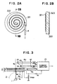
- Figs. 2A and 2B show the configuration or structure of an anode in a micro-channel plate (MCP) shown in Fig. 1. More especially, Fig. 2A is a plan view of the anode viewed from the side of a vortical electrode thereof and Fig. 2B is a cross section of the anode taken along line IIB-IIB in Fig. 2A.
- MCP micro-channel plate
- a primary electron beam e o emitted from an electron gun 9 is incident upon a specimen 1 by the action of an XY deflector 8 for permitting selective irradiation of any location on the specimen 1 with the primary electron beam e o and the action of an objective lense 7 for focusing the primary electron beam.
- Secondary electrons are generated from the specimen 1 and go straight toward a spherical energy filter 2.
- the specimen 1 is applied with any voltage. Therefore, the secondary electrons passed through the energy filter 2 become incident upon a secondary-electron receiving surface 31 of an MCP 3 with potential or voltage contrast information included therein.
- the secondary electrons e1 incident upon the vicinity of the center of the secondary-electron receiving surface 31 of the MCP 3 and the secondary electrons e2 incident upon an end or outer periphery portion thereof have different travel distances from the energy filter 2 and hence the arrival times of secondary-electron signals incident upon an anode 32 of the MCP 3 have fluctuations.
- the anode 32 has a structure as shown in Figs. 2A and 2B.
- the anode 32 includes an electrode 323 to be grounded on a rear surface and an electrode 321 for take-out of secondary-electron signal on a front surface with a dielectric 322 being sandwiched therebetween, and the electrode 321 is shaped into a vortex form starting from a center thereof and with a secondary-electron signal being taken out from an outer end portion of the vortex-shaped (vortical) electrode 321.
- the amount of propagation delay from the center of the electrode 321 to the end portion thereof is calculated in accordance with the equation (3) and is made equal to the difference in travel time between secondary electrons calculated in accordance with the equation (1).
- the secondary-electron signals are apparently incident upon or reach the signal taking-out point of the vortical electrode 321 of the anode 32 at the same instant of time.
- the characteristic impedance Z a of the vortical electrode 321 is made coincident with the characteristic impedance Z o of a transmission line 4. Therefore, no reflected wave is generated and hence the obtained secondary-electron signal includes a faithful voltage contrast signal.
- This secondary-electron signal is supplied to a signal detecting circuit 6 at a low voltage side through an impedance-matched high-speed isolation amplifier 5 and is taken out therefrom as a voltage contrast signal.
- reference symbol V mcp designates a high voltage source for the MCP 3
- symbol V a a DC power source for the anode 32.
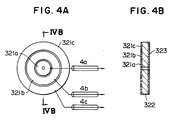
- Fig. 3 shows a main part of a detector according to the second embodiment and the other part not shown has the same construction as that shown in Fig. 1. Secondary electrons generated from a specimen 1 go straight toward a spherical energy filter 2 and is incident upon an MCP 3′, as shown in Fig. 3, with potential or voltage contrast information included therein.
- Secondary electrons e a incident upon the vicinity of the center of the MCP 3′, secondary electrons e c incident upon the outer periphery of the MCP 3′ and secondary electrons e b incident upon the intermediate portion therebetween have their travel distances or times which differ from each other depending on distances from the energy filter 2 to the front surface of the MCP 3′, and hence the arrival times of secondary electron signals incident upon an anode 32′ of the MCP 3′ have fluctuations.
- the anode 32′ of the MCP 3′ is divided into three concentric segments which are electrically isolated from each other.
- the characteristic impedance Z a of each anode segment is determined by use of the equation (2) so as to be equal to the characteristic impedance Z o of a transmission line 4a, 4b, 4c and the characteristic impedance Z o of a summing amplifier 10. As a result, any undesired reflected wave can be removed.
- Fig. 4A is a plan view of the anode 32′ and Fig. 4B is a cross section taken along line IVB-IVB in Fig. 4A.
- the anode 32′ is divided into segments 321a, 321b and 321c.
- Delaying elements d a and d b are connected to the anode segments 321a and 321b, respectively.
- the travel times t a , t b and t c of the secondary electrons e a , e b and e c calculated in accordance with the equation (1) like the first embodiment have a relation of t a ⁇ t b ⁇ t c .
- the anode of the MCP has been divided into three segments. A higher precision can be obtained with an increased number of anode segments.
- the output signal from the summing amplifier 10 is inputted to the isolation amplifier in the same manner as that in the first embodiment and a faithful voltage contrast signal is taken out by the signal detecting circuit.
- any fluctuation of travel times of secondary charged particles generated from a specimen can be removed and the impedance matching of a signal transmission line is possible.
Landscapes
- Engineering & Computer Science (AREA)
- General Engineering & Computer Science (AREA)
- Physics & Mathematics (AREA)
- General Physics & Mathematics (AREA)
- Chemical & Material Sciences (AREA)
- Analytical Chemistry (AREA)
- Measurement Of Radiation (AREA)
- Electron Tubes For Measurement (AREA)
- Tests Of Electronic Circuits (AREA)
Claims (6)
- Prüfgerät mit einem Strahl von geladenen Teilchen mit
Einrichtungen (9) zum Erzeugen eines Strahls von geladenen Teilchen;
Einrichtungen (7, 8) zum Bestrahlen einer Probe (1) mit dem Strahl von geladenen Teilchen in einer eng definierten Form;
einer Mikrokanalplatte (3, 3') zum Erfassen von geladenen Teilchen, welche sekundär von der Probe erzeugt worden sind;
Signalausgangseinrichtungen (4, 4a - 4c, 5, 6) zum Übertragen eines durch die Mikrokanalplatte erfaßten Signals und zum anschließenden Ausgeben des Signals; und
Verarbeitungseinrichtungen (32, 32', da, db, 10), welche zwischen der Probe und den Signalausgangseinrichtungen angeordnet sind, zum gleichzeitigen Ausgeben von Signalen von sekundären Teilchen, welche von der Probe zum gleichen Zeitpunkt erzeugt worden sind. - Prüfgerät mit einem Strahl von geladenen Teilchen gemäß Anspruch 1 mit Einrichtungen (2) zum Auswählen der Energie der von der Probe (1) erzeugten sekundären geladenen Teilchen, wobei die energieausgewählten sekundären geladenen Teilchen zu der Mikrokanalplatte (3, 3') übertragen werden.
- Prüfgerät mit einem Strahl von geladenen Teilchen gemäß Anspruch 1, bei welchem die Verarbeitungseinrichtungen derart ausgebildet sind, daß eine Elektrode (321) zur Entnahme des Signals der sekundären geladenen Teilchen in einer Anode (32) der Mikrokanalplatte (3) zu einer Spairalform geformt ist und ein Signal der sekundären geladenen Teilchen von einem äußeren Endabschnitt der spiralförmigen Elektrode entnommen wird.
- Prüfgerät mit einem Strahl von geladenen Teilchen gemäß Anspruch 3, bei welchem die charakteristische Impedanz der spiralförmigen Elektrode (321) mit derjenigen einer Übertragungslinie (4) für die Signalentnahme abgestimmt ist.
- Prüfgerät mit einem Strahl von geladenen Teilchen gemäß Anspruch 1, bei welchem die Verarbeitungseinrichtungen derart ausgebildet sind, daß eine Elektrode zur Entnahme der sekundären geladenen Teilchen in einer Anode (32') der Mikrokanalplatte (3') in eine Vielzahl von konzentrischen Segmenten (321a-321c) aufgeteilt ist und Signale von den jeweiligen Elektrodensegmenten nach bestimmten Zeitverzögerungen summiert werden.
- Prüfgerät mit einem Strahl von geladenen Teilchen gemäß Anspruch 5, bei welchem die charakteristische Impedanz des Elektrodensegments (321a-321c) mit derjenigen einer Übertragungslinie (4a-4c) für die Signalentnahme abgestimmt ist.
Applications Claiming Priority (2)
| Application Number | Priority Date | Filing Date | Title |
|---|---|---|---|
| JP238918/87 | 1987-09-25 | ||
| JP62238918A JPS6482445A (en) | 1987-09-25 | 1987-09-25 | Charged particle detector |
Publications (2)
| Publication Number | Publication Date |
|---|---|
| EP0308953A1 EP0308953A1 (de) | 1989-03-29 |
| EP0308953B1 true EP0308953B1 (de) | 1992-03-11 |
Family
ID=17037209
Family Applications (1)
| Application Number | Title | Priority Date | Filing Date |
|---|---|---|---|
| EP88115653A Expired EP0308953B1 (de) | 1987-09-25 | 1988-09-23 | Detektor für geladene Teilchen |
Country Status (4)
| Country | Link |
|---|---|
| US (1) | US4868394A (de) |
| EP (1) | EP0308953B1 (de) |
| JP (1) | JPS6482445A (de) |
| DE (1) | DE3869031D1 (de) |
Families Citing this family (15)
| Publication number | Priority date | Publication date | Assignee | Title |
|---|---|---|---|---|
| US4958079A (en) * | 1989-02-21 | 1990-09-18 | Galileo Electro-Optics Corps. | Detector for scanning electron microscopy apparatus |
| US4988867A (en) * | 1989-11-06 | 1991-01-29 | Galileo Electro-Optics Corp. | Simultaneous positive and negative ion detector |
| JP2567736B2 (ja) * | 1990-11-30 | 1996-12-25 | 理化学研究所 | イオン散乱分析装置 |
| EP0490154A3 (en) * | 1990-12-07 | 1992-09-30 | Siemens Aktiengesellschaft | Method for determining the charge of a sample region |
| DE69223088T2 (de) * | 1991-06-10 | 1998-03-05 | Fujitsu Ltd | Apparat zur Musterüberprüfung und Elektronenstrahlgerät |
| US5557105A (en) * | 1991-06-10 | 1996-09-17 | Fujitsu Limited | Pattern inspection apparatus and electron beam apparatus |
| US5391874A (en) * | 1993-08-17 | 1995-02-21 | Galileo Electro-Optics Corporation | Flexible lead assembly for microchannel plate-based detector |
| JP3431228B2 (ja) * | 1993-09-21 | 2003-07-28 | 株式会社東芝 | 荷電粒子検出装置及び荷電粒子照射装置 |
| US5475228A (en) * | 1994-11-28 | 1995-12-12 | University Of Puerto Rico | Unipolar blocking method and apparatus for monitoring electrically charged particles |
| JPH09106777A (ja) * | 1995-10-11 | 1997-04-22 | Hamamatsu Photonics Kk | 電子顕微鏡用電子増倍器 |
| US7531812B2 (en) * | 2003-10-27 | 2009-05-12 | Politechnika Wroclawska | Method and system for the directional detection of electrons in a scanning electron microscope |
| JP4429750B2 (ja) * | 2004-01-30 | 2010-03-10 | 日本電子株式会社 | マイクロチャンネルプレートを用いた検出器 |
| US7148485B2 (en) * | 2004-05-28 | 2006-12-12 | Hewlett-Packard Development Company, L.P. | Low-energy charged particle detector |
| US20080017811A1 (en) * | 2006-07-18 | 2008-01-24 | Collart Erik J H | Beam stop for an ion implanter |
| CN105470093B (zh) * | 2015-11-30 | 2017-07-14 | 中国科学院长春光学精密机械与物理研究所 | 双角电荷分割型阳极 |
Family Cites Families (6)
| Publication number | Priority date | Publication date | Assignee | Title |
|---|---|---|---|---|
| US29500A (en) * | 1860-08-07 | Machine foe | ||
| US3626184A (en) * | 1970-03-05 | 1971-12-07 | Atomic Energy Commission | Detector system for a scanning electron microscope |
| USRE29500E (en) | 1970-08-31 | 1977-12-20 | Max-Planck-Gesellschaft Zur Forderung Der Wissenschaften E.V. | Scanning charged beam particle beam microscope |
| GB1447983A (en) * | 1973-01-10 | 1976-09-02 | Nat Res Dev | Detector for electron microscopes |
| FR2220871B1 (de) * | 1973-07-27 | 1978-01-20 | Jeol Ltd | |
| DE3236273A1 (de) * | 1982-09-30 | 1984-04-05 | Siemens AG, 1000 Berlin und 8000 München | Spektrometerobjektiv mit parallelen objektiv- und spektrometerfeldern fuer die potentialmesstechnik |
-
1987
- 1987-09-25 JP JP62238918A patent/JPS6482445A/ja active Pending
-
1988
- 1988-09-23 DE DE8888115653T patent/DE3869031D1/de not_active Expired - Lifetime
- 1988-09-23 EP EP88115653A patent/EP0308953B1/de not_active Expired
- 1988-09-23 US US07/248,378 patent/US4868394A/en not_active Expired - Fee Related
Also Published As
| Publication number | Publication date |
|---|---|
| EP0308953A1 (de) | 1989-03-29 |
| JPS6482445A (en) | 1989-03-28 |
| US4868394A (en) | 1989-09-19 |
| DE3869031D1 (de) | 1992-04-16 |
Similar Documents
| Publication | Publication Date | Title |
|---|---|---|
| US4868394A (en) | Charged particle detector | |
| Brown | An improved time-of-flight ion charge state diagnostic | |
| US5990483A (en) | Particle detection and particle detector devices | |
| JP3836519B2 (ja) | 電子検出器 | |
| EP0389397B1 (de) | Apparat zum Prüfen von Unterbrechungen/Kurzschlüssen bei kapazitiv gekoppelten Netzen in Substraten unter Verwendung von Elektronenstrahlen | |
| WO1992019367A1 (en) | Time-of-flight mass spectrometer with an aperture enabling tradeoff of transmission efficiency and resolution | |
| EP0488067B1 (de) | Ionenstreuungsspektrometer | |
| EP0233123B1 (de) | Apparatur für pulsierende Elektronenstrahlen | |
| US4958079A (en) | Detector for scanning electron microscopy apparatus | |
| Menzel et al. | Secondary electron detection systems for quantitative voltage measurements | |
| EP0559202B1 (de) | Sekundärionenmassenspektrometer zur Analyse positiv und negativ geladener Ionen | |
| US3920990A (en) | Device for analysing a surface layer by means of ion scattering | |
| EP0304525A1 (de) | Gepulste mikrofokussierte Ionenstrahlen | |
| Thurgate et al. | An Auger photoelectron coincidence spectrometer | |
| Sefkow et al. | Fast Faraday cup to measure neutralized drift compression in intense ion charge bunches | |
| US5026988A (en) | Method and apparatus for time of flight medium energy particle scattering | |
| Murray et al. | A low-energy MHz repetition rate short-pulse electron gun | |
| JPH071282B2 (ja) | アツト・アンペア計 | |
| Knibbeler et al. | Novel two‐dimensional position‐sensitive detection system | |
| Seah et al. | Quantitative aes: the problems of the energy dependent phase shift and modulation amplitude and of the non-ideal behaviour of the channel electron multiplier | |
| JP4130904B2 (ja) | 平行磁場型ラザフォード後方散乱分析装置 | |
| WO1998036268A1 (en) | Charged particle analysis | |
| Dinnis et al. | The time-of-flight voltage contrast spectrometer: first results | |
| US4882480A (en) | Apparatus for detecting the position of incidence of particle beams including a microchannel plate having a strip conductor with combed teeth | |
| US4709140A (en) | High speed light detection tube |
Legal Events
| Date | Code | Title | Description |
|---|---|---|---|
| PUAI | Public reference made under article 153(3) epc to a published international application that has entered the european phase |
Free format text: ORIGINAL CODE: 0009012 |
|
| 17P | Request for examination filed |
Effective date: 19880923 |
|
| AK | Designated contracting states |
Kind code of ref document: A1 Designated state(s): DE GB |
|
| 17Q | First examination report despatched |
Effective date: 19910605 |
|
| GRAA | (expected) grant |
Free format text: ORIGINAL CODE: 0009210 |
|
| AK | Designated contracting states |
Kind code of ref document: B1 Designated state(s): DE GB |
|
| REF | Corresponds to: |
Ref document number: 3869031 Country of ref document: DE Date of ref document: 19920416 |
|
| PLBE | No opposition filed within time limit |
Free format text: ORIGINAL CODE: 0009261 |
|
| STAA | Information on the status of an ep patent application or granted ep patent |
Free format text: STATUS: NO OPPOSITION FILED WITHIN TIME LIMIT |
|
| 26N | No opposition filed | ||
| PGFP | Annual fee paid to national office [announced via postgrant information from national office to epo] |
Ref country code: GB Payment date: 19940913 Year of fee payment: 7 |
|
| PGFP | Annual fee paid to national office [announced via postgrant information from national office to epo] |
Ref country code: DE Payment date: 19941025 Year of fee payment: 7 |
|
| PG25 | Lapsed in a contracting state [announced via postgrant information from national office to epo] |
Ref country code: GB Effective date: 19950923 |
|
| GBPC | Gb: european patent ceased through non-payment of renewal fee |
Effective date: 19950923 |
|
| PG25 | Lapsed in a contracting state [announced via postgrant information from national office to epo] |
Ref country code: DE Effective date: 19960601 |