EP0309038A1 - Schaltung zur Regenerierung des Trägers für Datenübertragungsanordnungen - Google Patents
Schaltung zur Regenerierung des Trägers für Datenübertragungsanordnungen Download PDFInfo
- Publication number
- EP0309038A1 EP0309038A1 EP88202004A EP88202004A EP0309038A1 EP 0309038 A1 EP0309038 A1 EP 0309038A1 EP 88202004 A EP88202004 A EP 88202004A EP 88202004 A EP88202004 A EP 88202004A EP 0309038 A1 EP0309038 A1 EP 0309038A1
- Authority
- EP
- European Patent Office
- Prior art keywords
- phase
- states
- constellation
- oscillator
- zones
- Prior art date
- Legal status (The legal status is an assumption and is not a legal conclusion. Google has not performed a legal analysis and makes no representation as to the accuracy of the status listed.)
- Granted
Links
Images


Classifications
-
- H—ELECTRICITY
- H03—ELECTRONIC CIRCUITRY
- H03L—AUTOMATIC CONTROL, STARTING, SYNCHRONISATION OR STABILISATION OF GENERATORS OF ELECTRONIC OSCILLATIONS OR PULSES
- H03L7/00—Automatic control of frequency or phase; Synchronisation
- H03L7/06—Automatic control of frequency or phase; Synchronisation using a reference signal applied to a frequency- or phase-locked loop
- H03L7/08—Details of the phase-locked loop
- H03L7/085—Details of the phase-locked loop concerning mainly the frequency- or phase-detection arrangement including the filtering or amplification of its output signal
- H03L7/087—Details of the phase-locked loop concerning mainly the frequency- or phase-detection arrangement including the filtering or amplification of its output signal using at least two phase detectors or a frequency and phase detector in the loop
-
- H—ELECTRICITY
- H04—ELECTRIC COMMUNICATION TECHNIQUE
- H04L—TRANSMISSION OF DIGITAL INFORMATION, e.g. TELEGRAPHIC COMMUNICATION
- H04L27/00—Modulated-carrier systems
- H04L27/18—Phase-modulated carrier systems, i.e. using phase-shift keying
- H04L27/22—Demodulator circuits; Receiver circuits
- H04L27/227—Demodulator circuits; Receiver circuits using coherent demodulation
- H04L27/2271—Demodulator circuits; Receiver circuits using coherent demodulation wherein the carrier recovery circuit uses only the demodulated signals
- H04L27/2273—Demodulator circuits; Receiver circuits using coherent demodulation wherein the carrier recovery circuit uses only the demodulated signals associated with quadrature demodulation, e.g. Costas loop
-
- H—ELECTRICITY
- H04—ELECTRIC COMMUNICATION TECHNIQUE
- H04L—TRANSMISSION OF DIGITAL INFORMATION, e.g. TELEGRAPHIC COMMUNICATION
- H04L27/00—Modulated-carrier systems
- H04L27/0014—Carrier regulation
- H04L2027/0044—Control loops for carrier regulation
- H04L2027/0063—Elements of loops
- H04L2027/0067—Phase error detectors
-
- H—ELECTRICITY
- H04—ELECTRIC COMMUNICATION TECHNIQUE
- H04L—TRANSMISSION OF DIGITAL INFORMATION, e.g. TELEGRAPHIC COMMUNICATION
- H04L27/00—Modulated-carrier systems
- H04L27/0014—Carrier regulation
- H04L2027/0044—Control loops for carrier regulation
- H04L2027/0071—Control of loops
- H04L2027/0075—Error weighting
Definitions
- the invention relates to a circuit for recovering the carrier wave of a digitally modulated wave of phase symmetry 2 ⁇ / M, where M is the order of the symmetry of the constellation of states, provided with automatic acquisition means and fast comprising a voltage controllable oscillator having an output delivering said carrier wave and a control input to which an error signal ⁇ ( ⁇ ) is applied in order to modify the phase of the oscillator and enslave it to that of the digitally modulated wave, this being introduced: . on a first track comprising in series: a demodulator receiving the modulated wave and the output of the oscillator, the demodulator being followed by a low-pass filter which delivers a filtered signal X, .
- a second channel comprising in series: - a 90 ° phase shifter of the oscillator signal, a demodulator receiving the modulated wave and the output of the phase shifter, the demodulator being followed by a low-pass filter which delivers a filtered signal Y, the two channels entering with a basic clock H (symbol clock recovered), in a phase comparison device which determines a comparison signal and validates it using a sampling clock with variable cadence which reproduces the basic clock H by excluding certain edges, the comparison signal being memorized then introduced into an amplifier filter which delivers the error signal ⁇ ( ⁇ ) controlling the oscillator, the graphic representation of the states of a constellation being defined in polar coordinates by the function F (A, ⁇ ) where A is the amplitude and ⁇ the phase of cha that point of the constellation, and ⁇ being the phase difference between the modulated wave received and the point of the corresponding constellation.
- the invention also relates to devices where a carrier wave recovery circuit finds its application, such as digital transmission devices, in particular those for which information, after having been transmitted by modulation of an electromagnetic wave is restored. by coherent demodulation. These devices find their application in data transmission modems, radio-relay systems, spatial or optical communications systems in the case of heterodyne links.
- the phase of the carrier wave is generally restored using an oscillator placed in a carrier recovery loop.
- This oscillator is voltage controlled by a filtered version of the output signal from a phase comparator which detects the phase difference between the oscillator and the transmission carrier wave.
- phase difference between the oscillator and the carrier wave must be limited to small values.
- the noise band of the recovery loop is then reduced using narrow low-pass filtering. This reduction results in low phase noise, and also a considerable reduction in the acquisition range.
- acquisition aid devices are used.
- frequency discriminators are commonly used which generate a voltage which depends on the frequency difference between the oscillator and the carrier wave such as that described in French Patent No. 2,552,959 issued on October 25, 1985.
- This patent relates to a carrier recovery circuit for modulations digital symmetry 2 ⁇ / M in which a variable rate sampling of the output of the phase comparator transforms it into a frequency discriminator. This property is obtained by eliminating the zero transitions of the phase comparator output which occur when the phase error between the oscillator and the carrier wave is equal to + , where k and M are whole numbers.
- the frequency discriminator described in this patent, has drawbacks, its gain being degraded, because it remains on the sampled output of the phase comparator transitions by zero which are taken into account, and which do not correspond to a zero phase error. Indeed, this frequency discriminator generates a sampling clock, from a base clock H, in which certain active edges of the latter are eliminated. This elimination occurs when zero transitions are detected for which the phase difference between the oscillator and the carrier wave is equal to + .
- the object of the invention is therefore to avoid this degradation by eliminating the consideration of all the tran zero unwanted positions.
- the carrier wave recovery circuit has a phase comparison device which operates alternately as a phase detector and as a frequency detector and for this comprises means for selecting the points received using selection zones adjoining certain states of the constellation, the zones forming portions of rings being determined by the intersection: - first angular sectors (- ⁇ , + ⁇ ) corresponding to a phase difference ampli between the modulated wave received and the point of the corresponding constellation, such as absolute value of ⁇ ⁇ where ⁇ is a predetermined terminal, each sector having an axis of symmetry passing through the diagonal states of the constellation, these areas adjoining the diagonal states of the constellation for which there exists in a quarter plane only one state having a given amplitude A, -with second border circles, centered on the origin of the constellation, of radius , equidistant from two consecutive circles joining states, one passing through the states with constant amplitude A1 and the other passing through the states with constant amplitude A2 consecutive, thus forming rings, the point of origin
- phase difference such that the absolute value of ⁇ ⁇ is taken into account, i.e. the zone is selected, when the signs of the phase difference are the same for these two adjacent states.
- the data X and Y are used to address a memory which contains the information of membership or not of the point received in one of the selected zones as well as the amplitude and the sign of the error which relate to it.
- This device is based on the storage of the error signal when the absolute value of the phase difference ⁇ exceeds a certain value. This storage takes place in flip-flops whose output data remain stable between two zero transitions recognized as valid. This error signal gives information on the sign of the frequency difference between the oscillator and the carrier wave. This storage is carried out when the phase difference at the output of the comparator is located in the defined selection areas.
- This carrier wave recovery circuit uses a phase comparator which has the following properties: - its characteristic is canceled for a zero phase difference; - its characteristic is periodic with a period 2 ⁇ / M where M is the order of symmetry of the modulation.
- the invention finds its application for digital modulations of phase symmetry 2 ⁇ / M where M is the order of symmetry of the constellation.
- M is the order of symmetry of the constellation.
- a 4-state phase modulation has a 4-order symmetry, for an 8-state phase modulation the symmetry is of an 8 order, for a phase and amplitude modulation of two carriers in quadrature MAQ 16 la symmetry is of order 4.
- the invention has its decisive advantages in the case of amplitude and phase modulation with a large number of states, of type 2 n (n integer), for example MAQ 64, MAQ 256. It also has advantages in the amplitude and phase modulations for which the phase differences between certain points of the constellation are less than the 2 ⁇ / M symmetry.
- MAQ 64 modulation the symmetry is ⁇ / 2, but the phase difference between the states (+1, +1) and (+ 1, + 5) is ⁇ / 4-arc tan (1/5) therefore less than ⁇ / 2.
- the digitally modulated wave will be able to present all the points of the constellation.
- the invention therefore eliminates all the points received which are liable to cause an incorrect acquisition and only uses points which are capable of causing a correct acquisition.
- the carrier wave recovery circuit has means for selecting the points received using zones located around or adjoining certain states of the constellation.
- This selection is made by determining the membership or non-membership of the points received in zones for which any point received in these zones has a phase difference with the transmitted point, such that the absolute value of this phase difference remains less than 2k ⁇ / M near a predetermined limit, which eliminates zero transitions at k ⁇ / M.
- the invention constructs a phase comparison device which is inserted into a circuit for recovering a carrier wave.
- the digitally modulated wave is introduced simultaneously on two demodulators, one also receiving the output of the oscillator and the other this same output but after having crossed a phase shifter of ⁇ / 2 and respectively delivering the demodulated signals X1 and Y1. These are filtered and provide the signals X (in phase) and Y (in quadrature) respectively.
- the ifs X and Y signals are introduced into the phase comparison device and are used to address a memory.
- the X and Y data are coded on a certain number of bits depending on the precision with which the selection areas must be determined.
- the phase comparison device comprises two analog-digital converters placed respectively on the channels in phase and in quadrature in order to receive the Cartesian coordinates X and Y of the point received, the two converters delivering data which address a memory whose output delivers p bits, one of the bits being a bit belonging to the point received in one of the selected zones which activates an input of a logic gate OR the other input of which receives an external latching / unhooking signal, the output of the OR gate entering an AND gate with the base clock H in order to remove the edges when, in the acquisition mode, the received point is not in a selected area, and to validate all the edges in the permanent state, in order to constitute the sampling clock which activates p-1 flip-flops which receive the p-1 bits from the memory, the outputs of the flip-flops actuating a digital-analog converter which delivers the error signal which acts on the oscillator through the amplifier filter.
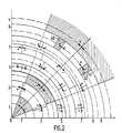
- a boundary circle 40 equidistant from the two states is defined such that its radius is .
- a point can be received with any phase and be located on one side or the other of the state of the constellation, which defines a phase difference.
- One affects the positive sign if the phase of the received point is higher than that of the point of the constellation and the negative sign in the opposite case.
- One thus carries out a cutting out in polar coordinates of all the plane of the constellation.
- a rotation in one direction or the other characterizes the sign of the phase difference.
- the invention determines a terminal ⁇ for the phase difference ⁇ beyond which the point received is no longer used to synchronize the local carrier of the recovery circuit with the transmitted carrier.
- the areas which are determined by the invention are thus bounded by the border circles and by the sector (- ⁇ , + ⁇ ).
- the border circles 40 and 31 and the segments 32 and 34 there is a selection area, affected by a negative sign, bounded by the border circles 40 and 31 and the segments 32 and 34.
- the states ( ⁇ 1, ⁇ 1), ( ⁇ 3, ⁇ 3), ( ⁇ 7, ⁇ 7) have a symmetry equal to ⁇ / 2 for the entire MAQ 64 constellation. They are therefore perfectly determined in a quarter plane of the constellation. On the other hand there exists, in a quarter of plan, a diagonal state (+5, +5) which has a symmetry lower than ⁇ / 2 and cannot therefore be differentiated from the states (+7, +1) and (+1, +7). There is therefore no selection area in the ring passing through these three states.
- the invention thus determines three selection zones located in the rings defined around the diagonal states (1,1), (3,3), (7,7). They are represented by hatched surfaces in FIG. 1.
- the incident signal represented in Cartesian data by X and Y, makes it possible to determine the membership or non-membership of the point received in one of these areas.
- the X and Y data are coded on several bits according to the precision sought. If the point received is located in an element of the selection area such as 35, it will be assigned sign information (here the negative sign) and amplitude information characterizing, if necessary, its distance from the state (3.3) to produce the correct phase correction.
- sign information here the negative sign
- amplitude information characterizing, if necessary, its distance from the state (3.3) to produce the correct phase correction.
- a simple coding can consist of two bits, one for the sign and the other for the amplitude of the correction then constant for the whole area.
- a more elaborate coding can consist of three bits, one for the sign and the other two bits to define several amplitudes of correction according to the position of the point 35 in the selection area.
- This coding is performed for all areas of selection.
- the terminals ⁇ can also be different for each of the zones.
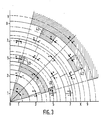
- FIG. 2 represents the same situation as that of FIG. 1 but represented with a larger terminal ⁇ .
- This zone is superimposed on the zone with negative sign adjoining state (7, 5).
- the two zones with phase difference of negative sign overlapping, any received point being in the hatched zone 42 unambiguously determines the sign of the correction.
- a zone 43 is attached to the state (5, 7) with a positive correction.
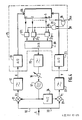
- FIG. 4 represents the block diagram of the carrier wave recovery circuit.
- the digitally modulated wave arrives at the input connection 5 and is subdivided into two channels 10 and 20 respectively in phase and in quadrature with the wave of the oscillator 17. This delivers its signal directly to the demodulator 11 of the phase channel, and also to the demodulator 21 of the quadrature channel through the phase shifter of ⁇ / 2 24.
- the outputs of the demodulators 11 and 21 are filtered respectively in the low-pass filters 12 and 22 having the output signal respectively X and Y.
- These signals enter the phase comparison device 25, respectively in two analog-digital converters 13, 23, which deliver data which addresses a PROM memory 26. This delivers p bits of which p-1 bits are stored in flip-flops 271, 272 ...
- the p th bit p p determines whether or not the received point determined by its X, Y coordinates belongs to a selected selection area.
- the output of the OR logic gate 28 enters an AND logic gate 29 with the base clock H.
- This signal H1 constitutes the clock for the flip-flops 271 to 27 p-1 .
- All the outputs of the p-1 flip-flops enter a digital-analog converter 30 which delivers a signal which passes through a low-pass filter 15 and then into an amplifier. tor 16 to supply a control signal ⁇ ( ⁇ ) which controls the oscillator 17. It is obviously possible for a person skilled in the art to reverse the logic state of the signals and to consequently change the type of logic gate used .
- FIG. 5 shows in B the characteristics of a phase comparator for a phase between - ⁇ / M and + ⁇ / M.
- the phase comparator delivers a voltage as a function of the phase difference which makes it possible to control the frequency of the oscillator.
- the comparator output voltage is shown in C.
- the average value of this output voltage is zero.
- the value of the phase difference is stored using the phase comparison device which characterizes the invention.
- the flip-flops store the state of the output signal from the memory.
- Such a stored signal is represented in D, its mean value is no longer zero.
- the curves C and D in FIG. 5 are representative of a positive frequency difference, that is to say a frequency of the modulated wave carrier greater than the frequency of the oscillator. For a negative frequency difference the curves C and D have an inverted shape.
Landscapes
- Engineering & Computer Science (AREA)
- Computer Networks & Wireless Communication (AREA)
- Signal Processing (AREA)
- Digital Transmission Methods That Use Modulated Carrier Waves (AREA)
Applications Claiming Priority (2)
| Application Number | Priority Date | Filing Date | Title |
|---|---|---|---|
| FR8713292 | 1987-09-25 | ||
| FR8713292A FR2621188B1 (fr) | 1987-09-25 | 1987-09-25 | Circuit de recuperation de l'onde porteuse de systemes de transmissions numeriques |
Publications (2)
| Publication Number | Publication Date |
|---|---|
| EP0309038A1 true EP0309038A1 (de) | 1989-03-29 |
| EP0309038B1 EP0309038B1 (de) | 1993-06-09 |
Family
ID=9355234
Family Applications (1)
| Application Number | Title | Priority Date | Filing Date |
|---|---|---|---|
| EP88202004A Expired - Lifetime EP0309038B1 (de) | 1987-09-25 | 1988-09-15 | Schaltung zur Regenerierung des Trägers für Datenübertragungsanordnungen |
Country Status (7)
| Country | Link |
|---|---|
| US (1) | US4958360A (de) |
| EP (1) | EP0309038B1 (de) |
| JP (1) | JP2948819B2 (de) |
| CN (1) | CN1012872B (de) |
| CA (1) | CA1304450C (de) |
| DE (1) | DE3881622T2 (de) |
| FR (1) | FR2621188B1 (de) |
Cited By (5)
| Publication number | Priority date | Publication date | Assignee | Title |
|---|---|---|---|---|
| EP0389974A1 (de) * | 1989-03-31 | 1990-10-03 | Motorola, Inc. | Vorrichtung und Verfahren zur Frequenzsteuerung für einen digitalen Funkempfänger |
| FR2721778A1 (fr) * | 1994-06-23 | 1995-12-29 | France Telecom | Procédé d'estimation d'une erreur de phase résiduelle sur les échantillons d'un signal numérique démodulé, et procédé de correction correspondant. |
| EP0719002A1 (de) * | 1994-12-22 | 1996-06-26 | ALCATEL BELL Naamloze Vennootschap | Prozessor für Trägerrückgewinnung |
| FR2736488A1 (fr) * | 1995-07-06 | 1997-01-10 | Sgs Thomson Microelectronics | Detecteur de verrouillage d'un demodulateur psk ou qam |
| EP1940104A3 (de) * | 2006-12-29 | 2012-07-25 | Trident Microsystems (Far East) Ltd. | Vorrichtung und Verfahren zum Entscheiden eines Symbols beim Empfang eines mit einem Quadratursignalpaar gekoppelten Signals zur QAM-Frequenzregelung und/oder Rotationsregelung |
Families Citing this family (33)
| Publication number | Priority date | Publication date | Assignee | Title |
|---|---|---|---|---|
| JP3088454B2 (ja) * | 1989-08-11 | 2000-09-18 | シーメンス アクチエンゲゼルシヤフト | 高周波範囲からのディジタル変調された受信信号の変換のための方法および装置 |
| IT1244206B (it) * | 1990-12-19 | 1994-07-08 | Telettra Spa | Sistema e circuito per la stima della frequenza di portante di un segnale |
| US5093847A (en) * | 1990-12-21 | 1992-03-03 | Silicon Systems, Inc. | Adaptive phase lock loop |
| US5600672A (en) | 1991-03-27 | 1997-02-04 | Matsushita Electric Industrial Co., Ltd. | Communication system |
| USRE39890E1 (en) | 1991-03-27 | 2007-10-23 | Matsushita Electric Industrial Co., Ltd. | Communication system |
| USRE42643E1 (en) | 1991-03-27 | 2011-08-23 | Panasonic Corporation | Communication system |
| DE69223541T2 (de) * | 1991-03-27 | 1998-04-09 | Matsushita Electric Ind Co Ltd | Signalübertragungssystem |
| USRE40241E1 (en) | 1991-03-27 | 2008-04-15 | Matsushita Electric Industrial Co., Ltd. | Communication system |
| JPH0529879A (ja) * | 1991-07-22 | 1993-02-05 | Toshiba Corp | 無線通信装置の自動周波数制御回路 |
| US6724976B2 (en) * | 1992-03-26 | 2004-04-20 | Matsushita Electric Industrial Co., Ltd. | Communication system |
| US5892879A (en) | 1992-03-26 | 1999-04-06 | Matsushita Electric Industrial Co., Ltd. | Communication system for plural data streams |
| CA2226489C (en) * | 1992-03-26 | 2001-07-24 | Matsushita Electric Industrial Co., Ltd. | Communication system |
| USRE38513E1 (en) | 1992-03-26 | 2004-05-11 | Matsushita Electric Industrial Co., Ltd. | Communication system |
| US6728467B2 (en) * | 1992-03-26 | 2004-04-27 | Matsushita Electric Industrial Co., Ltd. | Communication system |
| US7894541B2 (en) * | 1992-03-26 | 2011-02-22 | Panasonic Corporation | Communication system |
| US7158577B1 (en) | 1992-03-26 | 2007-01-02 | Matsushita Electric Industrial Co., Ltd. | Communication system |
| US5802241A (en) | 1992-03-26 | 1998-09-01 | Matsushita Electric Industrial Co., Ltd. | Communication system |
| US5418489A (en) * | 1993-10-08 | 1995-05-23 | Motorola, Inc. | Method of recovering a frequency modulated signal |
| US5519733A (en) * | 1994-05-05 | 1996-05-21 | General Instrument Corporation Of Delaware | Method and apparatus for recovering a qam carrier |
| WO1996008078A1 (en) * | 1994-09-02 | 1996-03-14 | Philips Electronics N.V. | Receiver with quadrature decimation stage, method of processing digital signals |
| CN1066870C (zh) * | 1995-05-10 | 2001-06-06 | 罗克马诺尔研究有限公司 | 直接变频接收机 |
| AUPN455695A0 (en) * | 1995-08-01 | 1995-08-24 | Canon Kabushiki Kaisha | Qam spread spectrum demodulation system |
| KR100355391B1 (ko) * | 1995-10-10 | 2002-12-18 | 삼성전자 주식회사 | 데이타패턴적응형클럭복원방법및장치 |
| DE19733732C2 (de) * | 1997-08-04 | 1999-05-12 | Siemens Ag | Verfahren zur Unterstützung der einfachen Synchronisierung auf den Träger eines energieverwischten QPSK-Signals |
| EP0912010B1 (de) * | 1997-09-26 | 2008-12-31 | Micronas GmbH | Abtastregelkreis für einen Empfänger von digital übertragenen Signalen |
| US6567479B1 (en) * | 1998-04-21 | 2003-05-20 | Uniden Financial, Inc. | System and method for extracting and compensating for reference frequency error in a communications system |
| US6738429B1 (en) * | 1999-06-01 | 2004-05-18 | Harris Corporation | Decision-directed carrier frequency detector and method for QAM |
| DE19928206A1 (de) * | 1999-06-19 | 2000-12-21 | Bosch Gmbh Robert | Phasenfehlerdetektor für einen QAM-Empfänger |
| DE10249492A1 (de) * | 2002-10-24 | 2004-05-13 | Micronas Gmbh | Verfahren und Schaltung zur Erzeugung eines Hilfssymbols zum Einregeln eines QAM-Demodulators |
| CN1756072B (zh) * | 2004-09-30 | 2010-05-26 | 上海贝岭股份有限公司 | 一种非理想载波的幅度解调方法及其装置 |
| JP5586538B2 (ja) * | 2011-07-29 | 2014-09-10 | 株式会社東芝 | 無線送信装置 |
| US9559733B1 (en) * | 2015-10-30 | 2017-01-31 | Taiwan Semiconductor Manufacturing Company, Ltd. | Communication system and method of data communications |
| CN114301744B (zh) * | 2021-12-22 | 2024-11-05 | 苏州云芯微电子科技有限公司 | 一种本地载波恢复电路 |
Citations (3)
| Publication number | Priority date | Publication date | Assignee | Title |
|---|---|---|---|---|
| US4100503A (en) * | 1976-07-21 | 1978-07-11 | W. C. Lindsey Inc. | Correlative tracking system with lock indicator |
| US4338574A (en) * | 1979-03-30 | 1982-07-06 | Nippon Electric Co., Ltd. | Carrier recovering circuit for phase modulated signal |
| FR2552959A1 (fr) * | 1983-10-04 | 1985-04-05 | Vandamme Patrick | Circuit de recuperation d'une onde porteuse muni d'un moyen d'aide a l'acquisition automatique et rapide |
Family Cites Families (5)
| Publication number | Priority date | Publication date | Assignee | Title |
|---|---|---|---|---|
| FR2419614A1 (fr) * | 1978-03-10 | 1979-10-05 | Cit Alcatel | Circuit de recuperation de la porteuse d'un signal numerique synchrone transmis par modulation d'amplitude |
| US4458356A (en) * | 1982-07-02 | 1984-07-03 | Bell Telephone Laboratories, Incorporated | Carrier recovery circuit |
| US4571550A (en) * | 1984-06-22 | 1986-02-18 | Rockwell International Corporation | QAM Demodulator carrier recovery loop using n-m LSB's |
| US4648100A (en) * | 1985-03-28 | 1987-03-03 | At&T Bell Laboratories | Carrier recovery circuit |
| FR2581277A1 (fr) * | 1985-04-30 | 1986-10-31 | Labo Electronique Physique | Circuit de recuperation de l'onde porteuse de systemes de transmissions numeriques |
-
1987
- 1987-09-25 FR FR8713292A patent/FR2621188B1/fr not_active Expired
-
1988
- 1988-09-15 DE DE88202004T patent/DE3881622T2/de not_active Expired - Fee Related
- 1988-09-15 EP EP88202004A patent/EP0309038B1/de not_active Expired - Lifetime
- 1988-09-22 JP JP63236619A patent/JP2948819B2/ja not_active Expired - Fee Related
- 1988-09-22 CA CA000578103A patent/CA1304450C/en not_active Expired - Lifetime
- 1988-09-22 CN CN88106977A patent/CN1012872B/zh not_active Expired
-
1989
- 1989-10-11 US US07/420,681 patent/US4958360A/en not_active Expired - Lifetime
Patent Citations (3)
| Publication number | Priority date | Publication date | Assignee | Title |
|---|---|---|---|---|
| US4100503A (en) * | 1976-07-21 | 1978-07-11 | W. C. Lindsey Inc. | Correlative tracking system with lock indicator |
| US4338574A (en) * | 1979-03-30 | 1982-07-06 | Nippon Electric Co., Ltd. | Carrier recovering circuit for phase modulated signal |
| FR2552959A1 (fr) * | 1983-10-04 | 1985-04-05 | Vandamme Patrick | Circuit de recuperation d'une onde porteuse muni d'un moyen d'aide a l'acquisition automatique et rapide |
Cited By (7)
| Publication number | Priority date | Publication date | Assignee | Title |
|---|---|---|---|---|
| EP0389974A1 (de) * | 1989-03-31 | 1990-10-03 | Motorola, Inc. | Vorrichtung und Verfahren zur Frequenzsteuerung für einen digitalen Funkempfänger |
| FR2721778A1 (fr) * | 1994-06-23 | 1995-12-29 | France Telecom | Procédé d'estimation d'une erreur de phase résiduelle sur les échantillons d'un signal numérique démodulé, et procédé de correction correspondant. |
| WO1996000472A1 (fr) * | 1994-06-23 | 1996-01-04 | France Telecom | Procede d'estimation d'une erreur de phase residuelle sur les echantillons d'un signal numerique demodule, et procede de correction correspondant |
| EP0719002A1 (de) * | 1994-12-22 | 1996-06-26 | ALCATEL BELL Naamloze Vennootschap | Prozessor für Trägerrückgewinnung |
| US5657355A (en) * | 1994-12-22 | 1997-08-12 | Alcatel N.V. | Signal processor module |
| FR2736488A1 (fr) * | 1995-07-06 | 1997-01-10 | Sgs Thomson Microelectronics | Detecteur de verrouillage d'un demodulateur psk ou qam |
| EP1940104A3 (de) * | 2006-12-29 | 2012-07-25 | Trident Microsystems (Far East) Ltd. | Vorrichtung und Verfahren zum Entscheiden eines Symbols beim Empfang eines mit einem Quadratursignalpaar gekoppelten Signals zur QAM-Frequenzregelung und/oder Rotationsregelung |
Also Published As
| Publication number | Publication date |
|---|---|
| CN1032474A (zh) | 1989-04-19 |
| JPH01103051A (ja) | 1989-04-20 |
| DE3881622T2 (de) | 1993-12-23 |
| FR2621188B1 (fr) | 1989-12-29 |
| US4958360A (en) | 1990-09-18 |
| EP0309038B1 (de) | 1993-06-09 |
| DE3881622D1 (de) | 1993-07-15 |
| CA1304450C (en) | 1992-06-30 |
| CN1012872B (zh) | 1991-06-12 |
| FR2621188A1 (fr) | 1989-03-31 |
| JP2948819B2 (ja) | 1999-09-13 |
Similar Documents
| Publication | Publication Date | Title |
|---|---|---|
| EP0309038B1 (de) | Schaltung zur Regenerierung des Trägers für Datenübertragungsanordnungen | |
| EP0200271B1 (de) | Trägerrückgewinnungsschaltung für digitale Übertragungssysteme | |
| EP0530107B1 (de) | PSK-Demodulator mit Korrektur im Basisband für Phasen- oder Frequenzfehler | |
| EP0071514B1 (de) | Einrichtung zur Rückgewinnung von Trägerwellen | |
| FR2736488A1 (fr) | Detecteur de verrouillage d'un demodulateur psk ou qam | |
| FR2954623A1 (fr) | Procede de demappage a decision ponderee pour un signal numerique | |
| EP0125979B1 (de) | Demodulator für Signale mit konstanter Umhüllung und kontinuierlicher Phase welche durch eine Binärsymbolreihe winkelmoduliert werden | |
| EP0459968B1 (de) | Digitaler Demodulator für mehrphasenmodulierte Signale | |
| EP0658993A1 (de) | Verfahren und Vorrichtung zur Erkennung von falscher Trägerfrequenzwiedergewinnung und zur Bestimmung des Signal-Rausch-Verhältnisses Eb/No einer digitalen Übertragungsstrecke | |
| EP0679001A1 (de) | Entscheidungseinrichtung mit adaptiven Pegeln für nicht-lineare Modulation | |
| FR2713423A1 (fr) | Codeur et décodeur différentiels pour la modulation MDP-8 codée en treillis par l'approche pragmatique. | |
| EP0063842B1 (de) | Trägerrückgewinnung für eine Amplituden- und Phasenmodulation mit 16 Zuständen und Empfangssystem für digitale Daten, welches eine solche Einrichtung enthält | |
| EP0564361B1 (de) | Einrichtung zur Demodulation von pi/4-QPSK-Signalen | |
| EP0094040B1 (de) | System zur synchronen Datenübertragung mit Hilfe eines amplitudenmodulierten Trägers konstanter Hüllkurve | |
| CA2144670C (fr) | Dispositif numerique de recuperation large bande d'une porteuse | |
| FR2613560A1 (fr) | Egaliseur automatique pour transmission numerique | |
| EP0461022B1 (de) | Einrichtung zur Trägerrückgewinnung mit Mittel zum Verhindern falscher Frequenzverriegelung | |
| FR2552959A1 (fr) | Circuit de recuperation d'une onde porteuse muni d'un moyen d'aide a l'acquisition automatique et rapide | |
| EP1388242A1 (de) | Demodulationsverfahren unter berücksichtigung des phasenfehlereffektes eines signales und entsprechender empfänger | |
| EP2351305B1 (de) | Mehrfachzustands-modulations-prozess mit kontinuierlicher phasenmodulation und sender für diesen prozess | |
| EP0944216B1 (de) | Digitales Filter für einen Phasenregelkreis zur Rotationskorrigierung eines QAM oder QPSK-Demodulator | |
| FR2953084A1 (fr) | Systeme et procede d'emission-reception d'un signal numerique sur voie radio | |
| CA1287126C (fr) | Procede de detection de faux accrochages du signal de reference sur le signal a demoduler en demodulation numerique coherente et dispositif mettant en oeuvre un tel procede | |
| FR2661580A1 (fr) | Procede de recuperation de porteuse pour modulation a grand nombre d'etats et dispositif de mise en óoeuvre de ce procede. | |
| FR2675001A1 (fr) | Procede et dispositif de modulation numerique a composantes en phase et en quadrature et installation de transmission en comportant application. |
Legal Events
| Date | Code | Title | Description |
|---|---|---|---|
| PUAI | Public reference made under article 153(3) epc to a published international application that has entered the european phase |
Free format text: ORIGINAL CODE: 0009012 |
|
| AK | Designated contracting states |
Kind code of ref document: A1 Designated state(s): DE FR GB IT SE |
|
| 17P | Request for examination filed |
Effective date: 19890918 |
|
| RAP1 | Party data changed (applicant data changed or rights of an application transferred) |
Owner name: N.V. PHILIPS' GLOEILAMPENFABRIEKEN Owner name: LABORATOIRES D'ELECTRONIQUE PHILIPS |
|
| 17Q | First examination report despatched |
Effective date: 19911111 |
|
| GRAA | (expected) grant |
Free format text: ORIGINAL CODE: 0009210 |
|
| AK | Designated contracting states |
Kind code of ref document: B1 Designated state(s): DE FR GB IT SE |
|
| REF | Corresponds to: |
Ref document number: 3881622 Country of ref document: DE Date of ref document: 19930715 |
|
| ITF | It: translation for a ep patent filed | ||
| GBT | Gb: translation of ep patent filed (gb section 77(6)(a)/1977) |
Effective date: 19930903 |
|
| PLBE | No opposition filed within time limit |
Free format text: ORIGINAL CODE: 0009261 |
|
| STAA | Information on the status of an ep patent application or granted ep patent |
Free format text: STATUS: NO OPPOSITION FILED WITHIN TIME LIMIT |
|
| 26N | No opposition filed | ||
| EAL | Se: european patent in force in sweden |
Ref document number: 88202004.3 |
|
| ITPR | It: changes in ownership of a european patent |
Owner name: CAMBIO RAGIONE SOCIALE;PHILIPS ELECTRONICS N.V. |
|
| REG | Reference to a national code |
Ref country code: FR Ref legal event code: CJ Ref country code: FR Ref legal event code: CD |
|
| REG | Reference to a national code |
Ref country code: FR Ref legal event code: TP |
|
| REG | Reference to a national code |
Ref country code: GB Ref legal event code: IF02 |
|
| PGFP | Annual fee paid to national office [announced via postgrant information from national office to epo] |
Ref country code: DE Payment date: 20031126 Year of fee payment: 16 |
|
| PGFP | Annual fee paid to national office [announced via postgrant information from national office to epo] |
Ref country code: FR Payment date: 20040927 Year of fee payment: 17 |
|
| PGFP | Annual fee paid to national office [announced via postgrant information from national office to epo] |
Ref country code: SE Payment date: 20040928 Year of fee payment: 17 |
|
| PGFP | Annual fee paid to national office [announced via postgrant information from national office to epo] |
Ref country code: GB Payment date: 20040929 Year of fee payment: 17 |
|
| PG25 | Lapsed in a contracting state [announced via postgrant information from national office to epo] |
Ref country code: DE Free format text: LAPSE BECAUSE OF NON-PAYMENT OF DUE FEES Effective date: 20050401 |
|
| PG25 | Lapsed in a contracting state [announced via postgrant information from national office to epo] |
Ref country code: IT Free format text: LAPSE BECAUSE OF NON-PAYMENT OF DUE FEES;WARNING: LAPSES OF ITALIAN PATENTS WITH EFFECTIVE DATE BEFORE 2007 MAY HAVE OCCURRED AT ANY TIME BEFORE 2007. THE CORRECT EFFECTIVE DATE MAY BE DIFFERENT FROM THE ONE RECORDED. Effective date: 20050915 Ref country code: GB Free format text: LAPSE BECAUSE OF NON-PAYMENT OF DUE FEES Effective date: 20050915 |
|
| PG25 | Lapsed in a contracting state [announced via postgrant information from national office to epo] |
Ref country code: SE Free format text: LAPSE BECAUSE OF NON-PAYMENT OF DUE FEES Effective date: 20050916 |
|
| EUG | Se: european patent has lapsed | ||
| GBPC | Gb: european patent ceased through non-payment of renewal fee |
Effective date: 20050915 |
|
| PG25 | Lapsed in a contracting state [announced via postgrant information from national office to epo] |
Ref country code: FR Free format text: LAPSE BECAUSE OF NON-PAYMENT OF DUE FEES Effective date: 20060531 |
|
| REG | Reference to a national code |
Ref country code: FR Ref legal event code: ST Effective date: 20060531 |