EP0309712A2 - Système de réalisation d'un mécanisme de type LRU (le moins récemment utilisé) pour plus de trois termes par des arbres de matrices binaires - Google Patents
Système de réalisation d'un mécanisme de type LRU (le moins récemment utilisé) pour plus de trois termes par des arbres de matrices binaires Download PDFInfo
- Publication number
- EP0309712A2 EP0309712A2 EP88113273A EP88113273A EP0309712A2 EP 0309712 A2 EP0309712 A2 EP 0309712A2 EP 88113273 A EP88113273 A EP 88113273A EP 88113273 A EP88113273 A EP 88113273A EP 0309712 A2 EP0309712 A2 EP 0309712A2
- Authority
- EP
- European Patent Office
- Prior art keywords
- elements
- input
- matrix
- output
- row
- Prior art date
- Legal status (The legal status is an assumption and is not a legal conclusion. Google has not performed a legal analysis and makes no representation as to the accuracy of the status listed.)
- Withdrawn
Links
Images



Classifications
-
- G—PHYSICS
- G06—COMPUTING OR CALCULATING; COUNTING
- G06F—ELECTRIC DIGITAL DATA PROCESSING
- G06F12/00—Accessing, addressing or allocating within memory systems or architectures
- G06F12/02—Addressing or allocation; Relocation
- G06F12/08—Addressing or allocation; Relocation in hierarchically structured memory systems, e.g. virtual memory systems
- G06F12/12—Replacement control
- G06F12/121—Replacement control using replacement algorithms
- G06F12/123—Replacement control using replacement algorithms with age lists, e.g. queue, most recently used [MRU] list or least recently used [LRU] list
- G06F12/125—Replacement control using replacement algorithms with age lists, e.g. queue, most recently used [MRU] list or least recently used [LRU] list being generated by decoding an array or storage
Definitions
- the present invention relates to a circuit arrangement for data processing systems for realizing an LRU ( L east R ecently U sed) -like mechanism for generally more than four n elements, for example working memory pages, cells of associative memories, etc. in a data processing system.
- LRU L east R ecently U sed
- An operating method to be carried out with such a circuit arrangement serves to determine the element which has not been used for a long time. It is useful to use it when there are a small limited number of elements.
- Such elements are, for example Memory pages (also called tiles) in data processing systems with a page mechanism, - cells from associative memories, - Cells, buffers, devices in operating systems, process controls, etc.
- the present invention has for its object to provide a circuit arrangement of the type mentioned that can perform the aforementioned function in a simple, inexpensive, space-saving and reliable manner, namely excluding the factor "monitoring errors by personnel".
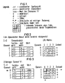
- Each element E i with i ⁇ ⁇ 0, ..., n-1 ⁇ is in a state Z at time t t i with Z t i ⁇ ⁇ undef, 0, ..., n-1 ⁇ , which contains information about the order of access to this element.
- Several elements can have the state "undef", which means that they are undefined, ie they are free. However, if they are defined, the state-element relationship is bijective, ie each state value can only be occupied by exactly one element.
- 2nd case element reassignment if undefined elements exist (e.g. reassign a free memory page):
- 3rd case element reassignment if all elements are defined; the one that has not been used for the longest time is overwritten (e.g. relocate the oldest ASP page and relocate this page):
- the method is implemented using a quadratic binary matrix of order n without a main diagonal.
- One line is assigned to each element.
- In each row of the Boolean matrix there is one column element, one bit for each element, except for the own element.
- n ⁇ IN is the number of elements.
- a power of two is often chosen for n.
- the elements When resetting, the elements must be marked as "undefined".
- the counter C is to be set to the value 0.
- the matrix elements are undefined, but can take any values.
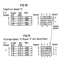
- the valid part of the binary matrix is antisymmetric in its value assignment with regard to its main diagonals. All permissible operations of the algorithm receive this antisymmetry.
- the binary matrix is increased by 1 with regard to the order (i.e. also in the rank of the matrix) of the matrix part used.
- each matrix cell can also be spatially assigned to an element and only has to be installed if the associated element is also installed.
- the circuit can of course also be modified in such a way that serial access is made. This may be desirable for larger applications.
- the circuit arrangement according to FIG. 12 contains an arrangement designed as a full matrix M with k rows and m columns, in which full matrix M at each intersection of a row with a column, with the exception of those intersections that fall into the main diagonal of the full matrix M, a crosspoint individual memory element FF is provided, all the memory elements FF having the same structure, and a control device S with a control logic CL , a counter C, a (1 out of n) decoder D, a multiplexer MUX and a comparator KOMP, the n elements on the input side being connected to a common address, request search term introduction or the like and an individual output line of the multiplexer MUX the n elements on the output side with a first input of a row-individual input link EZG, the output of which is connected to a respective row-specific matrix column set / deletion line and from which a second input together with all second inputs of all further row-individual inputs Angs logic elements EZG is connected to a matrix-
- the outputs of all storage element FF which are individual to the intersection point, one line of the full matrix M, are each connected to an input of a line-specific output logic element AZG, the outputs of which are individually connected to first inputs of the multiplexer MUX, which multiplexer MUX has individual second inputs output signals of ) Decoders D and control signals from the control logic CL are supplied via corresponding control field outputs on the element field via an enable input EN and a selection input SEL.
- a reset signal and a clock signal can be fed to the counter C from the control logic CL via corresponding inputs.
- the counter C outputs a binary-coded output signal 2 ⁇ , which is supplied to both the (1 out of n) decoder D and corresponding first inputs of the comparator Komp.
- the comparator Komp is binary coded Comparison signal 2 '' supplied.
- An output signal line of the comparator Komp is connected to a corresponding element field-side signal input of the control logic CL, wherein whenever the comparator outputs a predetermined comparison output signal, this acts at least indirectly on the selection input SEL through the control logic CL.
- the input link and the output link AZG are each preferably implemented as a NAND link.
- Each subfield T0 ... T n has on the one hand a first, input-side register SB, a memory element d, a second output-side register SB value, an output signal amplifier V, an input-side comparator KompE and a logic element G, the n elements on the input side an address line and a common set / clear line from the control logic CL are connected.
- the logic element G has an AND function.
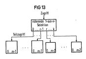
- the elements of each group are managed by the LRU mechanism. B. can be implemented as described above.
- the sketched binary matrix tree can also be created deeper for a specific solution.
- the advantage of this circuit is the fast, non-serial access to the LRU information.
- 1st case element access (e.g. read / write page in RAM):
- the search term fields of all elements must be searched "within" all groups.
- the element with a hit is the one you are looking for and provides the required information for a read access or records the date for a write access.
- the states are calculated normally (as described previously). Similarly, the states of the top matrix are newly formed. This is the deviation of the proposed method from the correct LRU mechanism.
- the top matrix indicates the group that has not been accessed for the longest time. Within the group, the member set of locally the oldest known. This is usually not the "oldest” of all elements. If the group containing the "oldest” element is accessed, the status in the top matrix for this group is set to the "youngest” value. Another system-wide "very old” element of the same group is only overwritten after small entries. In principle, the "oldest" element of the selected group is always overwritten when a new assignment is made.
- the top matrix control mechanism therefore does not implement the LRU mechanism for the overall structure, but is a solution for a stochastically reasonable distribution.
- 2nd case element reassignment if undefined elements exist (e.g. reassign a free memory page):
- the free elements are assigned in order. The easiest way to do this is with a counter.
- the allocation algorithm is freely selectable, but it depends on the application. It can be said that filling up from one group to another is generally very unfavorable. It is best to add one element to the groups in turn. This ensures that the group-oldest "oldest" entries are also the "oldest" of the overall system before the 3rd case comes into play.
- 3rd case element reassignment if all elements are defined (e.g. outsource an ASP page and relocate this page):
Landscapes
- Engineering & Computer Science (AREA)
- Theoretical Computer Science (AREA)
- Physics & Mathematics (AREA)
- General Engineering & Computer Science (AREA)
- General Physics & Mathematics (AREA)
- Memory System Of A Hierarchy Structure (AREA)
Applications Claiming Priority (2)
| Application Number | Priority Date | Filing Date | Title |
|---|---|---|---|
| DE3733044 | 1987-09-30 | ||
| DE3733044 | 1987-09-30 |
Publications (2)
| Publication Number | Publication Date |
|---|---|
| EP0309712A2 true EP0309712A2 (fr) | 1989-04-05 |
| EP0309712A3 EP0309712A3 (fr) | 1990-06-20 |
Family
ID=6337297
Family Applications (1)
| Application Number | Title | Priority Date | Filing Date |
|---|---|---|---|
| EP88113273A Withdrawn EP0309712A3 (fr) | 1987-09-30 | 1988-08-16 | Système de réalisation d'un mécanisme de type LRU (le moins récemment utilisé) pour plus de trois termes par des arbres de matrices binaires |
Country Status (1)
| Country | Link |
|---|---|
| EP (1) | EP0309712A3 (fr) |
Family Cites Families (4)
| Publication number | Priority date | Publication date | Assignee | Title |
|---|---|---|---|---|
| GB1161930A (en) * | 1967-07-11 | 1969-08-20 | Ibm | Indicating Circuit |
| GB1278220A (en) * | 1971-03-13 | 1972-06-21 | Ibm | Indicating circuit |
| JPS5226124A (en) * | 1975-08-22 | 1977-02-26 | Fujitsu Ltd | Buffer memory control unit |
| JPH0614325B2 (ja) * | 1984-02-02 | 1994-02-23 | 日本電気株式会社 | リプレ−スメント方式 |
-
1988
- 1988-08-16 EP EP88113273A patent/EP0309712A3/fr not_active Withdrawn
Also Published As
| Publication number | Publication date |
|---|---|
| EP0309712A3 (fr) | 1990-06-20 |
Similar Documents
| Publication | Publication Date | Title |
|---|---|---|
| DE2803989C2 (de) | Digitaldatenspeicher mit wahlfreiem Zugriff | |
| DE69218941T2 (de) | Neuronale netzwerk architektur | |
| DE4206286C2 (de) | Speicherzugriffssystem und Verfahren zum Ausgeben eines digitalen Datenstromes | |
| DE3327379A1 (de) | Einrichtung und verfahren zum umordnen von datensaetzen | |
| WO1996033499A1 (fr) | Memoire adressable par le contenu | |
| DE1901343A1 (de) | Datenverarbeitungsanlage mit mehreren Verarbeitungseinheiten und an diese angeschlossenen Speichereinheiten | |
| DE3015875A1 (de) | Speicherzugriffssystem und verfahren fuer einen zugriff zu einem digitalen speichersystem | |
| DE2331589A1 (de) | Datenverarbeitungsanordnung | |
| DE1774052B1 (de) | Rechner | |
| DE2423265C3 (de) | Optimierende Rechenmaschine | |
| DE3788617T2 (de) | Vektordatenverarbeitungssystem mit einer E/A-Steuerung für jeden Vektordatenprozessor und einer anderen E/A-Steuerung für mindestens einen anderen Vektordatenprozessor. | |
| DE2926322A1 (de) | Speicher-subsystem | |
| DE69025782T2 (de) | Registerbankschaltung | |
| DE69227144T2 (de) | Programmierbare logische Einheit | |
| DE10105627B4 (de) | Mehrfachanschlussspeichereinrichtung, Verfahren und System zum Betrieb einer Mehrfachanschlussspeichereinrichtung | |
| DE2403669B2 (de) | SpezialComputer | |
| DE2556357A1 (de) | Adressiereinrichtung | |
| DE2744886A1 (de) | Verfahren und geraet zum umschwenken einer binaerdatenmatrix, besonders zur anwendung als speicherelement mit zwei zugriffsmodi bei elektronenrechnern | |
| DE69206604T2 (de) | Schnelle Addierkette. | |
| EP0882294B1 (fr) | Memoire rom et procede de commande correspondant | |
| EP0309667B1 (fr) | Circuit pour systèmes de traitement de données réalisant un mécanisme de type LRU (Last Recently Used) organisé de façon modulaire, extensible, pour n éléments | |
| EP0309712A2 (fr) | Système de réalisation d'un mécanisme de type LRU (le moins récemment utilisé) pour plus de trois termes par des arbres de matrices binaires | |
| DE3149926A1 (de) | Programmierbare vergleichsschaltung | |
| EP0309737A2 (fr) | Système de réalisation d'un mécanisme de type LRU (le moins récemment utilisé) pour plus de trois termes par des arbres de matrices binaires | |
| DE69011623T2 (de) | Verfahren und Vorrichtung für Umschaltung von Dateninformation durch einen digitalen Wähler. |
Legal Events
| Date | Code | Title | Description |
|---|---|---|---|
| PUAI | Public reference made under article 153(3) epc to a published international application that has entered the european phase |
Free format text: ORIGINAL CODE: 0009012 |
|
| AK | Designated contracting states |
Kind code of ref document: A2 Designated state(s): AT BE CH DE FR GB IT LI LU NL SE |
|
| PUAL | Search report despatched |
Free format text: ORIGINAL CODE: 0009013 |
|
| AK | Designated contracting states |
Kind code of ref document: A3 Designated state(s): AT BE CH DE FR GB IT LI LU NL SE |
|
| STAA | Information on the status of an ep patent application or granted ep patent |
Free format text: STATUS: THE APPLICATION IS DEEMED TO BE WITHDRAWN |
|
| 18D | Application deemed to be withdrawn |
Effective date: 19901221 |