EP0309894A2 - Dispositif à semi-conducteur de puissance - Google Patents
Dispositif à semi-conducteur de puissance Download PDFInfo
- Publication number
- EP0309894A2 EP0309894A2 EP88115524A EP88115524A EP0309894A2 EP 0309894 A2 EP0309894 A2 EP 0309894A2 EP 88115524 A EP88115524 A EP 88115524A EP 88115524 A EP88115524 A EP 88115524A EP 0309894 A2 EP0309894 A2 EP 0309894A2
- Authority
- EP
- European Patent Office
- Prior art keywords
- semiconductor element
- power semiconductor
- contact
- insulator
- spring contacts
- Prior art date
- Legal status (The legal status is an assumption and is not a legal conclusion. Google has not performed a legal analysis and makes no representation as to the accuracy of the status listed.)
- Withdrawn
Links
Images
Classifications
-
- H—ELECTRICITY
- H10—SEMICONDUCTOR DEVICES; ELECTRIC SOLID-STATE DEVICES NOT OTHERWISE PROVIDED FOR
- H10W—GENERIC PACKAGES, INTERCONNECTIONS, CONNECTORS OR OTHER CONSTRUCTIONAL DETAILS OF DEVICES COVERED BY CLASS H10
- H10W76/00—Containers; Fillings or auxiliary members therefor; Seals
- H10W76/10—Containers or parts thereof
- H10W76/12—Containers or parts thereof characterised by their shape
- H10W76/13—Containers comprising a conductive base serving as an interconnection
- H10W76/138—Containers comprising a conductive base serving as an interconnection having another interconnection being formed by a cover plate parallel to the conductive base, e.g. sandwich type
-
- H—ELECTRICITY
- H10—SEMICONDUCTOR DEVICES; ELECTRIC SOLID-STATE DEVICES NOT OTHERWISE PROVIDED FOR
- H10W—GENERIC PACKAGES, INTERCONNECTIONS, CONNECTORS OR OTHER CONSTRUCTIONAL DETAILS OF DEVICES COVERED BY CLASS H10
- H10W72/00—Interconnections or connectors in packages
Definitions
- the invention relates to a power semiconductor element according to the preamble of claim 1.
- a multi-spring contact is a component that consists of a large number of resilient individual elements. These have the property of springing in three levels. Therefore, mechanical stresses no longer occur even after the individual elements have been soldered to the semiconductor crystal. It turns out, however, that the solder connections required for this purpose between the semiconductor wafer and the multi-spring contacts made very difficult soldering processes necessary, which make the component more expensive.
- the object of the invention is to improve a semiconductor element for greater performances in such a way that the same good properties as in the case of soldered multi-spring contacts are achieved while avoiding difficult soldering processes.
- a particularly advantageous embodiment is obtained when a bracing device (eyebolt) is supported on the annular insulator and the base plate and cover plate designed as contact blocks press against one another, as a result of which the multi-spring contacts are braced against the semiconductor crystal with a predeterminable compressive force.
- the contact pressure is generated within the closed semiconductor housing, the clamping force extending from the clamping device (eye bolt) via the upper contact block, the upper multi-spring contact, the semiconductor crystal, the lower multi-spring contact, the lower contact block and the annular insulator to the clamping device.
- the pressing of the multi-spring contacts onto the semiconductor wafer results in the same good electrical and thermal contacts as when soldering. Furthermore, it has been shown that, because of the large number of contact points of the multi-spring contacts, only half the contact force is required, as in the case of conventional pressure contacting. If the contact force of the selected semiconductor element is approximately 20 kN, since only half the contact force is required for the multi-spring contact, the contact force during production must be set to 11 kN at 20 ° C. At minus 50 ° C there would still be sufficient contact pressure and at 150 ° C 30 kN would occur. This corresponds to a value that is still 35% smaller than the contact force to be set for the pressure contact. In reality, the force difference is less than 3 kN, as well the tendons are heated and stretch, which results in minor changes in length at the multi-spring contacts.
- the annular insulator should have an L-shaped cross section, the smaller leg being directed radially inwards and the larger leg being axially directed.
- each contact block has different diameters in height, the diameter of the outward-facing contact block side being slightly smaller than the inside diameter formed by the small leg of the L-shaped insulator, and a collar for storage on the side of the contact blocks facing the interior of the semiconductor element is provided on an abutment of the L-shaped insulator or the tensioning device.
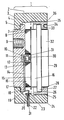
- the multi-spring contacts 16 consist of a multiplicity of spring elements 8.
- the lower multi-spring contact is provided with a central bore 13, into which an axially resilient sleeve is provided 12 is inserted.
- the spring elements 8 are held together by an outer, also axially resilient bushing 7.
- a lower contact block 17 and an upper contact block 32 are in galvanic connection with the multi-spring contacts 16, which can be cohesive or non-positive.
- the lower contact block 17 has a collar 18, an inner bore 11 and at least one outer threaded bore 9 for the anode connection and for a non-positive thermal connection.
- the upper contact block 32 is provided with a collar 27.
- a slot 14 is present in at least one of the contact blocks - preferably in the lower contact block 17.
- the lower and upper multi-spring contacts 16 are separated by an annular insulator 24, e.g. made of ceramic, which can be provided with ribs, not shown, for extending the external creeping path, and clamped an eyebolt 33.
- the annular part 2 of the insulator 24 has an inwardly extending collar in its lower part and an internal thread 36 at the top.
- the cross section of the annular part 2 is L-shaped, the longer leg being axially directed and the shorter leg in the lower part points radially inwards.
- the eyebolt 33 engages in the internal thread 36.
- the collar 28 of the eyebolt 33 forms the abutment to the collar 27 of the upper contact block 32.
- the eyebolt 33 is provided with at least two outwardly directed bores 34 in which a screwing tool can be attached.
- a small pressure contact 31 in the form of a spiral spring 30 is provided for the galvanic contacting of the gate of the semiconductor crystal 15.
- the coil spring 30 is connected to an electrical line 23.
- the coil spring 30 is electrically insulated by an insulating potty 10 inserted into the inner bore 11 of the lower contact block 17 and the electrical line 23 inserted into the slot 14 by an insulating tube 19.
- the end 22 of the electrical line 23 is soldered into a tube 21.
- the tube 21 inserted in the insulator 24 is part of a pump and electrical connector device 20 (not shown further) for the external gate connection.
- the cathode connection to be guided over the upper contact block 32 is not shown.
- the semiconductor element is assembled and contacted as described below:
- the lower contact block 17 is inserted inside the insulator 24.
- the pressure contact 31 is inserted into the provided inner bore 11 and the line end 22 of the electrical line 23 is inserted into the tube 21 and soldered to it.
- the lower multi-spring contact 16 can also be integrally connected to the lower contact block 17 by soldering. Then the line 23 must be threaded into the slot 14.
- the semiconductor crystal 15 is then placed on the lower multi-spring contact 16 and centered by an insulator, not shown, for example made of plastic. Then the upper multi-spring contact 16 and the upper contact block 32 are placed. These two components can be centered with one another by a material connection (soldering). The eyebolt 33 is now screwed in by hand until its collar 28 on the collar 27 of the upper contact block 32 rests. The upper contact block 32 and the associated upper multi-contact 16 are thus centered.
- the semiconductor element 1 is brought under a press with a force display.
- the semiconductor element rests on the end face 3 of the insulator 24 and the compressive force is introduced via the end face 29 of the upper contact block 32.
- the contact force is slowly increased by tightening the eyebolt until its value is slightly higher than the nominal force.
- the "atmosphere" of the interior 3 of the semiconductor element 1 must be and remain clean and dry. Between the contact blocks 17, 32 and the insulator 24, respectively. the eyebolt 33 and between the thread 35 and the insulator 24 should therefore be gastight. The best way to do this is on the supports of frets 18, 27, 28, for which there are several options.
- a permanently elastic sealing compound 5 or 26 can be used, which also absorbs the thermal relative movements.
- the eyebolt 33 made of appropriate steel, for example Invar steel, is provided with an adhesive 25 on the thread 35, 36 before it is screwed in, which sets with a time delay and thus seals on this actuator.
- bracing takes place via the insulator 24.
- gas tightness can also be produced in a different way. For example, thermal compression welding on the frets 18, 27, 28 with the interposition of a thin aluminum disc would be conceivable.
- the multi-spring contacts 16 can consist of a multiplicity of spring struts which arise when, in the case of a metal strip which has been stamped in a multiple arrow shape, the connecting webs are removed on one side on the side facing the semiconductor crystal after the spiral winding.
- the multi-spring contacts 16 can also consist of a multiplicity of individual wires which are twisted in the axial direction.
Landscapes
- Die Bonding (AREA)
Applications Claiming Priority (4)
| Application Number | Priority Date | Filing Date | Title |
|---|---|---|---|
| DE3732584 | 1987-09-28 | ||
| DE3732584 | 1987-09-28 | ||
| DE3826820 | 1988-08-06 | ||
| DE19883826820 DE3826820A1 (de) | 1987-09-28 | 1988-08-06 | Leistungshalbleiterelement |
Publications (2)
| Publication Number | Publication Date |
|---|---|
| EP0309894A2 true EP0309894A2 (fr) | 1989-04-05 |
| EP0309894A3 EP0309894A3 (fr) | 1990-09-26 |
Family
ID=25860213
Family Applications (1)
| Application Number | Title | Priority Date | Filing Date |
|---|---|---|---|
| EP19880115524 Withdrawn EP0309894A3 (fr) | 1987-09-28 | 1988-09-22 | Dispositif à semi-conducteur de puissance |
Country Status (4)
| Country | Link |
|---|---|
| EP (1) | EP0309894A3 (fr) |
| JP (1) | JPH01128437A (fr) |
| CN (1) | CN1032471A (fr) |
| DE (1) | DE3826820A1 (fr) |
Cited By (3)
| Publication number | Priority date | Publication date | Assignee | Title |
|---|---|---|---|---|
| EP1791178A3 (fr) * | 2005-11-23 | 2011-02-23 | Semikron Elektronik GmbH & Co. KG Patentabteilung | Module de puissance semi-conducteur de type à contact par pression |
| CN103579165A (zh) * | 2013-11-04 | 2014-02-12 | 国家电网公司 | 一种全压接式功率器件 |
| CN105895452A (zh) * | 2016-05-27 | 2016-08-24 | 浙江英洛华新能源科技有限公司 | 密封型高压直流继电器 |
Families Citing this family (4)
| Publication number | Priority date | Publication date | Assignee | Title |
|---|---|---|---|---|
| JP2502386B2 (ja) * | 1989-04-11 | 1996-05-29 | 富士電機株式会社 | 半導体装置 |
| DE102006034964B3 (de) * | 2006-07-28 | 2007-09-06 | Semikron Elektronik Gmbh & Co. Kg | Anordnung mit einem Leistungshalbleiterbauelement und mit einer Kontakteinrichtung |
| CN102082132B (zh) * | 2010-11-03 | 2015-11-11 | 北京航天万方科技有限公司 | 一种大功率半导体模块 |
| CN104362141B (zh) * | 2014-11-26 | 2017-06-23 | 国家电网公司 | 一种大功率压接型igbt模块 |
Family Cites Families (7)
| Publication number | Priority date | Publication date | Assignee | Title |
|---|---|---|---|---|
| DE2855493A1 (de) * | 1978-12-22 | 1980-07-03 | Bbc Brown Boveri & Cie | Leistungs-halbleiterbauelement |
| DE2942401C2 (de) * | 1979-10-19 | 1984-09-06 | Siemens AG, 1000 Berlin und 8000 München | Halbleiterbauelement mit mehreren Halbleiterkörpern |
| DE3308720A1 (de) * | 1983-03-11 | 1984-09-13 | Siemens AG, 1000 Berlin und 8000 München | Halbleiterbauelement mit scheibenfoermigem gehaeuse |
| JPS60150670A (ja) * | 1984-01-17 | 1985-08-08 | Mitsubishi Electric Corp | 半導体装置 |
| JPS61134067A (ja) * | 1984-12-05 | 1986-06-21 | Fuji Electric Co Ltd | 半導体装置 |
| JPS61208873A (ja) * | 1985-03-13 | 1986-09-17 | Res Dev Corp Of Japan | 圧接構造型両面ゲ−ト静電誘導サイリスタ |
| US4829364A (en) * | 1985-11-29 | 1989-05-09 | Mitsubishi Denki Kabushiki Kaisha | Semiconductor device |
-
1988
- 1988-08-06 DE DE19883826820 patent/DE3826820A1/de not_active Withdrawn
- 1988-09-22 EP EP19880115524 patent/EP0309894A3/fr not_active Withdrawn
- 1988-09-27 CN CN88109038A patent/CN1032471A/zh active Pending
- 1988-09-28 JP JP63243736A patent/JPH01128437A/ja active Pending
Cited By (4)
| Publication number | Priority date | Publication date | Assignee | Title |
|---|---|---|---|---|
| EP1791178A3 (fr) * | 2005-11-23 | 2011-02-23 | Semikron Elektronik GmbH & Co. KG Patentabteilung | Module de puissance semi-conducteur de type à contact par pression |
| CN103579165A (zh) * | 2013-11-04 | 2014-02-12 | 国家电网公司 | 一种全压接式功率器件 |
| CN103579165B (zh) * | 2013-11-04 | 2016-08-31 | 国家电网公司 | 一种全压接式功率器件 |
| CN105895452A (zh) * | 2016-05-27 | 2016-08-24 | 浙江英洛华新能源科技有限公司 | 密封型高压直流继电器 |
Also Published As
| Publication number | Publication date |
|---|---|
| DE3826820A1 (de) | 1989-04-06 |
| EP0309894A3 (fr) | 1990-09-26 |
| CN1032471A (zh) | 1989-04-19 |
| JPH01128437A (ja) | 1989-05-22 |
Similar Documents
| Publication | Publication Date | Title |
|---|---|---|
| DE2434627C3 (de) | Kühlvorrichtung für ein integriertes Halbleiterbauelement | |
| EP2548265B1 (fr) | Connecteur pour courants elevés | |
| DE3722069C2 (fr) | ||
| DE3031802C2 (fr) | ||
| DE7118954U (de) | Schleifring-Satz für umlaufende elektrische Maschinen | |
| WO2004077587A2 (fr) | Production d'un empilement de piles a combustible haute temperature | |
| EP3208837B1 (fr) | Module électrique comprenant un composant électrique | |
| EP0309894A2 (fr) | Dispositif à semi-conducteur de puissance | |
| DE3520855C1 (de) | Galvanische Zelle mit Presskontaktierung | |
| EP0597147B1 (fr) | Installation blindée à haute tension et assemblage pour une telle installation | |
| WO2018083295A1 (fr) | Système de ligne électrique blindé et boîtier de blindage | |
| EP0124705A1 (fr) | Dispositif semi-conducteur ayant une plaquette semi-conductrice et un corps isolant en forme d'anneau | |
| DE69934559T2 (de) | Einbau des Einschaltwiderstandes für Hochspannungsanlage | |
| DE2611161C2 (fr) | ||
| DE3623399C1 (en) | Totally insulated anchor clamp (tension clamp, dead-end clamp) | |
| DE2238755A1 (de) | Ankerblechpaket fuer eine elektrische maschine | |
| DE29815396U1 (de) | Anschlußvorrichtung | |
| DE102017219434B4 (de) | Aktuatorbaugruppe, damit ausgestatteter Membran-Polymeraktuator und Herstellungsverfahren | |
| EP0210126B1 (fr) | Pièce de contact d'accouplement pour un enfichage entre deux conducteurs cylindriques d'une installation de commutation haute tension à isolation sous pression gazeuse en enceinte fermée | |
| EP0139882B1 (fr) | Connexion entre les extrémités des enroulements d'induit et des segments relatifs du collecteur | |
| DE2109119A1 (de) | Nietdichtungsvorrichtung | |
| DE3127284A1 (de) | Batterieklemme | |
| DE2927860A1 (de) | Vorrichtung zum einspannen eines scheibenfoermigen halbleiterbauelements zwischen zwei kuehlkoerper | |
| EP0931326B1 (fr) | Procede de fabrication d'un condensateur a faible inductance propre | |
| DE813560C (de) | Isolierte Durchfuehrung |
Legal Events
| Date | Code | Title | Description |
|---|---|---|---|
| PUAI | Public reference made under article 153(3) epc to a published international application that has entered the european phase |
Free format text: ORIGINAL CODE: 0009012 |
|
| AK | Designated contracting states |
Kind code of ref document: A2 Designated state(s): CH DE FR GB IT LI NL SE |
|
| PUAL | Search report despatched |
Free format text: ORIGINAL CODE: 0009013 |
|
| AK | Designated contracting states |
Kind code of ref document: A3 Designated state(s): CH DE FR GB IT LI NL SE |
|
| STAA | Information on the status of an ep patent application or granted ep patent |
Free format text: STATUS: THE APPLICATION IS DEEMED TO BE WITHDRAWN |
|
| 18D | Application deemed to be withdrawn |
Effective date: 19910226 |