EP0310353A2 - Détecteur à couches minces à gain élevé - Google Patents
Détecteur à couches minces à gain élevé Download PDFInfo
- Publication number
- EP0310353A2 EP0310353A2 EP88308983A EP88308983A EP0310353A2 EP 0310353 A2 EP0310353 A2 EP 0310353A2 EP 88308983 A EP88308983 A EP 88308983A EP 88308983 A EP88308983 A EP 88308983A EP 0310353 A2 EP0310353 A2 EP 0310353A2
- Authority
- EP
- European Patent Office
- Prior art keywords
- layer
- thin film
- film sensor
- sensor
- semiconductor layers
- Prior art date
- Legal status (The legal status is an assumption and is not a legal conclusion. Google has not performed a legal analysis and makes no representation as to the accuracy of the status listed.)
- Withdrawn
Links
- 239000010409 thin film Substances 0.000 title claims abstract description 21
- 239000004065 semiconductor Substances 0.000 claims abstract description 28
- 230000004888 barrier function Effects 0.000 claims description 29
- 229910021417 amorphous silicon Inorganic materials 0.000 claims description 21
- 229910000577 Silicon-germanium Inorganic materials 0.000 claims description 2
- 230000001747 exhibiting effect Effects 0.000 claims 1
- 230000000903 blocking effect Effects 0.000 abstract description 8
- 239000010410 layer Substances 0.000 description 77
- 230000035945 sensitivity Effects 0.000 description 12
- 239000000463 material Substances 0.000 description 10
- 230000003287 optical effect Effects 0.000 description 7
- 239000000758 substrate Substances 0.000 description 7
- 230000000694 effects Effects 0.000 description 4
- 239000011521 glass Substances 0.000 description 4
- 230000004044 response Effects 0.000 description 4
- BLRPTPMANUNPDV-UHFFFAOYSA-N Silane Chemical compound [SiH4] BLRPTPMANUNPDV-UHFFFAOYSA-N 0.000 description 3
- 238000013459 approach Methods 0.000 description 3
- 239000002800 charge carrier Substances 0.000 description 3
- 238000005094 computer simulation Methods 0.000 description 3
- 238000000354 decomposition reaction Methods 0.000 description 3
- 230000009977 dual effect Effects 0.000 description 3
- 238000000034 method Methods 0.000 description 3
- 238000005215 recombination Methods 0.000 description 3
- 230000006798 recombination Effects 0.000 description 3
- 229910000077 silane Inorganic materials 0.000 description 3
- ZOXJGFHDIHLPTG-UHFFFAOYSA-N Boron Chemical compound [B] ZOXJGFHDIHLPTG-UHFFFAOYSA-N 0.000 description 2
- VYZAMTAEIAYCRO-UHFFFAOYSA-N Chromium Chemical compound [Cr] VYZAMTAEIAYCRO-UHFFFAOYSA-N 0.000 description 2
- XYFCBTPGUUZFHI-UHFFFAOYSA-N Phosphine Chemical compound P XYFCBTPGUUZFHI-UHFFFAOYSA-N 0.000 description 2
- 229910045601 alloy Inorganic materials 0.000 description 2
- 239000000956 alloy Substances 0.000 description 2
- 229910052782 aluminium Inorganic materials 0.000 description 2
- XAGFODPZIPBFFR-UHFFFAOYSA-N aluminium Chemical compound [Al] XAGFODPZIPBFFR-UHFFFAOYSA-N 0.000 description 2
- 230000015572 biosynthetic process Effects 0.000 description 2
- 229910052796 boron Inorganic materials 0.000 description 2
- 230000015556 catabolic process Effects 0.000 description 2
- 229910052804 chromium Inorganic materials 0.000 description 2
- 239000011651 chromium Substances 0.000 description 2
- 230000008878 coupling Effects 0.000 description 2
- 238000010168 coupling process Methods 0.000 description 2
- 238000005859 coupling reaction Methods 0.000 description 2
- 238000004519 manufacturing process Methods 0.000 description 2
- 238000000623 plasma-assisted chemical vapour deposition Methods 0.000 description 2
- 230000009467 reduction Effects 0.000 description 2
- XUIMIQQOPSSXEZ-UHFFFAOYSA-N Silicon Chemical compound [Si] XUIMIQQOPSSXEZ-UHFFFAOYSA-N 0.000 description 1
- 238000010276 construction Methods 0.000 description 1
- 230000007547 defect Effects 0.000 description 1
- 230000002950 deficient Effects 0.000 description 1
- 238000000151 deposition Methods 0.000 description 1
- 230000008021 deposition Effects 0.000 description 1
- 230000005684 electric field Effects 0.000 description 1
- AMGQUBHHOARCQH-UHFFFAOYSA-N indium;oxotin Chemical compound [In].[Sn]=O AMGQUBHHOARCQH-UHFFFAOYSA-N 0.000 description 1
- 230000000873 masking effect Effects 0.000 description 1
- 229910021424 microcrystalline silicon Inorganic materials 0.000 description 1
- 229910000073 phosphorus hydride Inorganic materials 0.000 description 1
- 229910021420 polycrystalline silicon Inorganic materials 0.000 description 1
- 238000005036 potential barrier Methods 0.000 description 1
- 238000009877 rendering Methods 0.000 description 1
- 230000000630 rising effect Effects 0.000 description 1
- 229910052710 silicon Inorganic materials 0.000 description 1
- 239000010703 silicon Substances 0.000 description 1
- 239000002356 single layer Substances 0.000 description 1
- 230000001629 suppression Effects 0.000 description 1
Images


Classifications
-
- H—ELECTRICITY
- H10—SEMICONDUCTOR DEVICES; ELECTRIC SOLID-STATE DEVICES NOT OTHERWISE PROVIDED FOR
- H10F—INORGANIC SEMICONDUCTOR DEVICES SENSITIVE TO INFRARED RADIATION, LIGHT, ELECTROMAGNETIC RADIATION OF SHORTER WAVELENGTH OR CORPUSCULAR RADIATION
- H10F19/00—Integrated devices, or assemblies of multiple devices, comprising at least one photovoltaic cell covered by group H10F10/00, e.g. photovoltaic modules
- H10F19/50—Integrated devices comprising at least one photovoltaic cell and other types of semiconductor or solid-state components
-
- H—ELECTRICITY
- H10—SEMICONDUCTOR DEVICES; ELECTRIC SOLID-STATE DEVICES NOT OTHERWISE PROVIDED FOR
- H10F—INORGANIC SEMICONDUCTOR DEVICES SENSITIVE TO INFRARED RADIATION, LIGHT, ELECTROMAGNETIC RADIATION OF SHORTER WAVELENGTH OR CORPUSCULAR RADIATION
- H10F30/00—Individual radiation-sensitive semiconductor devices in which radiation controls the flow of current through the devices, e.g. photodetectors
- H10F30/20—Individual radiation-sensitive semiconductor devices in which radiation controls the flow of current through the devices, e.g. photodetectors the devices having potential barriers, e.g. phototransistors
- H10F30/21—Individual radiation-sensitive semiconductor devices in which radiation controls the flow of current through the devices, e.g. photodetectors the devices having potential barriers, e.g. phototransistors the devices being sensitive to infrared, visible or ultraviolet radiation
- H10F30/24—Individual radiation-sensitive semiconductor devices in which radiation controls the flow of current through the devices, e.g. photodetectors the devices having potential barriers, e.g. phototransistors the devices being sensitive to infrared, visible or ultraviolet radiation the devices having only two potential barriers, e.g. bipolar phototransistors
- H10F30/245—Bipolar phototransistors
-
- H—ELECTRICITY
- H10—SEMICONDUCTOR DEVICES; ELECTRIC SOLID-STATE DEVICES NOT OTHERWISE PROVIDED FOR
- H10F—INORGANIC SEMICONDUCTOR DEVICES SENSITIVE TO INFRARED RADIATION, LIGHT, ELECTROMAGNETIC RADIATION OF SHORTER WAVELENGTH OR CORPUSCULAR RADIATION
- H10F77/00—Constructional details of devices covered by this subclass
- H10F77/10—Semiconductor bodies
- H10F77/16—Material structures, e.g. crystalline structures, film structures or crystal plane orientations
- H10F77/169—Thin semiconductor films on metallic or insulating substrates
- H10F77/1692—Thin semiconductor films on metallic or insulating substrates the films including only Group IV materials
Definitions
- This invention relates to a multilayer thin film sensor comprising a pair of injecting contact semiconductor layers sandwiching plural intrinsic semiconductor layers.
- Thin film semiconductor materials have recently become viable materials for use in low cost, large area electronic applications. Their attractive electronic characteristics, coupled with the relative simplicity of their fabrication techniques enable the formation of active and passive devices as well as bus and address lines on a single, page size and larger, substrate. Materials such as amorphous silicon, polycrystalline silicon, microcrystalline silicon, and alloys of all these materials are now being used in these applications. While the present invention will be described with reference to amorphous silicon, it should be understood that other thin film semiconductor materials may be used with similar, if somewhat different, results.
- Photodetectors there are two main classes of photodetectors.
- Primary photocurrent devices i.e., photovoltaic devices, such as p-i-n solar cells, whose output current is limited to that which is internally generated, can achieve no more than unity optical gain, exhibit high light-to-dark sensitivity, and have fast response times (on the order of less than 1 microsecond for amorphous silicon).
- secondary photocurrent devices i.e., photoconductive devices, such as n-i-n diodes, whose output current is light enhanced and is a multiple of that which is internally generated, can achieve a high optical gain, although they exhibit low light-to-dark sensitivity and slow response times (on the order of milliseconds).
- a more useful sensor should have the high gain associated with photoconductive devices and the high light-to-dark sensitivity and fast response time associated with photovoltaic devices.
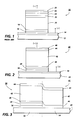
- the device reported therein is illustrated in Figure 1, and will be referred to herein as the Chang phototransistor 10. It is a multilayer structure made on an insulating glass substrate 12 over which there is an ITO (indium tin oxide) conductive layer 14, and includes a collector comprising an n+ layer 16, and n layer 18, a thick intrinsic semiconductor layer 20, a heavily doped (p+) base layer 22, a thin intrinsic semiconductor layer 24, and a n+ emitter layer 26 over which there is an aluminum contact layer 28.
- the emitter is negatively biased with respect to the collector so that a forward bias is established across the emitter-intrinsic-base portion (26-24-22) and a reverse bias is established across the base-intrinsic-collector portion (22-20-18/16).
- the Chang phototransistor has been duplicated and it has been observed both experimentally and by computer simulation that no gain is achieved in that device except at very high applied voltage values, relative to device thickness, where the electrical field is close to breakdown. Furthermore, at these very high negative voltage levels the optical gain is small and the light-to-dark sensitivity is extremely poor, so that any sensor applications are impractical.
- a multilayer thin film sensor comprising a pair of injecting contact semiconductor layers sandwiching plural intrinsic semiconductor layers characterised by barrier means means therein for suppressing dark current flow and allowing high current flow so that said sensor exhibits a photoelectric gain greater than 3 and a corresponding light-to-dark ratio greater than 30 to 1.
- the injecting contacts sandwich a bulk of intrinsic amorphous thin film semiconductor within which there is one or more barrier layers whose purpose is to suppress dark current while having very little or no effect on light current, thereby allowing the gain and the light-to-dark sensitivity to be high.
- a lightly doped p-type semiconductor layer is located between intrinsic semiconductor layers of different thicknesses so that when the thin n-i-p portion is reverse biased and the thick n-i-p portion is forward biased a photoelectric gain greater than 3 and a corresponding light-to-dark ratio of greater than 30 to 1 is exhibited.
- the sensor device of the present invention to which the name "photoconductive diode (PCD)" has been applied, is illustrated in Figure 2. It comprises a multilayer structure 30 formed upon a glass substrate 32 overcoated with a conductive ohmic contact layer 34, such as aluminum or chromium.
- a typical amorphous silicon thin film PCD device 30 includes an n+ emitter layer 36, a thin intrinsic amorphous silicon layer 38, a p-type (lightly doped) base layer 40, a thick intrinsic amorphous silicon layer 42, and an n+ collector layer 44.
- a transparent, conductive, anti-reflection top layer 46 preferably of ITO
- the emitter 36 is positively biased with respect to the collector 44 so that a reverse bias is established across the emitter-intrinsic-base (36-38-40) portion and a forward bias is established across the base-intrinsic-collector (40-42-44) portion.
- the sensor of the present invention may be made of other suitable semiconductor materials.
- the PCD 30 is formed side-by-side, upon a single substrate 48 with a p-i-n+ solar cell 50, having substantially unity gain, as illustrated in Figure 3.
- Fabrication of this dual sample is extremely simple since it merely requires the masking of the substrate into two regions, namely, a sensor region 52 and a solar cell region 54, and the independent sequential deposition of the n+ emitter layer 36 and the thin intrinsic layer 38 only on the sensor region 52. Then the p-type base layer 40, the thick intrinsic layer 42 and the n+ collector layer 44 are deposited over both regions 52 and 54.
- a suitable fixture such as a black box
- Curve A represents a sample p-i-n solar cell illuminated with a light source of about 1015 photons/cm2-sec and curve B represents the solar cell in the dark. It is well known that the solar cell exhibits approximately unity gain under reverse bias, i.e., when the device is connected to an external bias circuit with the p layer being negative with respect to the n+ layer.
- the generally horizontal portion of curve A (at a current somewhat greater that 10 ⁇ 8 amp) provides a benchmark of unity gain.
- Curve B represents a sample PCD sensor, of the present invention, illuminated by the same light source and curve D represents the PCD in the dark. It can be seen that in a reverse bias condition, i.e., when the n+ emitter layer 36 is made negative relative to the n+ collector layer 44, only approximately unity gain is achieved.
- the I-V characteristics of a side-by-side Chang phototransistor and a p-i-n solar cell are compared in Figure 5.
- the n+ emitter and collector layers and both the thin and the thick intrinsic layers were made the same thickness as in the PCD. Only the base layers were different.
- the lightly doped PCD base layer (p) was 20 nm (200 ⁇ ) thick and was doped with 1000 ppm boron whereas the heavily doped Chang phototransistor base layer (p+) was 10 nm (100 ⁇ ) thick and was doped with forty times the boron, i.e. 40,000 ppm, in accordance with the teachings of the Chang et al article. It was determined that because of the very heavy doping of the p+ base layer, the operating characteristics of the Chang phototransistor would suffer unduly if the layer were made 10 nm (100 ⁇ ) thick as taught by Chang.
- Curves A′ and B′ again represent p-i-n solar cell characteristics substantially identical to the solar cell of Figure 4. Output differences are attributable to the differences in the base layer.
- the Chang phototransistor's operating characteristics are plotted in curves E (light) and F (dark). When illuminated, by the same light source as above, the phototransistor never exhibits a gain above unity either under forward or reverse bias.
- the benchmark for unity gain is the horizontal current output level of the reverse biased p-i-n solar cell (curve A′).
- the n+ emitter layer (26) is made positive with respect to the collector layer (16, 18)
- current through the sensor rises both in the light and in the dark. It should be noted that the dark current rises at a faster rate. Therefore, it can be concluded that when a significant gain level is achieved, this sensor would exhibit no useful light-to-dark sensitivity.
- p-i-n solar cells provide only primary photocurrent, meaning that the total current output is due solely to the light absorbed by the photosensitive material. In other words, one photon impinging upon the material will produce one electron and one hole and each will flow to its respective electrode, at which time the current ceases to flow, since the electrodes are blocking.
- photoconductive gain is obtained primarily from secondary photocurrent, meaning that current flows through the device and its external circuit many times, with the number of transits of the conducting carrier across the device defined as its gain.
- the Chang phototransistor incorporates a heavily doped p+ base layer to establish a high internal barrier, and the emitter is made more negative than the collector. Such a normal operating mode forward biases the emitter/thin intrinsic/base p+-i-n portion of the device, so as to reduce that internal barrier, and reverse biases the collector/thick intrinsic/base p+-i-n portion, so as to increase that internal barrier. Electron lifetime in a heavily doped p+ layer is very short because the p+ layer is very defective and the electrons cannot cross it easily without recombining. Therefore, both dark current and light current are suppressed (as illustrated in Figures 5 and 6), rendering the Chang phototransistor impractical as a sensor.
- the PCD base layer is lightly doped, and the emitter is made more positive than the collector.
- This normal operating mode reverse biases the emitter/thin intrinsic/base p-i-n portion of the device and forward biases the collector/thick intrinsic/base p- i-n portion. It is well known that under reverse bias the photovoltaic mode of photocurrent is expected, while under forward bias, the photoconductive mode is prevalent. Thus, in the PCD under normal operating conditions, photoconductive current flow is enhanced through its collector/thick intrinsic/base p-i-n portion, while simultaneously there is less opportunity for carrier losses by recombination in the lightly doped p layer.
- the PCD thin film sensor has been made by the standard PECVD (plasma enhanced chemical vapor deposition) method by which doped and undoped device grade amorphous silicon layers may be deposited.
- a glass substrate was provided as the support for a conductive layer of chromium, upon which was deposited sequentially: a 10nm to 50 nm layer of n+-type amorphous silicon by the decomposition of 99% silane and 1% phosphine (10,000ppm); a 30 nm layer of intrinsic amorphous silicon, formed from the decomposition of silane; a 20 nm layer of lightly doped, p-type amorphous silicon, formed from the decomposition of silane and 0.1% diborane (1000ppm); a 100 nm to 1 micron layer of intrinsic amorphous silicon; another 10 nm of n+ amorphous silicon; and, finally, a conductive transparent layer of ITO, for optically coupling the silicon to the air.
- PECVD
- the barrier can be adjusted by increasing the doping or increasing the thickness of the p-type layer.
- the effect of these increases is to introduce defects which hinder electron transport. Therefore, when providing the barrier, a balance must be struck between the desired formation of a potential barrier to the dark current and the undesired reduction of optical gain.
- multiple blocking layers could be employed and that this approach is more efficient that just using one internal blocking layer. For example, two blocking layers of a given thickness placed within the PCD, but spatially separated, are more effective at suppressing the dark current than one layer of double their thickness, while still preserving optical gain. This approach can be extended further so that three or more blocking layers may be used to improve the light to dark sensitivity of the sensor.
- a sensor having two blocking layers was modelled. It had the following configuration: a 10 nm n+ amorphous silicon layer; a 30 nm intrinsic amorphous silicon layer; a 10 nm p layer; a 400 nm intrinsic amorphous silicon layer; another 10 nm p layer, a 100 nm intrinsic amorphous silicon layer; and 10 nm n+ amorphous silicon layer.
- the thick intrinsic region of 500 nm was split into two regions with two p-type barrier layers (cumulatively 20 nm).
- the effect of the barrier in terms of dark current suppression, was that of a single layer 40 nm thick. But since there is less p material in the path of the charge carriers to cause recombination losses, there is less effect on the device gain.
- the barrier layer may be doped or undoped wide or narrow band gap alloys such as photoconductive SiC, SiN or SiGe forming a heterojuntion barrier layer, and may be polycrystalline or microcrystalline. Other changes in details of construction and in materials used may be resorted to
Landscapes
- Light Receiving Elements (AREA)
- Photometry And Measurement Of Optical Pulse Characteristics (AREA)
Applications Claiming Priority (2)
| Application Number | Priority Date | Filing Date | Title |
|---|---|---|---|
| US10207787A | 1987-09-29 | 1987-09-29 | |
| US102077 | 1987-09-29 |
Publications (2)
| Publication Number | Publication Date |
|---|---|
| EP0310353A2 true EP0310353A2 (fr) | 1989-04-05 |
| EP0310353A3 EP0310353A3 (fr) | 1989-08-16 |
Family
ID=22288014
Family Applications (1)
| Application Number | Title | Priority Date | Filing Date |
|---|---|---|---|
| EP88308983A Withdrawn EP0310353A3 (fr) | 1987-09-29 | 1988-09-28 | Détecteur à couches minces à gain élevé |
Country Status (2)
| Country | Link |
|---|---|
| EP (1) | EP0310353A3 (fr) |
| JP (1) | JPH01121724A (fr) |
Cited By (3)
| Publication number | Priority date | Publication date | Assignee | Title |
|---|---|---|---|---|
| US5554877A (en) * | 1988-05-06 | 1996-09-10 | Sharp Kabushiki Kaisha | Compound semiconductor electroluminescent device |
| US5705828A (en) * | 1991-08-10 | 1998-01-06 | Sanyo Electric Co., Ltd. | Photovoltaic device |
| US5872016A (en) * | 1996-06-18 | 1999-02-16 | Lucent Technologies Inc. | Process of making an optoelectronic devices utilizing multiple quantum well pin structures |
Families Citing this family (1)
| Publication number | Priority date | Publication date | Assignee | Title |
|---|---|---|---|---|
| JP4852936B2 (ja) * | 2005-08-31 | 2012-01-11 | アイシン精機株式会社 | 自動変速機の油圧制御装置 |
-
1988
- 1988-09-21 JP JP63237457A patent/JPH01121724A/ja active Pending
- 1988-09-28 EP EP88308983A patent/EP0310353A3/fr not_active Withdrawn
Non-Patent Citations (3)
| Title |
|---|
| IEEE ELECTRON DEVICE LETTERS, vol. EDL-8, no. 2, February 1987, pages 64-65, New York, US; K.C. CHANG et al.: "The amorphous Si/SiC heterojunction color-sensitive phototransistor" * |
| IEEE TRANSACTIONS ON ELECTRON DEVICES, vol. ED-32, no. 11, November 1985, pages 2192-2196, New York, US; B.S. WU et al.: "Amorphous silicon phototransistor on a glass substrate" * |
| IEEE TRANSACTIONS ON ELECTRON DEVICES, vol. ED-33, no. 11, November 1986, pages 1829-1830, New York, US; C.Y. CHANG: "Photogeneration and recombination in a bulk barrier phototransistor" * |
Cited By (3)
| Publication number | Priority date | Publication date | Assignee | Title |
|---|---|---|---|---|
| US5554877A (en) * | 1988-05-06 | 1996-09-10 | Sharp Kabushiki Kaisha | Compound semiconductor electroluminescent device |
| US5705828A (en) * | 1991-08-10 | 1998-01-06 | Sanyo Electric Co., Ltd. | Photovoltaic device |
| US5872016A (en) * | 1996-06-18 | 1999-02-16 | Lucent Technologies Inc. | Process of making an optoelectronic devices utilizing multiple quantum well pin structures |
Also Published As
| Publication number | Publication date |
|---|---|
| JPH01121724A (ja) | 1989-05-15 |
| EP0310353A3 (fr) | 1989-08-16 |
Similar Documents
| Publication | Publication Date | Title |
|---|---|---|
| EP0042467B1 (fr) | Cellule solaire composite | |
| US5401336A (en) | Photovoltaic device | |
| Carlson et al. | Solar cells using discharge-produced amorphous silicon | |
| US4387265A (en) | Tandem junction amorphous semiconductor photovoltaic cell | |
| EP0213622B1 (fr) | Eléments photovoltaiques amorphes | |
| US5066340A (en) | Photovoltaic device | |
| EP0113434B1 (fr) | Dispositif photovoltaique | |
| Von Roos | A simple theory of back surface field (BSF) solar cells | |
| US4718947A (en) | Superlattice doped layers for amorphous silicon photovoltaic cells | |
| US5705828A (en) | Photovoltaic device | |
| US4453173A (en) | Photocell utilizing a wide-bandgap semiconductor material | |
| EP2136413A2 (fr) | Dispositif photovoltaïque | |
| US12446389B2 (en) | Tandem cell, method for preparing the same, and photovoltaic module | |
| JPH065774B2 (ja) | 太陽電池 | |
| US4244750A (en) | Photovoltaic generator | |
| JPS60244078A (ja) | 広いバンドギヤツプキヤツプ層を有する背面照明形フオトダイオード | |
| US5015838A (en) | Color sensor having laminated semiconductor layers | |
| US4980736A (en) | Electric conversion device | |
| JPH0644638B2 (ja) | 異質単位セル同士のスタック形光起電力素子 | |
| EP0248953A1 (fr) | Piles solaires en cascade | |
| AU2006242570B2 (en) | Solar cell array with isotype-heterojunction diode | |
| US4672148A (en) | Thin-film solar cells | |
| JPH01121724A (ja) | 高ゲイン薄膜光検出器 | |
| JP3398161B2 (ja) | 光電変換装置 | |
| KR920009897B1 (ko) | 비정질 실리콘 태양전지 |
Legal Events
| Date | Code | Title | Description |
|---|---|---|---|
| PUAI | Public reference made under article 153(3) epc to a published international application that has entered the european phase |
Free format text: ORIGINAL CODE: 0009012 |
|
| AK | Designated contracting states |
Kind code of ref document: A2 Designated state(s): DE FR GB |
|
| PUAL | Search report despatched |
Free format text: ORIGINAL CODE: 0009013 |
|
| AK | Designated contracting states |
Kind code of ref document: A3 Designated state(s): DE FR GB |
|
| 17P | Request for examination filed |
Effective date: 19900118 |
|
| STAA | Information on the status of an ep patent application or granted ep patent |
Free format text: STATUS: THE APPLICATION HAS BEEN WITHDRAWN |
|
| 17Q | First examination report despatched |
Effective date: 19920102 |
|
| 18W | Application withdrawn |
Withdrawal date: 19920429 |