EP0312047B1 - Convertisseur analogique-numérique pour démodulateurs de signaux modulés en phase et en amplitude par gradins rectangulaires - Google Patents
Convertisseur analogique-numérique pour démodulateurs de signaux modulés en phase et en amplitude par gradins rectangulaires Download PDFInfo
- Publication number
- EP0312047B1 EP0312047B1 EP88117016A EP88117016A EP0312047B1 EP 0312047 B1 EP0312047 B1 EP 0312047B1 EP 88117016 A EP88117016 A EP 88117016A EP 88117016 A EP88117016 A EP 88117016A EP 0312047 B1 EP0312047 B1 EP 0312047B1
- Authority
- EP
- European Patent Office
- Prior art keywords
- signal
- square
- comparators
- group
- multibit digital
- Prior art date
- Legal status (The legal status is an assumption and is not a legal conclusion. Google has not performed a legal analysis and makes no representation as to the accuracy of the status listed.)
- Expired - Lifetime
Links
- 238000010586 diagram Methods 0.000 description 3
- 230000006870 function Effects 0.000 description 3
- 238000005516 engineering process Methods 0.000 description 2
- 238000010276 construction Methods 0.000 description 1
- 238000001514 detection method Methods 0.000 description 1
- 230000001360 synchronised effect Effects 0.000 description 1
Images


Classifications
-
- H—ELECTRICITY
- H03—ELECTRONIC CIRCUITRY
- H03M—CODING; DECODING; CODE CONVERSION IN GENERAL
- H03M1/00—Analogue/digital conversion; Digital/analogue conversion
- H03M1/12—Analogue/digital converters
- H03M1/124—Sampling or signal conditioning arrangements specially adapted for A/D converters
- H03M1/129—Means for adapting the input signal to the range the converter can handle, e.g. limiting, pre-scaling ; Out-of-range indication
-
- H—ELECTRICITY
- H04—ELECTRIC COMMUNICATION TECHNIQUE
- H04L—TRANSMISSION OF DIGITAL INFORMATION, e.g. TELEGRAPHIC COMMUNICATION
- H04L27/00—Modulated-carrier systems
- H04L27/02—Amplitude-modulated carrier systems, e.g. using on-off keying; Single sideband or vestigial sideband modulation
- H04L27/06—Demodulator circuits; Receiver circuits
-
- H—ELECTRICITY
- H04—ELECTRIC COMMUNICATION TECHNIQUE
- H04L—TRANSMISSION OF DIGITAL INFORMATION, e.g. TELEGRAPHIC COMMUNICATION
- H04L27/00—Modulated-carrier systems
- H04L27/32—Carrier systems characterised by combinations of two or more of the types covered by groups H04L27/02, H04L27/10, H04L27/18 or H04L27/26
- H04L27/34—Amplitude- and phase-modulated carrier systems, e.g. quadrature-amplitude modulated carrier systems
- H04L27/38—Demodulator circuits; Receiver circuits
-
- H—ELECTRICITY
- H03—ELECTRONIC CIRCUITRY
- H03M—CODING; DECODING; CODE CONVERSION IN GENERAL
- H03M1/00—Analogue/digital conversion; Digital/analogue conversion
- H03M1/12—Analogue/digital converters
- H03M1/34—Analogue value compared with reference values
- H03M1/36—Analogue value compared with reference values simultaneously only, i.e. parallel type
- H03M1/361—Analogue value compared with reference values simultaneously only, i.e. parallel type having a separate comparator and reference value for each quantisation level, i.e. full flash converter type
Definitions
- the present invention relates generally to stepped square quadrature amplitude modulation (SS-QAM) system demodulators, and more specifically to an analog-to-digital converter for use with SS 2 2n -QAM demodulators.
- SS-QAM stepped square quadrature amplitude modulation
- Conventional stepped square 2 2n -QAM demodulators comprise an (n+2)-bit analog-to-digital converter for each of the I- and Q-channel systems to convert the (2 n + 2) levels of the demodulated analog signal to a corresponding digital signal containing error indicating least significant bits.
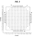
- SS-256-QAM system has a signal constellation of stepped square configuration with 18 rows extending along the Q-channel axis and 18 columns extending along the I-channel axis. Each of the rows must be discriminated by comparison with 35 decision thresholds of the Q-channel system and each of the columns must also be discriminated by comparison with 35 decision thresholds of the I-channel system.
- an analog-to-digital converter of 6 bits or more would be required.
- 2 6 comparators are required, i.e., the (n+2)-bit analog-to-digital converter requires as many as 2 n+2 comparators.
- One approach to this problem would be to compress the amplitude of the demodulated signal. However, discrimination errors will increase due to a possible reduction of signal to noise ratio.
- Another approach is to employ a 6-bit analog-to-digital converter having 63 or more decision threshold levels and a high speed read-only memory connected to the output of the 6-bit A/D converter.
- the read-only memory has data stored in locations which are addressable as a function of the input from the A/D converter, the retrieved data indicating signal points located inside or outside of a square of the signal constellation of a SS-256 QAM system.
- A/D converter is implemented by LSI technology and a substantial amount of power is dissipated.
- Another object of the invention is to provide a stepped square 2 2n -QAM demodulator including I-channel and Q-channel systems.
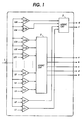
- the A/D converter comprises an array of (2 n+1 + 3) comparators C1 through C35 (where n is 4 in the case of the stepped square 256-QAM system) respectively having decision threshold levels L1 through L35 to compare the instantaneous level of an incoming I- or Q-channel demodulated signal of the QAM system applied to an input terminal 1 with their decision threshold levels.
- Each of the comparators C1 to C35 produces a logic-1 or logic-0 output depending on whether the input level is higher or lower than the decision thresholds of the comparators. It is seen in Fig. 2 that the odd-numbered decision threshold levels L1, L3 ...
- L33, L35 correspond respectively to the eighteen levels, or signal points of the I- or Q-channel signal of the SS 256-QAM system.
- the functions of four comparators C1,C2,C34,C35 are to detect signal points outside of a 16 x 16 square indicated at 4 in the signal constellation of the SS 256-QAM system as shown in Fig, 3, and the functions of (2 n+1 -1) comparators C3 to C33 are to detect signal points within the square 4.
- comparators C1 and C2 detect signal points on the leftmost column shown at 5d in the signal constellation which is located outside of the square 4, and comparators C34 and C35 detect signal points in the rightmost column 5b of the signal constellation which is also outside of square 4.
- the comparators C3 to C33 detect signal points of the 2nd to 17-th columns of the square 4.
- comparators C1 and C2 detect signal points of the lowermost row 5a of the signal constellation and comparators C34 and C35 detect signal points of the uppermost row 5c, and comparators C3 to C33 detect signal points of the 2nd to 17-th rows within the square 4.
- the logic outputs of the comparators C3 to C33 are connected to respective inputs of a first logic circuit 2 to generate a 5-bit digital signal, or 2 n+1 -bit outputs on parallel output lines a,b,c,d, and e, with the output line a being the most significant bit (MSB) and the output line e being the least significant bit (LSB).
- the rectangular waveforms of the LSB and 4SB of the 5-bit digital signal are shown in Fig. 2.
- the logic outputs of comparators C1, C2, C34 and C35 are connected to a second logic circuit 3 to produce 2-bit outputs which appear respectively on output lines f and g .
- the rectangular waveforms of the 2-bit outputs are shown in Fig.
- the output line f is at logic-1 for an input level lying between thresholds L2 and L34 and the output line g is at logic-1 for an input level lying between thresholds L1 and L35.
- the analog-to-digital converter for a stepped square 2 2n -QAM system needs (2 n+1 -1) comparators for detecting signal points inside of the outermost region of the signal constellation and four comparators for detecting the outermost signal points.
- the number of comparators employed in the present invention is therefore smaller than the conventional A/D converter having 2 n+2 comparators by 2 n+2 -(2 n+1 + 3).
- the reduction of comparators results in a reduction of power consumption and a reduction of chip size if it is implemented with LSI technology.
- a further advantage of the present invention is that it eliminates the need for a high speed read-only memory for detecting the outermost signal points to generate an error signal for feedback control.
- the analog-to-digital converter of the invention is incorporated in a stepped square QAM demodulator as shown in Fig. 4.
- the demodulator comprises a synchronous detection QAM demodulator circuit 6 which performs quadrature demodulation on an incoming 256-SS-QAM signal and produces I-channel and Q-channel demodulated signals and feeds I-channel and Q-channel systems 7i and 7q of identical construction. For simplicity, only the I-channel system is shown in detail.
- the I-channel demodulated signal is supplied to an automatic gain controller and/or dc-offset controller 8i.
- the output of controller 8i is coupled to the input of an A/D converter 9i constructed according to the present invention as described above.
- the LSB output on line e of the A/D converter 9i is supplied as an error signal e 1 to a control signal generator 10i as a representation of the deviation of the MSB to 2SB outputs on lines a to d from an optimum value and the signal on output line g is supplied as an error signal e2 to the control signal generator 10i as a representation of the deviation of the signal on output line f from optimum value.
- the MSB to 2SB outputs on lines a to d and the signal on output line f are supplied to the control signal generator 10i as well as to a coding circuit 11i which converts the inputs to a five-bit I-channel digital output.
- Control signal generator 10i counts the error signals and controls the controller 8i so that the level of the I-channel signal at the input of the A/D converter 9i is adjusted to correspond to a desired decision threshold.
- n is equal to or greater than 3.
Landscapes
- Engineering & Computer Science (AREA)
- Computer Networks & Wireless Communication (AREA)
- Signal Processing (AREA)
- Theoretical Computer Science (AREA)
- Digital Transmission Methods That Use Modulated Carrier Waves (AREA)
Claims (4)
- Convertisseur analogique/numérique pour un démodulateur à modulation en amplitude en quadrature à 22n gradins rectangulaires, où n est égal à 3 ou supérieur à 3, comprenant :
un premier groupe de 2n+1-1 comparateurs (C3 à C33) destiné à détecter les points de signal d'un signal démodulé d'un système à modulation en amplitude en quadrature à gradins rectangulaires qui sont situés à l'intérieur d'un carré de 2n x 2n de la constellation des signaux du système à modulation en amplitude en quadrature à gradins rectangulaires ;
un second groupe de quatre comparateurs (C1, C2, C34, C35) destinés à détecter les points de signal situés à l'extérieur du carré ;
un premier moyen de circuit logique (2) pour convertir les sorties des comparateurs du premier groupe en un premier signal numérique multibits représentatif des points de signal situés à l'intérieur du carré, et
un second moyen de circuit logique (3) pour convertir les sorties des comparateurs du second groupe en un second signal numérique multibits représentatif des points de signal situés à l'extérieur du carré. - Convertisseur analogique/numérique selon la revendication 1, dans lequel le bit de poids faible du premier signal numérique multibits représente une composante d'erreur du restant du premier signal numérique multibits et un bit du second signal numérique multibits représente une composante d'erreur du restant du second signal numérique multibits.
- Convertisseur analogique/numérique selon la revendication 1 ou 2, dans lequel le premier groupe de 2n+1-1 comparateurs comparent le signal démodulé à 2n+1-1 seuils de décision successivement différents de valeurs intermédiaires et produit des sorties logiques représentatives des points de signal situés à l'intérieur du carré de 2n x 2n, et le second groupe des quatre comparateurs comparent le signal démodulé à des seuils de décision successivement différents supérieurs aux valeurs intermédiaires et à des seuils de décision successivement différents inférieurs aux valeurs intermédiaires et produit des sorties logiques représentatives des points de signal situés à l'extérieur du carré.
- Démodulateur à modulation en amplitude en quadrature à 22n gradins rectangulaires, où n est égal à 3 ou supérieur à 3, comportant des systèmes à canal I et à canal Q, chacun des systèmes à canal I et à canal Q comprenant :
un moyen de commande de niveau (8i) pour commander le niveau d'un signal démodulé du système à modulation en amplitude en quadrature en réponse à un signal de commande appliqué à celui-ci ;
un convertisseur analogique/numérique (7i) comprenant un premier groupe de 2n+1-1 comparateurs pour détecter les points de signal du signal démodulé qui sont situés à l'intérieur d'un carré de 2n x 2n de la constellation des signaux du système à modulation en amplitude en quadrature à gradins rectangulaires, un second groupe de quatre comparateurs pour détecter les points de signal situés à l'extérieur du carré, un premier moyen de circuit logique pour convertir les sorties des comparateurs du premier groupe en un premier signal numérique multibits représentatif des points de signal situés à l'intérieur du carré, et un second moyen de circuit logique pour convertir les sorties des comparateurs du second groupe en un second signal numérique multibits représentatif des points de signal situés à l'extérieur du carré, le bit de poids faible du premier signal numérique multibits représentant une composante d'erreur (e₁) du restant du premier signal numérique multibits et le bit de poids faible du second signal numérique multibits représentant une composante d'erreur (e₂) du restant du second signal numérique multibits ;
un moyen (10i) pour obtenir le signal de commande à partir des premier et second signaux numériques multibits, et
un moyen (11i) pour obtenir un signal numérique à n bits à partir des restants des premier et second signaux numériques multibits.
Applications Claiming Priority (2)
| Application Number | Priority Date | Filing Date | Title |
|---|---|---|---|
| JP259284/87 | 1987-10-14 | ||
| JP62259284A JPH0693706B2 (ja) | 1987-10-14 | 1987-10-14 | アナログ−ディジタル変換器 |
Publications (3)
| Publication Number | Publication Date |
|---|---|
| EP0312047A2 EP0312047A2 (fr) | 1989-04-19 |
| EP0312047A3 EP0312047A3 (en) | 1990-05-30 |
| EP0312047B1 true EP0312047B1 (fr) | 1993-04-28 |
Family
ID=17331948
Family Applications (1)
| Application Number | Title | Priority Date | Filing Date |
|---|---|---|---|
| EP88117016A Expired - Lifetime EP0312047B1 (fr) | 1987-10-14 | 1988-10-13 | Convertisseur analogique-numérique pour démodulateurs de signaux modulés en phase et en amplitude par gradins rectangulaires |
Country Status (4)
| Country | Link |
|---|---|
| US (1) | US4912728A (fr) |
| EP (1) | EP0312047B1 (fr) |
| JP (1) | JPH0693706B2 (fr) |
| DE (1) | DE3880611T2 (fr) |
Families Citing this family (2)
| Publication number | Priority date | Publication date | Assignee | Title |
|---|---|---|---|---|
| JP2794964B2 (ja) * | 1991-02-27 | 1998-09-10 | 日本電気株式会社 | 制御信号発生回路 |
| US5640417A (en) * | 1991-10-04 | 1997-06-17 | Harris Canada, Inc. | QAM detector which compensates for received symbol distortion induced by a cellular base station |
Family Cites Families (3)
| Publication number | Priority date | Publication date | Assignee | Title |
|---|---|---|---|---|
| JPS5939149A (ja) * | 1982-08-28 | 1984-03-03 | Nec Corp | 多値直交振幅復調器 |
| US4554671A (en) * | 1983-11-04 | 1985-11-19 | Fuji Photo Film Co., Ltd. | Delta modulated communication system |
| US4571550A (en) * | 1984-06-22 | 1986-02-18 | Rockwell International Corporation | QAM Demodulator carrier recovery loop using n-m LSB's |
-
1987
- 1987-10-14 JP JP62259284A patent/JPH0693706B2/ja not_active Expired - Fee Related
-
1988
- 1988-10-12 US US07/256,701 patent/US4912728A/en not_active Expired - Lifetime
- 1988-10-13 DE DE8888117016T patent/DE3880611T2/de not_active Expired - Fee Related
- 1988-10-13 EP EP88117016A patent/EP0312047B1/fr not_active Expired - Lifetime
Also Published As
| Publication number | Publication date |
|---|---|
| JPH01101763A (ja) | 1989-04-19 |
| EP0312047A3 (en) | 1990-05-30 |
| EP0312047A2 (fr) | 1989-04-19 |
| DE3880611T2 (de) | 1993-08-05 |
| US4912728A (en) | 1990-03-27 |
| DE3880611D1 (de) | 1993-06-03 |
| JPH0693706B2 (ja) | 1994-11-16 |
Similar Documents
| Publication | Publication Date | Title |
|---|---|---|
| EP0308891B1 (fr) | Démodulateur de QAM en escalier utilisant tous les points du signal pour générer des signaux de commande | |
| US5166956A (en) | Data transmission system and apparatus providing multi-level differential signal transmission | |
| EP0180969A2 (fr) | Circuit de commande automatique de niveau pour un convertisseur analogique-numerique | |
| US5623265A (en) | Flash analog-to-digital converter and method of operation | |
| KR910009674B1 (ko) | 디지탈 복조장치 | |
| EP0163196B1 (fr) | Circuit de contrôle de signaux à niveaux multiples | |
| US4843616A (en) | Method of obtaining a phase difference signal | |
| EA000985B1 (ru) | Устройство и способ демодуляции многоуровневого сигнала | |
| CA1231397A (fr) | Dispositif de mise en forme d'ondes | |
| JPH0681164B2 (ja) | 符号変調方式 | |
| EP0254877B1 (fr) | Circuit de contrôle automatique de dérive | |
| US4456904A (en) | Analog-to-digital converter circuit | |
| US4912728A (en) | Analog-to-digital converter for stepped square QAM demodulators | |
| EP0501448A2 (fr) | Circuit de commande de gain pour démodulateur MAQ | |
| US5017918A (en) | Method and circuit for eliminating major bit transition error at the bipolar zero point in a digital-to-analog converter | |
| EP0186757A2 (fr) | Modulateur et démodulateur d'amplitude en quadrature de phase | |
| JPH0629951A (ja) | 軟判定器 | |
| US6229386B1 (en) | Digital FM demodulation circuit | |
| US6028475A (en) | Method and apparatus for demodulating multi-level QAM signal | |
| JPH0671278B2 (ja) | 復調装置 | |
| JPH09186726A (ja) | 多値信号復調装置及び多値信号復調方法 | |
| JPS6351608B2 (fr) | ||
| JP3112349B2 (ja) | アナログ−デジタルコンバータ | |
| JPH0478054B2 (fr) | ||
| KR930007651B1 (ko) | 에러 검출기능을 갖는 a/d 변환회로 |
Legal Events
| Date | Code | Title | Description |
|---|---|---|---|
| PUAI | Public reference made under article 153(3) epc to a published international application that has entered the european phase |
Free format text: ORIGINAL CODE: 0009012 |
|
| 17P | Request for examination filed |
Effective date: 19881013 |
|
| AK | Designated contracting states |
Kind code of ref document: A2 Designated state(s): DE FR GB |
|
| PUAL | Search report despatched |
Free format text: ORIGINAL CODE: 0009013 |
|
| AK | Designated contracting states |
Kind code of ref document: A3 Designated state(s): DE FR GB |
|
| 17Q | First examination report despatched |
Effective date: 19920601 |
|
| GRAA | (expected) grant |
Free format text: ORIGINAL CODE: 0009210 |
|
| AK | Designated contracting states |
Kind code of ref document: B1 Designated state(s): DE FR GB |
|
| REF | Corresponds to: |
Ref document number: 3880611 Country of ref document: DE Date of ref document: 19930603 |
|
| ET | Fr: translation filed | ||
| PLBE | No opposition filed within time limit |
Free format text: ORIGINAL CODE: 0009261 |
|
| STAA | Information on the status of an ep patent application or granted ep patent |
Free format text: STATUS: NO OPPOSITION FILED WITHIN TIME LIMIT |
|
| 26N | No opposition filed | ||
| REG | Reference to a national code |
Ref country code: GB Ref legal event code: IF02 |
|
| PGFP | Annual fee paid to national office [announced via postgrant information from national office to epo] |
Ref country code: FR Payment date: 20021008 Year of fee payment: 15 |
|
| PGFP | Annual fee paid to national office [announced via postgrant information from national office to epo] |
Ref country code: GB Payment date: 20021009 Year of fee payment: 15 |
|
| PGFP | Annual fee paid to national office [announced via postgrant information from national office to epo] |
Ref country code: DE Payment date: 20021017 Year of fee payment: 15 |
|
| PG25 | Lapsed in a contracting state [announced via postgrant information from national office to epo] |
Ref country code: GB Free format text: LAPSE BECAUSE OF NON-PAYMENT OF DUE FEES Effective date: 20031013 |
|
| PG25 | Lapsed in a contracting state [announced via postgrant information from national office to epo] |
Ref country code: DE Free format text: LAPSE BECAUSE OF NON-PAYMENT OF DUE FEES Effective date: 20040501 |
|
| GBPC | Gb: european patent ceased through non-payment of renewal fee |
Effective date: 20031013 |
|
| PG25 | Lapsed in a contracting state [announced via postgrant information from national office to epo] |
Ref country code: FR Free format text: LAPSE BECAUSE OF NON-PAYMENT OF DUE FEES Effective date: 20040630 |
|
| REG | Reference to a national code |
Ref country code: FR Ref legal event code: ST |