EP0312088A2 - Thyristor sensible ayant une immunité au bruit améliorée - Google Patents
Thyristor sensible ayant une immunité au bruit améliorée Download PDFInfo
- Publication number
- EP0312088A2 EP0312088A2 EP88117118A EP88117118A EP0312088A2 EP 0312088 A2 EP0312088 A2 EP 0312088A2 EP 88117118 A EP88117118 A EP 88117118A EP 88117118 A EP88117118 A EP 88117118A EP 0312088 A2 EP0312088 A2 EP 0312088A2
- Authority
- EP
- European Patent Office
- Prior art keywords
- type
- thyristor
- region
- base region
- gate
- Prior art date
- Legal status (The legal status is an assumption and is not a legal conclusion. Google has not performed a legal analysis and makes no representation as to the accuracy of the status listed.)
- Granted
Links
Images


Classifications
-
- H—ELECTRICITY
- H10—SEMICONDUCTOR DEVICES; ELECTRIC SOLID-STATE DEVICES NOT OTHERWISE PROVIDED FOR
- H10D—INORGANIC ELECTRIC SEMICONDUCTOR DEVICES
- H10D84/00—Integrated devices formed in or on semiconductor substrates that comprise only semiconducting layers, e.g. on Si wafers or on GaAs-on-Si wafers
- H10D84/01—Manufacture or treatment
- H10D84/0102—Manufacture or treatment of thyristors having built-in components, e.g. thyristor having built-in diode
-
- H—ELECTRICITY
- H10—SEMICONDUCTOR DEVICES; ELECTRIC SOLID-STATE DEVICES NOT OTHERWISE PROVIDED FOR
- H10D—INORGANIC ELECTRIC SEMICONDUCTOR DEVICES
- H10D84/00—Integrated devices formed in or on semiconductor substrates that comprise only semiconducting layers, e.g. on Si wafers or on GaAs-on-Si wafers
- H10D84/101—Integrated devices comprising main components and built-in components, e.g. IGBT having built-in freewheel diode
- H10D84/131—Thyristors having built-in components
- H10D84/133—Thyristors having built-in components the built-in components being capacitors or resistors
-
- H—ELECTRICITY
- H10—SEMICONDUCTOR DEVICES; ELECTRIC SOLID-STATE DEVICES NOT OTHERWISE PROVIDED FOR
- H10D—INORGANIC ELECTRIC SEMICONDUCTOR DEVICES
- H10D84/00—Integrated devices formed in or on semiconductor substrates that comprise only semiconducting layers, e.g. on Si wafers or on GaAs-on-Si wafers
- H10D84/101—Integrated devices comprising main components and built-in components, e.g. IGBT having built-in freewheel diode
- H10D84/131—Thyristors having built-in components
- H10D84/138—Thyristors having built-in components the built-in components being FETs
-
- H—ELECTRICITY
- H10—SEMICONDUCTOR DEVICES; ELECTRIC SOLID-STATE DEVICES NOT OTHERWISE PROVIDED FOR
- H10F—INORGANIC SEMICONDUCTOR DEVICES SENSITIVE TO INFRARED RADIATION, LIGHT, ELECTROMAGNETIC RADIATION OF SHORTER WAVELENGTH OR CORPUSCULAR RADIATION
- H10F30/00—Individual radiation-sensitive semiconductor devices in which radiation controls the flow of current through the devices, e.g. photodetectors
- H10F30/20—Individual radiation-sensitive semiconductor devices in which radiation controls the flow of current through the devices, e.g. photodetectors the devices having potential barriers, e.g. phototransistors
- H10F30/21—Individual radiation-sensitive semiconductor devices in which radiation controls the flow of current through the devices, e.g. photodetectors the devices having potential barriers, e.g. phototransistors the devices being sensitive to infrared, visible or ultraviolet radiation
- H10F30/26—Individual radiation-sensitive semiconductor devices in which radiation controls the flow of current through the devices, e.g. photodetectors the devices having potential barriers, e.g. phototransistors the devices being sensitive to infrared, visible or ultraviolet radiation the devices having three or more potential barriers, e.g. photothyristors
- H10F30/263—Photothyristors
-
- H—ELECTRICITY
- H10—SEMICONDUCTOR DEVICES; ELECTRIC SOLID-STATE DEVICES NOT OTHERWISE PROVIDED FOR
- H10F—INORGANIC SEMICONDUCTOR DEVICES SENSITIVE TO INFRARED RADIATION, LIGHT, ELECTROMAGNETIC RADIATION OF SHORTER WAVELENGTH OR CORPUSCULAR RADIATION
- H10F39/00—Integrated devices, or assemblies of multiple devices, comprising at least one element covered by group H10F30/00, e.g. radiation detectors comprising photodiode arrays
- H10F39/10—Integrated devices
- H10F39/103—Integrated devices the at least one element covered by H10F30/00 having potential barriers, e.g. integrated devices comprising photodiodes or phototransistors
Definitions
- This invention relates to a semiconductor device having a main thyristor and an auxiliary thyristor (which is also called a pilot thyristor) formed in a single semiconductor substrate, and more particularly to a sensitive thyristor having an improved noise-capability.
- a thyristor is widely used to effect various control operations such as ON/OFF control of electric power.
- the basic structure of the thyristor is explained in the article by ADOLPH BLICHER in "Thyristor Physics" pp. 1 to 13.
- the thyristor in the OFF state is made conductive when a gate current is increased to a certain value with a preset voltage kept applied between the anode and cathode.
- the minimum gate current required for turning on the thyristor is called gate turn-on current I GT , and the sensitivity of the thyristor becomes higher when current I GT is set to be smaller.
- Gate turn-on current I GT is controlled by various methods so as to attain a desired ON characteristic.
- the thyristor When an abruptly rising noise voltage is applied between the anode and cathode of the thyristor in the OFF state, the thyristor may be turned on (erroneously triggered) even if no gate current is supplied.
- the turn-on operation is considered to occur as explained below.
- a junction capacitor between the P-type base region and N-type base region of the thyristor is charged by application of the noise voltage.
- a displacement current "Cdv/dt" (C is a capacitance of the junction capacitor) will flow over the entire surface of the junction area.
- the displacement current has substantially the same effect as the gate current, and at this time, the thyristor is turned on.
- critical off voltage rising rate voltage variation rate dv/dt immediately before the thyristor is turned on
- the critical off voltage rising rate is larger, the possibility of the thyristor to be turned on by the noise voltage becomes smaller, and therefore it is preferable to set the critical off voltage rising rate to be larger.
- the above phenomena are generally called dv/dt characteristics.
- the dv/dt characteristics and sensitivity of the thyristor are incompatible with each other. That is, when the sensitivity is set to be high, the dv/dt characteristic will be deteriorated, and when the dv/dt characteristic is enhanced, the sensitivity is lowered.
- an amplifying gate type thyristor can be used to effect a method for controlling the ON and OFF conditions of a thyristor which is operated with a large driving ability (current capacity) by a small gate current.
- a thyristor is disclosed in "Thyristor Physics" pp. 120-121.
- the amplifying gate type thyristor includes a main thyristor having a large driving ability (requiring large gate turn-on current I GT ) and an auxiliary thyristor having a small driving ability (which can be turned on by small gate turn-on current I GT ).
- the main thyristor is constituted to have a cathode formed in the form of shorted emitter structure in order to enhance the dv/dt characteristic.
- the cathode of the auxiliary thyristor is connected to the gate of the main thyristor, and the anode thereof is connected to the anode of the main thyristor.
- the main thyristor having the large driving ability (current capacity) can be turned on by a relatively small gate current.
- the dv/dt characteristic is not sufficiently improved. This is because the main thyristor will be turned on when the highly sensitive auxiliary thyristor is turned on by a noise voltage even if the dv/dt characteristic of the main thyristor is sufficiently improved.
- the P-type base region of the main thyristor is electrically connected to the P-type base region of the auxiliary thyristor.
- the highly sensitive auxiliary thyristor may be turned on even if the main thyristor having the sufficiently improved dv/dt characteristic is not turned on at this time.
- the dv/dt characteristic of the amplifying gate type thyristor largely depends on the dv/dt characteristic of the auxiliary thyristor.
- An object of this invention is to provide a thyristor having a high gate sensitivity and improved noise-capability.
- a thyristor comprising a main thyristor formed in a semiconductor substrate; an auxiliary thyristor formed in the same semiconductor substrate in which the main thyristor is formed and functioning to control the operation of the main thyristor; a MOSFET formed between the main thyristor and the auxiliary thyristor; and an energization circuit for energizing the gates of the MOSFET and the auxiliary thyristor.
- the main and auxiliary thyristors are separated from each other when the MOSFET is in the OFF state. Therefore, even if a noise voltage is applied to thyristors, the main thyristor will not be turned on. Further, when the MOSFET is in the ON state, the main and auxiliary thyristors are connected to each other. Therefore, if the auxiliary thyristor is turned on, the main thyristor is also turned on.
- a thyristor which has high gate sensitivity and high noise-capability can be provided.
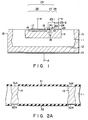
- Fig. 1 is a cross sectional view of a thyristor according to a first embodiment of this invention.
- P-type emitter region 12 acting as an anode is formed in the rear surface area of N-type semiconductor substrate (N-type base region) 11.
- Anode electrode 13 is formed in ohmic contact with P-type emitter region 12.
- Anode terminal A is connected to anode electrode 13.
- P-type base region 14 acting as a gate is formed in the front surface area of semiconductor substrate 11.
- Isolation regions 15 are formed from the front surface to the rear surface of semiconductor substrate 11 to surround P-type base region 14.
- First N-type emitter region 16 acting as a cathode is formed in the surface area of P-type base region 14.
- Cathode electrode 17 is formed in ohmic contact with first N-type emitter region 16.
- Cathode terminal K is connected to cathode electrode 17.
- Second N-type emitter region 18 is formed separately from and deeper than first N-type emitter region 16 in the surface area of P-type base region 14.
- Gate electrode 20 of MOSFET 19 is formed on gate insulation film 21 which is formed on that portion of P-type base region 14 which lies between first and second N-type emitter regions 16 and 18.
- N-type impurity region 22 is formed separately from first and second N-type emitter regions 16 and 18 in the surface area of P-type base region 14.
- Gate terminal G is connected to gate electrode 20 by use of wiring layer 23-1 and to N-type impurity region 22 by use of wiring layer 23-2. Further, gate terminal G is connected to one end of resistor 24 which is connected at the other end to gate electrode 25 of a thyristor formed in ohmic contact with P-type base region 14.
- Main thyristor 26 with PNPN structure is constituted by P-type emitter region 12, N-type semiconductor substrate (N-type base region) 11, P-type base region 14 and first N-type emitter region 16. Further, auxiliary thyristor 27 with PNPN structure is constituted by P-type emitter region 12, N-type semiconductor substrate (N-type base region) 11, P-type base region 14 and second N-type emitter region 18. Since second N-type emitter region 18 of auxiliary thyristor 27 is formed deeper than first N-type emitter region 16, the sensitivity of auxiliary thyristor 27 is set to be higher than that of main thyristor 26.
- MOSFET 19 includes first and second N-type emitter regions 16 and 18, P-type base region 14, gate insulation film 21 and gate electrode 20.
- First and second N-type emitter regions 16 and 18 act as source and drain regions, and that portion of P-type base region 14 which lies between first and second N-type emitter regions 16 and 18 acts as a channel region.
- Zener diode 28 is formed of P-type base region 14 and N-type impurity region 22, and is used to protect the gate insulation film of MOSFET 19.
- Figs. 2A to 2E are cross sectional views sequentially showing the manufacturing steps of manufacturing the thyristor shown in Fig. 1.
- oxide films 31 and 32 are respectively formed on the front and rear surfaces of N-type semiconductor substrate (silicon substrate) 11 with the resistivity of 40 ⁇ cm.
- Semiconductor substrate 11 is used as an N-type base region.
- Openings 31A and 31B are formed by a PEP method in portions of oxide film 31 corresponding in position to the area in which isolation regions 15 are formed.
- openings 32A and 32B are formed by a PEP method in portions of oxide film 32 corresponding in position to the area in which isolation regions 15 are formed.
- P-type impurity is doped into semiconductor substrate 11 via openings 31A, 31B, 32A and 32B from both sides of semiconductor substrate 11 so as to form isolation regions 15.
- oxide films 31 and 32 are removed and then oxide film 33 is formed on the upper surface of the resultant semiconductor structure.
- Part of oxide film 33 which lies on the formation area for formation of P-type base region 14 is selectively removed by a PEP method.
- a P-type impurity is doped into semiconductor substrate 11 from the both sides thereof with oxide film 33 used as a mask.
- boron is deposited to the exposed surface of semiconductor substrate 11 in a heat treatment process at a temperature of 1000°C for approx. one hour and is diffused to a depth of 40 ⁇ m.
- P-type emitter region 12 and P-type base region 14 with a surface impurity concentration of 1 x 10¹⁸ to 5 x 10¹⁸ atoms/cm3 can be formed at the same time.
- an N-type impurity is selectively ion-implanted into a portion of P-type base region 14 which lies in position corresponding to an area for formation of the channel region of MOSFET 19 so as to form impurity region 14A whose P-type impurity concentration is reduced to approx. 1 x 10¹⁷ atoms/cm3.
- Openings 34A is formed by a PEP method in a portion of oxide film 34 corresponding in position to the area for formation of second N-type emitter region 18. Then, an N-type impurity is doped into the surface area of semiconductor substrate 11 with oxide films 34 and 35 used as a mask. Subsequently, openings 34B and 34C are formed by a PEP method in those portions of oxide film 34 which lie on the areas for formation of first N-type emitter region 16 and N-type impurity region 22. Then, an N-type impurity is doped into the surface area of semiconductor substrate 11 with oxide films 34 and 35 used as a mask.
- phosphor is adhered to the exposed surface of semiconductor substrate 11 in a heat treatment process at a temperature of 1100°C for approx. 30 minutes and is diffused to a depth of 12 ⁇ m.
- first N-type emitter region 16, second N-type emitter region 18 and N-type impurity region 22 with a surface impurity concentration of 1 x 10²¹ atoms/cm3 or more can be formed. Since impurity doping steps are effected twice to form second N-type emitter region 18, the diffusion depth thereof becomes deep and as a result the construction shown in Fig. 2C can be obtained.
- oxide film 34 is selectively removed, and a thin oxide film used as gate insulation film 21 is formed on that portion of P-type base region 14 which lies between first and second N-type emitter regions 16 and 18.
- a polysilicon layer is formed on gate insulation film 21 and oxide film 34, the polysilicon layer is patterned to form gate electrode 20 and resistor 24. The resistance value of the resistor 24 is controlled by ion-implantation technique.
- oxide film 36 is formed on the surface of the resultant semiconductor structure as shown in Fig. 2D.
- openings 36A, 36B, 36C, 36D and 36E are formed by a PEP method in oxide film 36 in positions corresponding to first N-type emitter region 16, N-type impurity region 22, P-type base region 14 and ends of resistor 24, and oxide film 35 is removed. Then, metal such as aluminum is vapor deposited on both surfaces of the resultant semiconductor structure and is patterned. As a result, anode electrode 13, cathode electrode 17, cathode extraction electrode 37 of a Zener diode, gate electrode 25 and gate extraction electrode 38 of a thyristor are formed as shown in Fig. 2E.
- semiconductor substrate 11 is cut along X-X′ lines in Fig. 2E, and then anode electrode 13 and cathode electrode 17 are connected to anode terminal A and cathode terminal K, respectively.
- Gate electrode 20 of MOSFET 19 and electrode 37 are connected to gate terminal G via wiring layers 23-1 and 23-2, respectively.
- gate extraction electrode 38 is connected to gate terminal G to form a thyristor shown in Fig. 1.
- main thyristor 26 In a case where no voltage is applied to gate terminal G, main thyristor 26, auxiliary thyristor 27 and MOSFET 19 are all turned off. In this case, since main thyristor is constituted to have an improved dv/dt characteristic, main thyristor 26 is not easily turned on even if a noise voltage is applied between anode terminal A and cathode terminal K. Further, since auxiliary thyristor 27 is separated from main thyristor 26 by means of MOSFET 19 which is now in the OFF state, main thyristor 26 will not be turned on.
- main thyristor 26 and auxiliary thyristor 27 are connected to each other.
- main thyristor 26 and auxiliary thyristor 27 are combined to function as one thyristor 29 having a high gate sensitivity area (auxiliary thyristor section 27).
- a gate current flows from gate terminal G to P-type base region 14 or the gate of auxiliary thyristor 27 via resistor 24.
- auxiliary thyristor 27 is turned on.
- auxiliary thyristor 27 The effect due to the turn-on of auxiliary thyristor 27 is transferred to main thyristor 26 via MOSFET 19, and main thyristor 26 is also turned on. Since the threshold voltage of MOSFET 19 is approx. 1.5 V and voltage V GT for turning on auxiliary thyristor 27 is 0.5 V, it is sufficient to set a voltage applied to gate terminal G when auxiliary thyristor 27 is turned on to approx. 2 V. At this time, gate turn-on current I GT of auxiliary thyristor 27 is approx. 10 ⁇ A and auxiliary thyristor 27 is sufficiently sensitive. Resistor 24 is used to adjust threshold voltage V TH of auxiliary thyristor 28 and gate turn-on voltage V GT so as to attain an adequate gate current. Further, breakdown occurs in Zener diode 28 when a high voltage is applied to gate terminal G so that gate insulation film 21 of MOSFET 19 can be effectively prevented from being damaged.
- Fig. 3 shows a modification of the thyristor shown in Fig. 1.
- the thyristor is triggered by irradiation of light. That is, in the thyristor of Fig. 1, auxiliary thyristor 27 is triggered by applying voltage to gate terminal G and supplying a gate current to auxiliary thyristor 27 via resistor 24.
- the thyristor shown in Fig. 3 is triggered by irradiation of light.
- portions which are similar to those of the thyristor shown in Fig. 1 are denoted by the same reference numerals and the explanation therefor is omitted.
- photodiodes 41 and 42 are embedded in that portion of P-type base region 14 which lies between second N-type emitter region 18 and N-type impurity region 22. Photodiodes 41 and 42 are isolated from P-type base region 14 by means of insulation films 43 and 44, respectively. Photodiodes 41 and 42 are respectively formed of P-type impurity regions 45 and 46 acting as an anode region and N-type impurity regions 47 and 48 formed in the surface area of respective impurity regions 45 and 46.
- P-type impurity region 45 of photodiode 41 is connected to gate electrode 20 of MOSFET 19, and N-type impurity region 47 of photodiode 41 is connected to P-type impurity region 46 of photodiode 42. Further, N-type impurity region 48 of photodiode 42 is connected to P-type base region 14.
- Fig. 4 shows a thyristor according to a second embodiment of this invention.
- the thyristor is constructed by applying this invention to the amplifying gate type thyristor.
- P-type emitter region 12 acting as an anode is formed in the rear surface area of N-type semiconductor substrate (N-type base region) 11.
- Anode electrode 13 is formed in ohmic contact with P-type emitter region 12.
- Anode terminal A is connected to anode electrode 13.
- First P-type base region 14-1 acting as a gate of the main thyristor is formed in the front surface area of semiconductor substrate 11.
- Second P-type base region 14-2 acting as a gate of the auxiliary thyristor is formed separately from P-type base region 14-1 in the front surface area of semiconductor substrate 11.
- Isolation regions 15 are formed from the front surface to the rear surface of semiconductor substrate 11 to surround first and second P-type base regions 14-1 and 14-2.
- First to third N-type emitter regions 16-1 to 16-3 acting as a cathode of the main thyristor is formed in the surface area of P-type base region 14-1.
- Cathode electrode 17 is formed in ohmic contact with first to third N-type emitter regions 16-1 to 16-3.
- Cathode terminal K is connected to cathode electrode 17.
- Fourth N-type emitter region 18 is formed in the surface area of second P-type base region 14-2.
- N-type impurity region 51 is formed separately from fourth N-type emitter region 18 in the surface area of second P-type base region 14-2.
- N-type impurity region 51 is connected to gate electrode 53 of the main thyristor which is ohmic contact with first P-type base region 14-1 via wiring layer 52.
- Gate electrode 20 of MOSFET 19 is formed on gate insulation film 21 which is formed on that portion of second P-type base region 14-2 which lies between fourth N-type emitter region 18 and N-type impurity region 51.
- N-type impurity region 22 is formed separately from fourth N-type emitter region 18 and N-type impurity region 51 in the surface area of second P-type base region 14-2.
- Gate terminal G is connected to gate electrode 20 by use of wiring layer 23-1 and to N-type impurity region 22 by use of wiring layer 23-2. Further, gate terminal G is connected to one end of resistor 24 which is connected at the other end to gate electrode 25 of an auxiliary thyristor formed in ohmic contact with second P-type base region 14-2.
- Main thyristor 26 with PNPN structure is constituted by P-type emitter region 12, N-type semiconductor substrate (N-type base region) 11, first P-type base region 14-1 and first to third N-type emitter regions 16-1 to 16-3.
- main thyristor 26 has a shorted emitter structure.
- auxiliary thyristor 27 with PNPN structure is constituted by P-type emitter region 12, N-type semiconductor substrate (N-type base region) 11, second P-type base region 14-2 and fourth N-type emitter region 18.
- Main thyristor 26 is formed to have a shorted emitter structure and has an enhanced dv/dt characteristic.
- auxiliary thyristor 27 is formed to have a high sensitivity.
- MOSFET 19 includes fourth N-type emitter region 18, N-type impurity region 51, second P-type base region 14-2, gate insulation film 21 and gate electrode 20.
- Fourth N-type emitter region 18 and N-type impurity region 51 act as source and drain regions, and that portion of second P-type base region 4-2 which lies between fourth N-type emitter region 18 and N-type impurity regions 51 acts as a channel region.
- Zener diode 28 is formed of second P-type base region 14-2 and N-type impurity region 22, and is used to protect gate insulation film 21 of MOSFET 19.
- thyristor shown in Fig. 4 The operation is similar to that of the thyristor shown in Fig. 1 except the turn-on process of main thyristor 26.
- main thyristor 26, auxiliary thyristor 27 and MOSFET 19 are all set in the OFF condition. That is, at this time, main thyristor 26 and auxiliary thyristor 27 are electrically separated from each other by MOSFET 19 which is in the OFF condition.
- main thyristor 26 which has an enhanced dv/dt characteristic is not easily turned on.
- auxiliary thyristor 27 which is sensitive may be turned on and is thus erroneously triggered.
- MOSFET 19 since MOSFET 19 is turned off, no gate current is supplied to gate electrode 53 (first P-type base region 14-1) of main thyristor 26. As a result, main thyristor 26 will not be erroneously triggered even when auxiliary thyristor 27 is erroneously triggered.
- MOSFET 19 In a case where a voltage is applied to gate terminal G MOSFET 19 is turned on so that gate electrode 53 of main thyristor 26 and the cathode (N-type emitter region 18) of auxiliary thyristor 27 can be electrically connected via the current path of MOSFET 19 and wiring layer 52. At this time, a gate current is supplied to gate electrode 25 of auxiliary thyristor 27 via resistor 24 by application of voltage to gate terminal G. As a result, auxiliary thyristor 27 is turned on.
- auxiliary thyristor 27 causes a current flowing between the anode and cathode of auxiliary thyristor 27 to be supplied as a gate current of main thyristor 26, thereby turning on main thyristor 26.
- the inventors of this invention made for experiment the conventional amplifying gate type thyristor and a thyristor with the construction shown in Fig. 4, both thyristors being formed to have rated current and voltage of 10 A and 600 V.
- gate turn-on current I GT of 10 ⁇ A and dv/dt of 400 V/ ⁇ s were obtained when the resistance of resistor 24 was set to 200 K ⁇ .
- gate turn-on current I GT of 100 ⁇ A and dv/dt of 200 V/ ⁇ s were obtained when the resistance of an input resistor (corresponding to resistor 24 used in this invention) was set to 200 K ⁇ .
- Fig. 5 shows a modification of the thyristor shown in Fig. 4.
- the thyristor is triggered by irradiate of light, and is formed by combining the structures of Figs. 3 and 4.
- the turn-on mechanism of auxiliary thyristor 27 by application of light is the same as that of Fig. 3, and the basic operation of the thyristor is the same as that of the thyristor shown in Fig. 4. Therefore, portions which are the same as those in Figs. 3 and 4 are denoted by the same reference numerals and the explanation thereof is omitted.
- a thyristor having a high gate sensitivity and improved noise-capability can be provided.
Landscapes
- Thyristors (AREA)
- Electronic Switches (AREA)
Applications Claiming Priority (2)
| Application Number | Priority Date | Filing Date | Title |
|---|---|---|---|
| JP62260869A JP2633585B2 (ja) | 1987-10-16 | 1987-10-16 | 半導体装置 |
| JP260869/87 | 1987-10-16 |
Publications (3)
| Publication Number | Publication Date |
|---|---|
| EP0312088A2 true EP0312088A2 (fr) | 1989-04-19 |
| EP0312088A3 EP0312088A3 (fr) | 1990-12-27 |
| EP0312088B1 EP0312088B1 (fr) | 1996-12-11 |
Family
ID=17353881
Family Applications (1)
| Application Number | Title | Priority Date | Filing Date |
|---|---|---|---|
| EP88117118A Expired - Lifetime EP0312088B1 (fr) | 1987-10-16 | 1988-10-14 | Thyristor sensible ayant une immunité au bruit améliorée |
Country Status (4)
| Country | Link |
|---|---|
| US (1) | US4982259A (fr) |
| EP (1) | EP0312088B1 (fr) |
| JP (1) | JP2633585B2 (fr) |
| DE (1) | DE3855701T2 (fr) |
Cited By (4)
| Publication number | Priority date | Publication date | Assignee | Title |
|---|---|---|---|---|
| GB2303965A (en) * | 1995-07-31 | 1997-03-05 | Ixys Corp | Reverse blocking IGBT |
| DE19857673C1 (de) * | 1998-12-14 | 2000-05-04 | Siemens Ag | Leistungshalbleiterbauelement mit Randabschluß |
| EP1524700A1 (fr) * | 2003-10-17 | 2005-04-20 | St Microelectronics S.A. | Commutateur à commande isolée |
| US6936908B2 (en) | 2001-05-03 | 2005-08-30 | Ixys Corporation | Forward and reverse blocking devices |
Families Citing this family (1)
| Publication number | Priority date | Publication date | Assignee | Title |
|---|---|---|---|---|
| EP1427107B1 (fr) * | 2002-12-04 | 2011-09-14 | STMicroelectronics S.A. | Commutateur de type SCR commande en HF |
Family Cites Families (9)
| Publication number | Priority date | Publication date | Assignee | Title |
|---|---|---|---|---|
| JPS5629458B2 (fr) * | 1973-07-02 | 1981-07-08 | ||
| SE392783B (sv) * | 1975-06-19 | 1977-04-18 | Asea Ab | Halvledaranordning innefattande en tyristor och en felteffekttransistordel |
| JPS553694A (en) * | 1978-06-16 | 1980-01-11 | Motorola Inc | Device for triggering monolithic semiconductor |
| JPS5552458A (en) * | 1978-10-12 | 1980-04-16 | Matsushita Electric Works Ltd | Eaves gutter and making method thereof |
| JPS56110263A (en) * | 1980-02-04 | 1981-09-01 | Oki Electric Ind Co Ltd | Thyristor element |
| JPS56110254A (en) * | 1980-02-04 | 1981-09-01 | Oki Electric Ind Co Ltd | Pnpn semiconductor switch |
| DE3112942A1 (de) * | 1981-03-31 | 1982-10-07 | Siemens AG, 1000 Berlin und 8000 München | Thyristor und verfahren zu seinem betrieb |
| DE3112941A1 (de) * | 1981-03-31 | 1982-10-07 | Siemens AG, 1000 Berlin und 8000 München | Thyristor mit innerer stromverstaerkung und verfahren zu seinem betrieb |
| JPS60115263A (ja) * | 1983-11-28 | 1985-06-21 | Toshiba Corp | 半導体装置 |
-
1987
- 1987-10-16 JP JP62260869A patent/JP2633585B2/ja not_active Expired - Lifetime
-
1988
- 1988-10-14 US US07/257,673 patent/US4982259A/en not_active Expired - Lifetime
- 1988-10-14 DE DE3855701T patent/DE3855701T2/de not_active Expired - Lifetime
- 1988-10-14 EP EP88117118A patent/EP0312088B1/fr not_active Expired - Lifetime
Cited By (9)
| Publication number | Priority date | Publication date | Assignee | Title |
|---|---|---|---|---|
| GB2303965A (en) * | 1995-07-31 | 1997-03-05 | Ixys Corp | Reverse blocking IGBT |
| US5698454A (en) * | 1995-07-31 | 1997-12-16 | Ixys Corporation | Method of making a reverse blocking IGBT |
| US6091086A (en) * | 1995-07-31 | 2000-07-18 | Ixys Corporation | Reverse blocking IGBT |
| GB2303965B (en) * | 1995-07-31 | 2000-08-30 | Ixys Corp | Reverse blocking IGBT |
| DE19857673C1 (de) * | 1998-12-14 | 2000-05-04 | Siemens Ag | Leistungshalbleiterbauelement mit Randabschluß |
| US6936908B2 (en) | 2001-05-03 | 2005-08-30 | Ixys Corporation | Forward and reverse blocking devices |
| US7442630B2 (en) | 2001-05-03 | 2008-10-28 | Ixys Corporation | Method for fabricating forward and reverse blocking devices |
| EP1524700A1 (fr) * | 2003-10-17 | 2005-04-20 | St Microelectronics S.A. | Commutateur à commande isolée |
| FR2861229A1 (fr) * | 2003-10-17 | 2005-04-22 | St Microelectronics Sa | Commutateur scr a commande hf isole |
Also Published As
| Publication number | Publication date |
|---|---|
| DE3855701D1 (de) | 1997-01-23 |
| EP0312088A3 (fr) | 1990-12-27 |
| US4982259A (en) | 1991-01-01 |
| JPH01102963A (ja) | 1989-04-20 |
| JP2633585B2 (ja) | 1997-07-23 |
| DE3855701T2 (de) | 1997-05-07 |
| EP0312088B1 (fr) | 1996-12-11 |
Similar Documents
| Publication | Publication Date | Title |
|---|---|---|
| US4689647A (en) | Conductivity modulated field effect switch with optimized anode emitter and anode base impurity concentrations | |
| JP3911566B2 (ja) | Mos型半導体装置 | |
| US4145703A (en) | High power MOS device and fabrication method therefor | |
| US6413806B1 (en) | Semiconductor device and method for protecting such device from a reversed drain voltage | |
| JP3180831B2 (ja) | 絶縁ゲート制御半導体装置 | |
| EP0057024B1 (fr) | Dispositif semiconducteur comportant un dispositif de sécurité | |
| US4755697A (en) | Bidirectional output semiconductor field effect transistor | |
| US4721986A (en) | Bidirectional output semiconductor field effect transistor and method for its maufacture | |
| US6091107A (en) | Semiconductor devices | |
| US8339758B2 (en) | Transient voltage suppressor and method | |
| KR920010314B1 (ko) | 반도체 장치 | |
| US20090273868A1 (en) | Transient voltage suppressor and method | |
| EP0228107B1 (fr) | Transistors latéraux à grille isolée commutant rapidement | |
| EP0338312B1 (fr) | Transistor bipolaire à grille isolée | |
| US5587595A (en) | Lateral field-effect-controlled semiconductor device on insulating substrate | |
| JP3424579B2 (ja) | 半導体装置 | |
| EP0341730B1 (fr) | Dispositif de commande semi-conducteur bidirectionnel commandé par une grille | |
| US5621229A (en) | Semiconductor device and control method | |
| EP0125138B1 (fr) | Thyristor autoprotecteur et procédé de fabrication | |
| EP0312088A2 (fr) | Thyristor sensible ayant une immunité au bruit améliorée | |
| US5949128A (en) | Bipolar transistor with MOS-controlled protection for reverse-biased emitter-base junction | |
| JP4431761B2 (ja) | Mos型半導体装置 | |
| JPH0138380B2 (fr) | ||
| US5212396A (en) | Conductivity modulated field effect transistor with optimized anode emitter and anode base impurity concentrations | |
| US6064080A (en) | Semiconductor device |
Legal Events
| Date | Code | Title | Description |
|---|---|---|---|
| PUAI | Public reference made under article 153(3) epc to a published international application that has entered the european phase |
Free format text: ORIGINAL CODE: 0009012 |
|
| 17P | Request for examination filed |
Effective date: 19881014 |
|
| AK | Designated contracting states |
Kind code of ref document: A2 Designated state(s): DE FR GB |
|
| PUAL | Search report despatched |
Free format text: ORIGINAL CODE: 0009013 |
|
| AK | Designated contracting states |
Kind code of ref document: A3 Designated state(s): DE FR GB |
|
| 17Q | First examination report despatched |
Effective date: 19911004 |
|
| GRAG | Despatch of communication of intention to grant |
Free format text: ORIGINAL CODE: EPIDOS AGRA |
|
| GRAH | Despatch of communication of intention to grant a patent |
Free format text: ORIGINAL CODE: EPIDOS IGRA |
|
| GRAH | Despatch of communication of intention to grant a patent |
Free format text: ORIGINAL CODE: EPIDOS IGRA |
|
| GRAA | (expected) grant |
Free format text: ORIGINAL CODE: 0009210 |
|
| AK | Designated contracting states |
Kind code of ref document: B1 Designated state(s): DE FR GB |
|
| REF | Corresponds to: |
Ref document number: 3855701 Country of ref document: DE Date of ref document: 19970123 |
|
| ET | Fr: translation filed | ||
| ET | Fr: translation filed |
Free format text: CORRECTIONS |
|
| PLBE | No opposition filed within time limit |
Free format text: ORIGINAL CODE: 0009261 |
|
| STAA | Information on the status of an ep patent application or granted ep patent |
Free format text: STATUS: NO OPPOSITION FILED WITHIN TIME LIMIT |
|
| 26N | No opposition filed | ||
| REG | Reference to a national code |
Ref country code: GB Ref legal event code: IF02 |
|
| PGFP | Annual fee paid to national office [announced via postgrant information from national office to epo] |
Ref country code: DE Payment date: 20071011 Year of fee payment: 20 |
|
| PGFP | Annual fee paid to national office [announced via postgrant information from national office to epo] |
Ref country code: FR Payment date: 20071009 Year of fee payment: 20 Ref country code: GB Payment date: 20071010 Year of fee payment: 20 |
|
| REG | Reference to a national code |
Ref country code: GB Ref legal event code: PE20 Expiry date: 20081013 |
|
| PG25 | Lapsed in a contracting state [announced via postgrant information from national office to epo] |
Ref country code: GB Free format text: LAPSE BECAUSE OF EXPIRATION OF PROTECTION Effective date: 20081013 |