EP0312202A1 - Verfahren zur Herstellung eines Kristalls - Google Patents
Verfahren zur Herstellung eines Kristalls Download PDFInfo
- Publication number
- EP0312202A1 EP0312202A1 EP88307859A EP88307859A EP0312202A1 EP 0312202 A1 EP0312202 A1 EP 0312202A1 EP 88307859 A EP88307859 A EP 88307859A EP 88307859 A EP88307859 A EP 88307859A EP 0312202 A1 EP0312202 A1 EP 0312202A1
- Authority
- EP
- European Patent Office
- Prior art keywords
- nucleation
- crystal
- crystal formation
- substrate
- formation method
- Prior art date
- Legal status (The legal status is an assumption and is not a legal conclusion. Google has not performed a legal analysis and makes no representation as to the accuracy of the status listed.)
- Withdrawn
Links
Images


Classifications
-
- C—CHEMISTRY; METALLURGY
- C30—CRYSTAL GROWTH
- C30B—SINGLE-CRYSTAL GROWTH; UNIDIRECTIONAL SOLIDIFICATION OF EUTECTIC MATERIAL OR UNIDIRECTIONAL DEMIXING OF EUTECTOID MATERIAL; REFINING BY ZONE-MELTING OF MATERIAL; PRODUCTION OF A HOMOGENEOUS POLYCRYSTALLINE MATERIAL WITH DEFINED STRUCTURE; SINGLE CRYSTALS OR HOMOGENEOUS POLYCRYSTALLINE MATERIAL WITH DEFINED STRUCTURE; AFTER-TREATMENT OF SINGLE CRYSTALS OR A HOMOGENEOUS POLYCRYSTALLINE MATERIAL WITH DEFINED STRUCTURE; APPARATUS THEREFOR
- C30B25/00—Single-crystal growth by chemical reaction of reactive gases, e.g. chemical vapour-deposition growth
- C30B25/02—Epitaxial-layer growth
- C30B25/18—Epitaxial-layer growth characterised by the substrate
-
- C—CHEMISTRY; METALLURGY
- C30—CRYSTAL GROWTH
- C30B—SINGLE-CRYSTAL GROWTH; UNIDIRECTIONAL SOLIDIFICATION OF EUTECTIC MATERIAL OR UNIDIRECTIONAL DEMIXING OF EUTECTOID MATERIAL; REFINING BY ZONE-MELTING OF MATERIAL; PRODUCTION OF A HOMOGENEOUS POLYCRYSTALLINE MATERIAL WITH DEFINED STRUCTURE; SINGLE CRYSTALS OR HOMOGENEOUS POLYCRYSTALLINE MATERIAL WITH DEFINED STRUCTURE; AFTER-TREATMENT OF SINGLE CRYSTALS OR A HOMOGENEOUS POLYCRYSTALLINE MATERIAL WITH DEFINED STRUCTURE; APPARATUS THEREFOR
- C30B25/00—Single-crystal growth by chemical reaction of reactive gases, e.g. chemical vapour-deposition growth
- C30B25/02—Epitaxial-layer growth
-
- H—ELECTRICITY
- H10—SEMICONDUCTOR DEVICES; ELECTRIC SOLID-STATE DEVICES NOT OTHERWISE PROVIDED FOR
- H10P—GENERIC PROCESSES OR APPARATUS FOR THE MANUFACTURE OR TREATMENT OF DEVICES COVERED BY CLASS H10
- H10P14/00—Formation of materials, e.g. in the shape of layers or pillars
- H10P14/20—Formation of materials, e.g. in the shape of layers or pillars of semiconductor materials
- H10P14/24—Formation of materials, e.g. in the shape of layers or pillars of semiconductor materials using chemical vapour deposition [CVD]
-
- H—ELECTRICITY
- H10—SEMICONDUCTOR DEVICES; ELECTRIC SOLID-STATE DEVICES NOT OTHERWISE PROVIDED FOR
- H10P—GENERIC PROCESSES OR APPARATUS FOR THE MANUFACTURE OR TREATMENT OF DEVICES COVERED BY CLASS H10
- H10P14/00—Formation of materials, e.g. in the shape of layers or pillars
- H10P14/20—Formation of materials, e.g. in the shape of layers or pillars of semiconductor materials
- H10P14/27—Formation of materials, e.g. in the shape of layers or pillars of semiconductor materials using selective deposition, e.g. simultaneous growth of monocrystalline and non-monocrystalline semiconductor materials
- H10P14/271—Formation of materials, e.g. in the shape of layers or pillars of semiconductor materials using selective deposition, e.g. simultaneous growth of monocrystalline and non-monocrystalline semiconductor materials characterised by the preparation of substrate for selective deposition
-
- H—ELECTRICITY
- H10—SEMICONDUCTOR DEVICES; ELECTRIC SOLID-STATE DEVICES NOT OTHERWISE PROVIDED FOR
- H10P—GENERIC PROCESSES OR APPARATUS FOR THE MANUFACTURE OR TREATMENT OF DEVICES COVERED BY CLASS H10
- H10P14/00—Formation of materials, e.g. in the shape of layers or pillars
- H10P14/20—Formation of materials, e.g. in the shape of layers or pillars of semiconductor materials
- H10P14/27—Formation of materials, e.g. in the shape of layers or pillars of semiconductor materials using selective deposition, e.g. simultaneous growth of monocrystalline and non-monocrystalline semiconductor materials
- H10P14/276—Lateral overgrowth
-
- H—ELECTRICITY
- H10—SEMICONDUCTOR DEVICES; ELECTRIC SOLID-STATE DEVICES NOT OTHERWISE PROVIDED FOR
- H10P—GENERIC PROCESSES OR APPARATUS FOR THE MANUFACTURE OR TREATMENT OF DEVICES COVERED BY CLASS H10
- H10P14/00—Formation of materials, e.g. in the shape of layers or pillars
- H10P14/20—Formation of materials, e.g. in the shape of layers or pillars of semiconductor materials
- H10P14/29—Formation of materials, e.g. in the shape of layers or pillars of semiconductor materials characterised by the substrates
- H10P14/2901—Materials
- H10P14/2922—Materials being non-crystalline insulating materials, e.g. glass or polymers
-
- H—ELECTRICITY
- H10—SEMICONDUCTOR DEVICES; ELECTRIC SOLID-STATE DEVICES NOT OTHERWISE PROVIDED FOR
- H10P—GENERIC PROCESSES OR APPARATUS FOR THE MANUFACTURE OR TREATMENT OF DEVICES COVERED BY CLASS H10
- H10P14/00—Formation of materials, e.g. in the shape of layers or pillars
- H10P14/20—Formation of materials, e.g. in the shape of layers or pillars of semiconductor materials
- H10P14/34—Deposited materials, e.g. layers
- H10P14/3402—Deposited materials, e.g. layers characterised by the chemical composition
- H10P14/3414—Deposited materials, e.g. layers characterised by the chemical composition being group IIIA-VIA materials
- H10P14/3418—Phosphides
-
- H—ELECTRICITY
- H10—SEMICONDUCTOR DEVICES; ELECTRIC SOLID-STATE DEVICES NOT OTHERWISE PROVIDED FOR
- H10P—GENERIC PROCESSES OR APPARATUS FOR THE MANUFACTURE OR TREATMENT OF DEVICES COVERED BY CLASS H10
- H10P14/00—Formation of materials, e.g. in the shape of layers or pillars
- H10P14/20—Formation of materials, e.g. in the shape of layers or pillars of semiconductor materials
- H10P14/34—Deposited materials, e.g. layers
- H10P14/3402—Deposited materials, e.g. layers characterised by the chemical composition
- H10P14/3414—Deposited materials, e.g. layers characterised by the chemical composition being group IIIA-VIA materials
- H10P14/3421—Arsenides
-
- H—ELECTRICITY
- H10—SEMICONDUCTOR DEVICES; ELECTRIC SOLID-STATE DEVICES NOT OTHERWISE PROVIDED FOR
- H10P—GENERIC PROCESSES OR APPARATUS FOR THE MANUFACTURE OR TREATMENT OF DEVICES COVERED BY CLASS H10
- H10P14/00—Formation of materials, e.g. in the shape of layers or pillars
- H10P14/20—Formation of materials, e.g. in the shape of layers or pillars of semiconductor materials
- H10P14/34—Deposited materials, e.g. layers
- H10P14/3402—Deposited materials, e.g. layers characterised by the chemical composition
- H10P14/3414—Deposited materials, e.g. layers characterised by the chemical composition being group IIIA-VIA materials
- H10P14/3422—Antimonides
-
- H—ELECTRICITY
- H10—SEMICONDUCTOR DEVICES; ELECTRIC SOLID-STATE DEVICES NOT OTHERWISE PROVIDED FOR
- H10P—GENERIC PROCESSES OR APPARATUS FOR THE MANUFACTURE OR TREATMENT OF DEVICES COVERED BY CLASS H10
- H10P14/00—Formation of materials, e.g. in the shape of layers or pillars
- H10P14/20—Formation of materials, e.g. in the shape of layers or pillars of semiconductor materials
- H10P14/34—Deposited materials, e.g. layers
- H10P14/3402—Deposited materials, e.g. layers characterised by the chemical composition
- H10P14/3424—Deposited materials, e.g. layers characterised by the chemical composition being Group IIB-VIA materials
- H10P14/3428—Sulfides
-
- H—ELECTRICITY
- H10—SEMICONDUCTOR DEVICES; ELECTRIC SOLID-STATE DEVICES NOT OTHERWISE PROVIDED FOR
- H10P—GENERIC PROCESSES OR APPARATUS FOR THE MANUFACTURE OR TREATMENT OF DEVICES COVERED BY CLASS H10
- H10P14/00—Formation of materials, e.g. in the shape of layers or pillars
- H10P14/20—Formation of materials, e.g. in the shape of layers or pillars of semiconductor materials
- H10P14/34—Deposited materials, e.g. layers
- H10P14/3402—Deposited materials, e.g. layers characterised by the chemical composition
- H10P14/3424—Deposited materials, e.g. layers characterised by the chemical composition being Group IIB-VIA materials
- H10P14/3431—Selenides
-
- H—ELECTRICITY
- H10—SEMICONDUCTOR DEVICES; ELECTRIC SOLID-STATE DEVICES NOT OTHERWISE PROVIDED FOR
- H10P—GENERIC PROCESSES OR APPARATUS FOR THE MANUFACTURE OR TREATMENT OF DEVICES COVERED BY CLASS H10
- H10P14/00—Formation of materials, e.g. in the shape of layers or pillars
- H10P14/20—Formation of materials, e.g. in the shape of layers or pillars of semiconductor materials
- H10P14/34—Deposited materials, e.g. layers
- H10P14/3402—Deposited materials, e.g. layers characterised by the chemical composition
- H10P14/3424—Deposited materials, e.g. layers characterised by the chemical composition being Group IIB-VIA materials
- H10P14/3432—Tellurides
Definitions
- This invention relates to a method for forming a crystal to be used for electronic materials, etc. according to the gas phase method.
- the contents described in the above literature include preparation of two kinds of substrates having the surface comprising a material (Si3N4) on which formation of a film to be deposited can be easily done and the surface comprising a material (SiO2) on which formation of a film to be deposited can be difficulty done and confirmation on the trial basis of selectivity of formation of silicon crystal on those substrates.
- European Published Patent Application No. 0,244,081 filed by the assignee of the present application discloses formation at any desired position on the substrate by utilizing the selective nucleation method at a cost suppressed at a lower level and formation of a polycrystal by controlling the crystal grain sizes of monocrystals with good precision.
- the selective nucleation method is a method in which on a substrate having a non-nucleation surface (S NDS ) having small nucleation density and a nucleation surface (S NDL ) arranged adjacent to the non-nucleation surface (S NDS ), having sufficiently small surface area for permitting crystal growth only from a single nucleus and larger nucleation density (ND L ) than the nucleation density (ND S ) of the non-nucleation surface (S NDS ), crystal growth is effected originating from the single nucleus formed on the above nucleation surface (S NDL ), and further the monocrystal is grown beyond the nucleation surface (S NDL ) even to cover over the non-nucleation surface (S NDS ).
- S NDS non-nucleation surface
- S NDL nucleation surface
- the above method for forming a crystal has various excellent industrial advantages, but for utilization for various uses, it is desirable to further improve completeness of monocrystal quality, yield, productivity, bulk productivity, etc.
- the present inventor in view of the above points, aims at improving further the above method for forming a crystal so that it can be optimized for preparation of a crystal utilizable for formation of various electronic devices, optical devices, etc. of high performance and high characteristics.
- the present inventor has found that in the selective nucleation method, when the crystal growth treatment is performed by the gas phase method by use of reactive starting gases, the starting gases will react with each other in the gas phase, whereby two points antagonistic to each other exist, and that the measure for solving the problems obtained from these knowledges can give better embodiments of the present invention.
- These solving measures can apply the selective nucleation method for broader scope of uses.
- An object of the present invention is to provide a crystal formation method which can improve the above points to be improved and can be applied for broader scope of uses.
- Another object of the present invention is to provide a method for forming a crystal by which a more complete monocrystallinity can be obtained.
- Still another object of the present invention is to provide a method for forming a crystal having excellent productivity and bulk productivity.
- Yet another object of the present invention is to provide a method for forming a crystal which can prepare a crystal of good quality to be utilized for formation of electronic devices, optical devices, etc. having high function and high device characteristics.
- another object of the present invention is to provide a crystal formation method which is a selective nucleation method for growing a monocrystal by applying a crystal formation treatment according to the gas phase method to a substrate existing in a crystal formation treatment space on which a non-nucleation surface (S NDS ) having small nucleation density and a nucleation surface (S NDL ) having sufficiently small surface area for crystal growth only from a single nucleus, and larger nucleation density (ND L ) than the nucleation density (ND S ) of the non-nucleation surface (S NDS ) are arranged adjacent to each other, the method comprising feeding a plural number of reactive starting gases alternately into the crystal growth treatment space.
- S NDS non-nucleation surface
- S NDL nucleation surface having sufficiently small surface area for crystal growth only from a single nucleus
- Another object of the present invention is to provide a crystal growth method in which the addition reaction in the gas phase which will lower crystallinity is inhibited.
- Yet still another object of the present invention is to provide a crystal growth method, which comprises forming a crystal by feeding first only one starting gas (A) among a plural number of reactive gases onto the surface of a substrate having a nucleation surface (S NDL ) and a non-nucleation surface (S NDS ) arranged thereon to thereby inhibit the reaction and increase the mobility of the starting gas on the substrate surface, thus capturing the gas molecules migrated on the substrate surface at the nucleation surface to form a thin absoption layer of several layers of molecules or less, subsequently stopping feeding of the starting gas (A) and feeding the other reactive gas (B) onto the substrate surface in the crystal formation treatment space, thereby effecting the chemical reaction thereof with the above absorption layer.
- a starting gas (A) among a plural number of reactive gases onto the surface of a substrate having a nucleation surface (S NDL ) and a non-nucleation surface (S NDS ) arranged thereon to thereby inhibit the reaction and increase the mobility of the starting gas on
- Yet again another object of the present invention is to provide a crystal growth method, in which the growth speed will not be influenced by the form, density and arrangement of the nucleation surface, because the reaction is proceeded mutually between the absorbed atoms with a thickness of several atom layers or less, by feeding alternately a plural number of reactive starting gases.
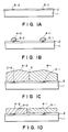
- Fig. 1 is a diagram of the steps for illustration of an example of the crystal formation method of the present invention according to the selective nucleation.
- the substrate on which crystal formation is to be applied is prepared as described below.
- a support 1 which can stand high temperature comprising a high melting glass, quartz, alumina, ceramics, etc. is prepared.
- a non-nucleation surface comprising a material with small nucleation density and a nucleation surface (S NDL ) having greater nucleation density than the non-nucleation surface (S NDS ) and having a sufficiently fine surface area for giving arise to crystal growth with a single nucleus as the originating point to form a monocrystal.
- the material for forming the non-nucleation surface (S NDS ) for example, if a silicon crystal isto be formed, silicon oxide is preferred. However, silicon oxide is not limitative of the present invention, but a material can be used which will cause substantially no nucleation in relationship with the material, the size and the arrangement of the nucleation surface (S NDL ) and the growth conditions.
- the material of the support 1 may be made the material for formation of the non-nucleation surface (S NDS ), and in this case no film comprising the material for non-nucleation surface (S NDS ) may be formed on the support 1.
- a SiO2 film 2 may be deposited according to conventional CVD (Chemical Vapor Deposition) method by use of silane (SiH4) and oxygen (O2).
- the size of the nucleation surface (S NDL ), for permitting a crystal to grow from a single nucleus, has preferably a sufficiently small area, having a diameter generally of several ⁇ m or less and an area of 16 ⁇ m2 or less, more preferably a diameter of 2 ⁇ m or less and an area of 4 ⁇ m2 or less, optimally a diameter of 1 ⁇ m or less and an area of 1 ⁇ m2 or less.
- the material for giving the nucleation surface should preferably be amorphous.
- the method for forming the nucleation surface (S NDL ) there are the method in which it is formed by ion implantation on the non-nucleation surface (S NDS ), the method in which a thin film of a material which will become a nucleation surface (S NDL ) with large nucleation density is formed and then subjected to patterning according to the photolithographic technique, etc.
- the method for forming the nucleation surface (S NDL ) is not limited to these methods.
- the film 2 comprising, for example, SiO2 which gives the non-nucleation surface (S NDS ) is masked to a desired pattern with a photorresist.
- an ion implanter for example, As3 ⁇ ions are implanted into a desired position of the film 2. Namely, As3 ⁇ ions are implanted only into the film 2 through the exposed surface of the film 2 from the mask (Fig. 1 (A)). At the surface where no ion is implanted, the nucleation density (ND S ) of the crystal remains small, and this portion gives the non-nucleation surface (S NDS ).
- the element for the ions to be implanted into the non-nucleation surface when a II-IV group compound crystal is to be grown, there may be included the elements belonging to the group II and the elements belonging to the group VI of the Periodic Table, for example, S, Se, Te, Zn, Cd, etc.
- the elements belonging to the group III and the elements belonging to the group V of Periodic Table for example, N, P, As, Sb, Al, Ga, In, etc.
- the amount of ions implanted may be preferably 1 x 10¹⁵/cm3 or more, more preferably 1 x 10¹⁶/cm3 or more.
- the surface is cleaned and the crystal formation treatment is applied on the substrate.
- the substrate is heated to a predetermined temperature.
- a predetermined temperature 200 to 950 °C may be preferred, but this range is not limitative of the present invention, but an appropriate temperature range may be selected depending on the kind of the crystal to be grown.
- the reaction vessel (crystal growth treatment space) is evacuated internally, a plural number of starting gases are introduced into the reaction vessel, and the starting gases are fed onto the substrate surface alternately so that no general mixing may occur.
- a plural number of starting gases are introduced into the reaction vessel, and the starting gases are fed onto the substrate surface alternately so that no general mixing may occur.
- the concentrations of the starting gases may be alternately changed.
- the pressure range in the reaction vessel during the crystal formation treatment may be preferably 10 ⁇ 1 to 10 Torr when introducing the starting gases, preferably 10 ⁇ 5 to 10 ⁇ 2 Torr when switching over introduction of the starting gases.
- the time for introducing the starting gases into the reaction vessel during the crystal formation treatment may be preferably 5 sec. to 1 min., and the time for evacuating the starting gases preferably 20 sec. to 3 min. It is also preferable that the time for introducing the gases be shorter than the time for evacuating the gases.
- organometallic compounds containing the group II element when the crystal of the group II-VI compound is to be grown, there may be included organometallic compounds containing the group II element and organometallic compounds containing the group VI element or hydrides of the group VI element.
- Specific examples may include dimethylzinc Zn(CH3)2, diethylzinc Zn(C2H5)2, dimethylcadmium Cd(CH3)2, diethylcadmium Cd(C2H5)2, selenium hydride H2Se, dimethylselenium Se(CH3)2, diethylselenium Se(C2H5)2, dimethyltellurium Te(CH3)2, diethyltellurium Te(C2H5)2, hydrogen sulfide H2S, etc.
- organometallic compounds containing the group III element and organometallic compounds containing the group V element or hydrides of the group V element may included as the starting gas.
- Specific examples may include trimethylaluminum Al(CH3)3, triethylaluminum Al(C2H5)3, triisobutylaluminum Al(i-C4H9)3, trimethylgallium Ga(CH3)3, triethylgallium Ga(C2H5)3, trimethylindiumIn(CH3)3, triethylindium In(C2H5)3, tripropylindium In(C3H7)3, tributylindium In(C4H9)3, phosphine PH3, t-butylphosphine t-C4H9PH2, arsine AsH2, trimethylarsine As(CH3)3, triethylarsine As(C2H5)3, diethylarsine (C2H5)2AsH, t-butyl
- the starting gases in introduction of the starting gases into the reaction vessel, they may be diluted with a carrier gas such as H2, He, Ar, etc., if desired.
- a carrier gas such as H2, He, Ar, etc.
- the first point is generation of a plural number of nuclei on the nucleation surface subjected to fine patterning, whereby crystal growth occurs with each of the plural number of nuclei as the originating point of crystal growth, and therefore the crystal grown may become a polycrystal, or in some cases, nucleus is also generated on the non-nucleation surface to cause abnormal nucleus generation phenomenon which disturbs arrangement of the crystal islands which are independent monocrystal regions.
- the second point is occurrence of the defect phenomenon, in which no crystal island grows on the nucleation surface in some of the nucleation surfaces provided in a large number.
- Fig. 2 shows the relationship between the flow rate of HCl, abnormal nucleus generation probability and crystal defect generation probability during crystal growth of Si crystal under the conditions of a substrate temperature of 1030 °C, an amount of SiH2Cl2 introduced of 1.2 slm, an amount of H2 introduced of 100 slm and a pressure of 1 Torr.
- HCl here has the action of etching very fine initial nuclei of Si monocrystals by the reaction according to the reaction formula shown below. Si + nHCl ⁇ SiCln ⁇ + n/2H2 ⁇
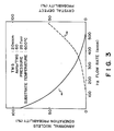
- Fig. 3 shows an example of the result when crystal formation is effected according to the selective nucleation method by introducing simultaneously a plural number of reactive starting gases, showing the relationship between abnormal nucleus generation probability and crystal defect generation probability and H2 flow rate when GaAs crystal was grown under the conditions of a pressure of 20 Torr, a substrate temperature of 600 °C and an introduction amount ratio of AsH3/TMG of 60.
- the present inventor has further studied in view of the various points as described above and consequently invented the crystal formation method of this application which inhibits generation of abnormal nucleus and also reduces crystal defect probability.
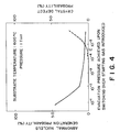
- Fig. 4 shows the relationship of abnormal nucleus generation probability and crystal defect generation probability relative to the pressure within the reaction vessel reached when using a plural number of different starting gases and switching over one of the starting gases with the other starting gas in the crystal formation treatment by the gas phase method.
- Abnormal nucleus generation probability has a critical point at 10 ⁇ 2 Torr, and at the reached pressure of that pressure or lower, the abnormal nucleus generation probability is suppressed at a low level, while at the reached pressure exceeding that pressure, the abnormal nucleus generation probability is increased.
- the crystal defect generation probability has a critical point at 2.5 x 10 ⁇ 5 Torr (see point C), and said crystal defect generation probability is suppressed at a low level at the reached pressure of that pressure or higher, while the crystal defect generation probability is increased at the reached pressure less than that pressure, and at the reached pressure lower than 1 x 10 ⁇ 5 Torr, the above crystal defect generation probability will be increased in excess of the above abnormal nucleus generation probability
- abnormal nucleus generation probability could be suppressed at a low level and also the crystal defect generation probability could be suppressed at a low level according to the crystal growth method of the present invention.
- Fig. 1 the method for forming a GaAs crystal on SiO2 is to be described as an example of the present invention.
- a SiO2 film 2 was deposited to 1000 ⁇ according to the CVD method (chemical vapor deposition method) by use of silane (SiH4) and oxygen (O2) as the startinggases.
- the nucleation density (ND S ) of GaAs on SiO2 is small, and the surface of the SiO2 film gives the non-ncleation surface (S NDS ).
- the surface of the above SiO2 film 2 was masked with a photoresist so that 50 x 50 of 1 ⁇ m square regions were formed.
- ion implanter By use of an ion implanter, As ions were implanted. As ions were implanted only onto the surface exposed (Fig. 1 (A)). The amount implanted at this time was 1 x 10¹⁵/cm2. On the SiO2 surface where no As ion was implanted, the nucleation density (ND S ) remained small as it was, and this portion gave the non-nucleation surface (S NDS ). On the other hand, the regions 3 - 1, 3 - 2, wherein ions were implanted, have greater nucleation density (ND L ) than the non-nucleation surface (S NDS ), and these portions gave the nucleation surface (S NDL ).
- the substrate was subjected to heat treatment in H2 atmosphere at about 900 °C for about 10 minutes to clean the surface.
- TMG trimethyl gallium
- AsH3 arsine
- GaAs crystals 4 - 1, 4 - 2 were formed only on the nucleation surface (S NDL ) 3 - 1, 3 - 2, and no GaAs crystal was formed on the non-nucleation surface (S NDS ), namely on the SiO2 surface where no As ion was implanted.
- GaAs crystals 4 - 1, 4 - 2 became contacted with each other as shown in Fig. 1 (C). At that state, growth was stopped and the surface was polished to effect etching of the grain boundary, whereby GaAs crystals 4 - 1, 4 - 2 were obtained as shown in Fig. 1 (D).
- a SiO2 film 7 was deposited to 1000 ⁇ according to the CVD method by use of SiH4 and O2 as the starting gases.
- SiN x film was deposited to 300 ⁇ according to the CVD method.
- the feeding ratio of SiH4 and NH3 was 2:1, the reaction pressure 0.15 Torr, and the high frequency power was 1.6 x 10 ⁇ 2 W/cm2. Further, the SiN x film was subjected to patterning to 1 ⁇ m square to form nucleation surface (S NDL ) 8 - 1, 8 - 2.
- the substrate thus formed was well washed, it was subjected to heat treatment in H2 atmosphere at about 900 °C for 10 minutes to clean the surface.
- the reaction vessel was internally evacuated to 10 ⁇ 6 Torr, and 5 minutes layer, diethylzinc (DEZn) was introduced with the carrier gas H2 to 1 Torr, followed by evacuation one second later to 10 ⁇ 5 Torr.
- diethylselenium (DESe) together with the carrier gas H2 was introduced to 1 Torr, followed by evacuation one second later to 10 ⁇ 5 Torr.
- H2 and DEZn were again flowed, and the above-described operations were repeated to grow ZnSe crystals.
- ZnSe monocrystals 9 - 1, 9 - 2 were grown originating from the nuclei formed on the nucleation surfaces (S NDL ) 8 - 1, 8 - 2 formed of SiN x , and crystals were grown even to the non-nucleation surface (S NDS ), namely on the surface of SiO2 film 7.
- S NDS non-nucleation surface
- ZnSe crystals 9A - 1, 9A - 2 were grown larger even until they came into contact with each other to form a polycrystal.
- the surface of the polycrystal formed was polished to effect etching of the grain boundary 10, whereby ZnSe monocrystals 9B - 1, 9B - 2 as shown in Fig. 5 (D) were obtained. Also in this Example similarly as in Example 1, abnormal nucleus generation probability and crystal defect probability were suppressed at low levels.
Landscapes
- Chemical & Material Sciences (AREA)
- Chemical Kinetics & Catalysis (AREA)
- General Chemical & Material Sciences (AREA)
- Engineering & Computer Science (AREA)
- Crystallography & Structural Chemistry (AREA)
- Materials Engineering (AREA)
- Metallurgy (AREA)
- Organic Chemistry (AREA)
- Recrystallisation Techniques (AREA)
Applications Claiming Priority (2)
| Application Number | Priority Date | Filing Date | Title |
|---|---|---|---|
| JP209462/87 | 1987-08-24 | ||
| JP20946287 | 1987-08-24 |
Publications (1)
| Publication Number | Publication Date |
|---|---|
| EP0312202A1 true EP0312202A1 (de) | 1989-04-19 |
Family
ID=16573271
Family Applications (1)
| Application Number | Title | Priority Date | Filing Date |
|---|---|---|---|
| EP88307859A Withdrawn EP0312202A1 (de) | 1987-08-24 | 1988-08-24 | Verfahren zur Herstellung eines Kristalls |
Country Status (2)
| Country | Link |
|---|---|
| EP (1) | EP0312202A1 (de) |
| AU (1) | AU615469B2 (de) |
Cited By (1)
| Publication number | Priority date | Publication date | Assignee | Title |
|---|---|---|---|---|
| CN120187166A (zh) * | 2025-05-22 | 2025-06-20 | 南昌凯迅光电股份有限公司 | 一种改善抗静电能力的led外延片及其制备方法 |
Citations (5)
| Publication number | Priority date | Publication date | Assignee | Title |
|---|---|---|---|---|
| GB2162862A (en) * | 1984-07-26 | 1986-02-12 | Japan Res Dev Corp | Process for forming monocrystalline thin film of compound semiconductor |
| FR2588416A1 (fr) * | 1985-10-07 | 1987-04-10 | Canon Kk | Procede de formation selective d'un film depose |
| US4657603A (en) * | 1984-10-10 | 1987-04-14 | Siemens Aktiengesellschaft | Method for the manufacture of gallium arsenide thin film solar cells |
| EP0241204A2 (de) * | 1986-03-31 | 1987-10-14 | Canon Kabushiki Kaisha | Herstellungsverfahren einer niedergeschlagenen Kristallschicht |
| EP0244081A1 (de) * | 1986-03-28 | 1987-11-04 | Canon Kabushiki Kaisha | Verfahren zur Herstellung eines Kristalls und Kristallkörper, die nach diesem Verfahren hergestellt werden |
-
1988
- 1988-08-24 AU AU21501/88A patent/AU615469B2/en not_active Ceased
- 1988-08-24 EP EP88307859A patent/EP0312202A1/de not_active Withdrawn
Patent Citations (5)
| Publication number | Priority date | Publication date | Assignee | Title |
|---|---|---|---|---|
| GB2162862A (en) * | 1984-07-26 | 1986-02-12 | Japan Res Dev Corp | Process for forming monocrystalline thin film of compound semiconductor |
| US4657603A (en) * | 1984-10-10 | 1987-04-14 | Siemens Aktiengesellschaft | Method for the manufacture of gallium arsenide thin film solar cells |
| FR2588416A1 (fr) * | 1985-10-07 | 1987-04-10 | Canon Kk | Procede de formation selective d'un film depose |
| EP0244081A1 (de) * | 1986-03-28 | 1987-11-04 | Canon Kabushiki Kaisha | Verfahren zur Herstellung eines Kristalls und Kristallkörper, die nach diesem Verfahren hergestellt werden |
| EP0241204A2 (de) * | 1986-03-31 | 1987-10-14 | Canon Kabushiki Kaisha | Herstellungsverfahren einer niedergeschlagenen Kristallschicht |
Non-Patent Citations (3)
| Title |
|---|
| APPLIED PHYSICS LETTERS, vol. 47, no. 9, 1st November 1985, pages 955-957, American Institute of Physics, Woodbury, New York, US; S FUJITA et al.: "Blue luminescence of a ZnSe-ZnSo.1Seo.9 strained-layer superlattice on a GaAs substrate grown by low-pressure organometallic vapor phase epitaxy" * |
| BRITISH JOURNAL OF APPLIED PHYSICS, vol. 18, no. 10, October 1967, pages 1357-1382, GB; J.D. FILBY et al.: "Single-crystal films of silicon on insulators" * |
| JOURNAL OF APPLIED PHYSICS, vol. 58, no. 7, 1st October 1985, pages 2767-2769, American Institute of Physics, Woodbury, New York, US; S OKU et al.: "InP crystal growth on planar SiO2 substrates" * |
Cited By (1)
| Publication number | Priority date | Publication date | Assignee | Title |
|---|---|---|---|---|
| CN120187166A (zh) * | 2025-05-22 | 2025-06-20 | 南昌凯迅光电股份有限公司 | 一种改善抗静电能力的led外延片及其制备方法 |
Also Published As
| Publication number | Publication date |
|---|---|
| AU2150188A (en) | 1989-03-02 |
| AU615469B2 (en) | 1991-10-03 |
Similar Documents
| Publication | Publication Date | Title |
|---|---|---|
| EP0179138B1 (de) | Ein verfahren zur herstellung einer verbindungshalbleiterstruktur | |
| US5268327A (en) | Epitaxial compositions | |
| US4910167A (en) | III-V Semiconductor growth initiation on silicon using TMG and TEG | |
| JPH01225114A (ja) | 半導体薄膜の製造方法 | |
| CA1086431A (en) | Etching of iii-v semiconductor materials in the preparation of heterodiodes | |
| JPH06132236A (ja) | 半導体装置の製造方法 | |
| US4835116A (en) | Annealing method for III-V deposition | |
| US4900372A (en) | III-V on Si heterostructure using a thermal strain layer | |
| EP0241204B1 (de) | Herstellungsverfahren einer niedergeschlagenen Kristallschicht | |
| US5718761A (en) | Method of forming crystalline compound semiconductor film | |
| US5296087A (en) | Crystal formation method | |
| EP0288166B1 (de) | Verfahren zur selektiven Herstellung von III-V Halbleiterschichten | |
| EP0312202A1 (de) | Verfahren zur Herstellung eines Kristalls | |
| US5334864A (en) | Process for selective formation of II-VI group compound film | |
| US5100691A (en) | Process for selective formation of ii-vi group compound flim | |
| Bertone | Atomic layer epitaxy of InP | |
| JPH03215390A (ja) | 化合物結晶のエピタキシャル成長におけるドーピング方法 | |
| JP2528912B2 (ja) | 半導体成長装置 | |
| JP2569141B2 (ja) | 結晶形成方法 | |
| JP2569140B2 (ja) | 結晶性化合物半導体膜の形成方法 | |
| JP2736417B2 (ja) | 半導体素子の製法 | |
| JP2952831B2 (ja) | 半導体装置の製造方法 | |
| JP2668236B2 (ja) | 半導体素子の製法 | |
| JPH0419700B2 (de) | ||
| EP0289117B1 (de) | Verfahren zur Herstellung von Kristallen auf einem Substrat |
Legal Events
| Date | Code | Title | Description |
|---|---|---|---|
| PUAI | Public reference made under article 153(3) epc to a published international application that has entered the european phase |
Free format text: ORIGINAL CODE: 0009012 |
|
| AK | Designated contracting states |
Kind code of ref document: A1 Designated state(s): DE FR GB IT NL |
|
| 17P | Request for examination filed |
Effective date: 19890911 |
|
| 17Q | First examination report despatched |
Effective date: 19910909 |
|
| STAA | Information on the status of an ep patent application or granted ep patent |
Free format text: STATUS: THE APPLICATION IS DEEMED TO BE WITHDRAWN |
|
| 18D | Application deemed to be withdrawn |
Effective date: 19980222 |