EP0312214B1 - Datensignal-Wiedergabegerät - Google Patents
Datensignal-Wiedergabegerät Download PDFInfo
- Publication number
- EP0312214B1 EP0312214B1 EP88308755A EP88308755A EP0312214B1 EP 0312214 B1 EP0312214 B1 EP 0312214B1 EP 88308755 A EP88308755 A EP 88308755A EP 88308755 A EP88308755 A EP 88308755A EP 0312214 B1 EP0312214 B1 EP 0312214B1
- Authority
- EP
- European Patent Office
- Prior art keywords
- signal
- reproduction
- order differential
- window
- detecting
- Prior art date
- Legal status (The legal status is an assumption and is not a legal conclusion. Google has not performed a legal analysis and makes no representation as to the accuracy of the status listed.)
- Expired - Lifetime
Links
- 230000000052 comparative effect Effects 0.000 claims description 32
- 230000003111 delayed effect Effects 0.000 claims description 3
- 239000010409 thin film Substances 0.000 description 8
- 230000003287 optical effect Effects 0.000 description 6
- 238000010586 diagram Methods 0.000 description 5
- 230000000694 effects Effects 0.000 description 3
- 239000010408 film Substances 0.000 description 3
- 230000010287 polarization Effects 0.000 description 3
- 238000001514 detection method Methods 0.000 description 2
- 230000001678 irradiating effect Effects 0.000 description 2
- 230000005415 magnetization Effects 0.000 description 2
- 230000005374 Kerr effect Effects 0.000 description 1
- 239000003990 capacitor Substances 0.000 description 1
- 238000010276 construction Methods 0.000 description 1
- 230000003247 decreasing effect Effects 0.000 description 1
- 230000000873 masking effect Effects 0.000 description 1
- 238000000034 method Methods 0.000 description 1
- 230000001105 regulatory effect Effects 0.000 description 1
- 230000002441 reversible effect Effects 0.000 description 1
Images


Classifications
-
- G—PHYSICS
- G11—INFORMATION STORAGE
- G11B—INFORMATION STORAGE BASED ON RELATIVE MOVEMENT BETWEEN RECORD CARRIER AND TRANSDUCER
- G11B20/00—Signal processing not specific to the method of recording or reproducing; Circuits therefor
- G11B20/10—Digital recording or reproducing
- G11B20/10009—Improvement or modification of read or write signals
Definitions
- the present invention relates to a digital signal reproduction apparatus for reproducing digital signals recorded on a recording medium such as a magnetooptical disc.
- a magneto-optical disc has a magnetic thin film on its surface as a recording medium with magnetic anisotropy such that the axis of easy magnetization is oriented perpendicularly to the surface of the film. Data is recorded or reproduced onto or from the magnetic thin film by irradiating it with a laser beam condensed into a diameter of about 1 m.
- a strong laser beam is irradiated onto the thin film. This raises the temperature of the irradiated spot locally to decrease the coercive force in the vicinity. Accordingly, when a reverse biased magnetic field is applied to the spot, from outside the magnetization of the spot is inverted. Accordingly, if the strength of the laser beam or the direction of the biased magnetic field is controlled according to the data signals to be recorded, data is recorded onto the thin film as dots having the diameter of the laser beam.
- a substantially similar method is employed to erase the recorded signals.
- the magnetic thin film is irradiated with a weaker laser beam than the recording beam.
- the laser beam irradiating spot on the film is linearly polarized with a polarization plane inclined according to the magnetized state of the spot by the magneto-optical effect (Faraday effect or Kerr effect) and is reflected from the surface of the film.
- the recorded data signal can be reproduced by detecting the inclination of the polarization plane by converting it into an electrical signal by an optical detector through an analyzer.
- Fig. 3 is a schematic diagram of the reproduction system for the magneto-optical disc.
- the beam When a laser beam generated by an optical head 1 irradiates the thin film of the magneto-optical disc 2, the beam is reflected toward the optical head 1 and converted into a reproduction signal corresponding to the inclination of the polarization plane.
- the reproduction signal is transmitted to a data detecting circuit 3 and the recorded data signal is output as a reproduction data signal.
- the conventional data detecting circuit 3 used for the above reproduction system will be described referring to Figs. 4 and 5.
- a recording data signal S11 comprising a series of "0's" and "1's”
- the reproduction signal S12 generated from the recording data signal S11 has a wave form in which each peak corresponds to a "1" of the recording data signal S11.
- the reproduction signal S12 is input respectively to a differential circuit 21, a comparative voltage generating circuit 22, and a comparator 23 of the data detection circuit 3, as shown in Fig. 4.
- the differential circuit 21 differentiates the reproduction signal S12 and outputs a differential signal S13.
- the differential signal S13 has a wave form having zero-cross points corresponding to individual maximum and minimum values of the reproduction signal S12 as shown in Fig. 5.
- the differential signal S13 is input into a comparator 24.
- the comparator 24 compares the differential signal with a 0 V level and outputs a differential digital signal S15.
- the trailing edge of pulses of the differential digital signals S15 correspond to zero-cross points of the differential signal S13 as it changes from a positive value to a negative value. It therefore corresponds to each peak point (maximum point in the conventional example) of the reproduction signal S12, namely, it represents a position corresponding to "1" of the recorded recording data signal S11. Therefore, if the trailing edge is detected by a trailing edge detecting circuit 25, a peak detecting signal corresponding to "1" of the recording data signal S11 is obtained.
- the differential signal S13 is also held at the zero-crossing level for a relatively long time as indicated by a circle E of Fig. 5. This is apt to cause noise in the differential digital signal S15 and the peak detecting signal S17. It, therefore, becomes necessary to remove noise in the peak detecting signal S17 in order to pick up only pulses representing peaks of the reproduction signal S12.
- the comparative voltage generating circuit 22 generates another comparative voltage S12' based on the reproduction signal S12, the comparative voltage S12' providing a threshold voltage for detecting the vicinity of each peak of the reproduction signal S12.
- the comparator 23 compares the reproduction signal S12 with the comparative voltage S12', and outputs a window signal S16 that provides a signal indicative of the vicinity of the peak of the reproduction signal S12.
- the peak detecting signal S17 and the window signal S16 are then input to an AND gate 26 the output of which masks unwanted noise found in the peak detecting signal S17.
- the level margin between the reproduction signal S12 and the comparative voltage S12' compared at the comparator 23 is relatively low. Accordingly, when there is a fluctuation in the amplitude of the reproduction signal S12 a corresponding error may be created in the output window signal S16. Furthermore, in an optical memory apparatus such as the above-mentioned magnetooptical disc etc., the reproduction signal S12 includes low frequency components, causing the level margin to be further decreased creating a greater likelihood of error in the window signal S16. For example, when a drop-out is caused in the reproduction signal S12 as indicated by a circle F of Fig. 5, the window signal S16 is not opened. As a consequence, the detecting pulse does not appear in the reproduction data signal S18 although a pulse representing the peak appears in the peak detecting signal S17.
- US 4,764,916 describes a reading circuit for an optical disc apparatus according to the preamble of claim 1 and another embodiment that utilises window signals generated from first and second differential signals to eliminate noise in the reproduction signal.
- JP 59-79409 relates to restoration of a transmitted original signal in a field somewhat different to that of the present invention. It describes apparatus that utilises a window signal derived from first and third differentials of the input signal and a window signal derived from the second differential to restore a transmitted signal.
- An object of the present invention is to alleviate at least some of the aforementioned problems.
- a digital signal reproduction apparatus for reproducing a digital data signal in response to a reproduction signal reproduced from a recording medium, comprising a comparative voltage generator for generating a threshold voltage, first comparing means for comparing the reproduction signal with the threshold voltage and outputting a first window signal representing the comparison result thereof, first differential means for differentiating the reproduction signal, and outputting a first order differential signal, and peak detecting means for detecting a zero-crossing point of the first order differential signal, and outputting a peak detecting signal, characterised in that the comparative voltage generator is operable to generate said threshold voltage on the basis of the reproduction signal so as to have a level set to be slightly higher than the minimum level of the reproduction signal and in that the digital signal reproduction apparatus further comprises: second order differential means for differentiating the first order differential signal and outputting a second order differential signal; second comparing means for comparing the second order differential signal with a predetermined level and outputting a second window signal representing the comparison result thereof; and gate means for gating the peak
- the comparative voltage is to detect the amplitude of the reproduction signal, and can be obtained from the direct current component by a comparative voltage generating circuit or may be obtained from a constant voltage source regulated by a power supply unit.
- the first comparing means provides the first window signal by comparing the reproduction signal with the comparative voltage and outputting the difference. Since the comparative voltage is used to remove noise in the peak detecting signal by generating the first window signal, a relatively large level margin can be set compared to that possible in conventional comparative voltage generating circuits.
- the second window signal used for gating the peak detecting signal can be generated by a second order differential means and a second comparing means.
- the second order differential signal When the first order differential signal is differentiated by the second differential means, the second order differential signal has a wave form with maxima and minima corresponding to zero-crossing points of the first order differential signal.
- the second order differential signal is a signal representative of the change in the amplitude of the first differential signal, the second differential signal is not affected to any great extent by fluctuations in amplitude or low frequency components.
- the second window signal representing the zero-crossing point of the first differential signal can be obtained by comparing the second order differential signal with a predetermined value. If the peak points of the reproduction signal to be detected are maxima, the zero-crossing points at which the first order differential signal changes from positive to negative correspond to the maxima of the reproduction signal.
- the predetermined value is set at a ground level, noise may be caused in the second window signal by the effect of the unstable portions of the first differential signal. However such noise is removed by ANDing with the first window signal.
- the first window signal is only used for removing noise which may be generated in the peak detecting signal, a relatively large level of margin can be set for the comparative voltage for the first comparing means. Noises due to amplitude fluctuation, low frequency components, and drop-out, in the reproduction signal is thereby removed.
- the second window signal is generated from the second order differential signal, the second window signal is also not affected by amplitude fluctuation and low frequency components, and the pulses of the second window signal are accurately output even if there are some drop-outs present in the reproduction signal. Accordingly, since the peak detecting signal is gated with the first and second window signals, noise is dependably removed and only pulses corresponding to respective peaks of the reproduction signal are passed by the gate means.
- a reproduction signal reproduced from a recording medium has amplitude fluctuations low frequency components or drop-out, the correct reproduction data signal can be obtained with certainty.
- a reproduction signal reproduced from a recording medium such as a magnetooptical disc often includes low frequency components, however, an accurate reproduction data signal can be obtained unaffected by low frequency components.
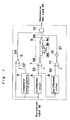
- an optical reading head 1 reads out data recorded on a magneto-optical disc 2 and outputs a reproduction signal S2 to a data detecting circuit 3.
- Fig. 1 is a schematic diagram of the data detecting circuit 3.
- the reproduction signal S2 is input respectively to input terminals of a comparative voltage generating circuit 4, a differential circuit 6, and a non-inverted input terminal of a comparator 5.
- the differential circuit 6 differentiates the reproduction signal and outputs a first order differential signal S3 respectively to a non-inverted input terminal of a comparator 7 and an input terminal of another differential circuit 8.
- the inverted input terminal of the comparator 7 is connected to ground.
- the comparator 7 compares the first order differential signal S3 with a zero voltage level to output a differential digital signal S6 to an input terminal of a trailing edge detecting circuit 9.
- the trailing edge detecting circuit 9 comprises a time constant circuit 9a having a resistor R and a capacitor C, an inverter 9b, and a NOR gate 9c. In the trailing edge detecting circuit 9, the differential digital signal S6 is delayed by the time constant circuit 9a, inverted by the inverter 9b.
- the inverted signal is then input to the input terminal of the NOR gate 9c.
- the differential digital signal S6 is input directly to another input terminal of NOR gate 9c.
- the NOR gate 9c outputs a peak detecting signal S8 representing the trailing edge of each pulse of the differential digital signal S6 to an input terminal of an AND gate 10.
- the composition of the trailing edge detecting circuit 9 is substantially the same as conventional trailing edge detecting circuits.
- the comparative voltage generating circuit 4 comprises a low pass filter or an envelope detector and generates a comparative voltage S2' based on the reproduction signal S2.
- the comparative voltage S2' represents a threshold voltage for determining that the reproduction signal S2 is not close to its minimum level.
- the comparative voltage generating circuit 4 may be constructed to output a constant voltage signal from a constant voltage source independently of the reproduction signal S2.
- the output signal S2' from the comparative voltage generating circuit 4 is input into the inverted input terminal of the comparator 5.
- the comparator 5 compares the reproduction signal S2 with the comparative voltage S2' and outputs a first window digital signal S5. This is then input to the second input terminal of the AND gate 10.
- the first window signal S5 is used to remove noise from the peak detecting signal S8 by masking voltages close to the minimum of the reproduction signal. Since the first window signal S5 masks only signals in the vicinity of the minimum voltage of the reproduction signal S2, the comparative voltage S2' can be set to provide a relatively large level margin.
- the comparative voltage generating circuit 4 and the comparator 5 can then output accurately the first window signal S5 pulses to open the AND gate 10 unaffected by amplitude fluctuation, low frequency components or drop-out.
- Another differential circuit 8 differentiates the first order differential signal S3 and provides a second order differential signal S4 to a non-inverted input terminal of a comparator 11.
- An inverted input terminal of the comparator 11 is connected to ground.
- the comparator 11 compares the second order differential signal S4 with a zero voltage in order to output a digital signal S7 to the third input terminal of the AND gate 10 through an inverter 12.
- the inverter 12 outputs an inverted signal of the output of the comparator 11 as a second window signal.
- the peak detecting signal S8 is gated with the first and second window signals by the AND gate 10.
- the AND gate 10 outputs the reproduction data signal S9.
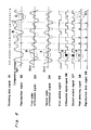
- the reproduction signal S2 is output as a wave form having peaks corresponding to "1's” and troughs corresponding to "0's".
- the differentiating circuit 6 differentiates the reproduction signal S2 and outputs the first order differential signal S3.
- the first order differential signal S3 has a wave form having zero-crossing points corresponding to maxima and minima of the reproduction signal S2.
- the first order differential signal S3 is compared with the 0 V level by the comparator 7, and a differential signal S6 is output.
- the trailing edge of each pulse of the differential digital signal S6 corresponds to a zero-crossing point travelling from positive to negative of the first order differential signal S3.
- the trailing edge of each pulse of the differential digital signal S6 corresponds to a "1" of the recorded data signal S1.
- a peak detecting signal S8 can, therefore, obtain a pulse corresponding to "1" by detecting trailing edges of the differential digital signal S6 with the trailing edge detecting circuit 9.
- the peak detecting signal S8 includes noise created by unstable portions of the first order differential signal as indicated by a circle A in Fig. 2 and/or by errors due to drop-out of the reproduction signal S2 such as those indicated by a circle D in Fig. 2. This noise and such errors can be eliminated as explained below.
- the reproduction signal S2 is compared with the comparative voltage S2' by the comparator 5 to generate the first window signal S5. Since the comparative voltage S2' is set at a voltage slightly larger than the minimum of the reproduction signal S2, a relatively large level margin can be set. Therefore, although drop-outs in the reproduction signal S2 such as those indicated by the circles B and C, the pulses of the reproduction data signal S9 can be accurately output by opening the window gate 10 without being affected by the drop-outs. Further, at the minima of the reproduction signal S2 where noise is likely to be generated in the peak detecting signal S8 and at a maxima lower than expected due to drop-out of the reproduction signal S2 wherein a detecting error may be caused in the peak detecting signal S9, the gate 10 is shut.
- the first order differential signal S3 is differentiated by the differential circuit 8.
- the second order differential signal S4 has a wave form showing only changes in the amplitude of the first order differential signal S3, the second order differential signal S4 is not substantially effected by the amplitude fluctuation and the low frequency components in the reproduction signal S2.
- the second differential signal S4 is compared with a zero level voltage by the comparator 11, is inverted by the invertor 12, and output as the second window signal S7.
- the output of the comparator 11 is a signal that indicates the vicinity of the zero-crossing point when the first order differential signal varies from positive to negative. This corresponds to maxima of the reproduction signal S2.
- the comparative voltage of the comparator 11 is set at a slightly small negative voltage, noise in the second window signal S7 such as that as shown in the circle A, can be removed in advance.
- the second window signal S7 is not effected by amplitude fluctuations or low frequency components.
- the correct pulse corresponding to maxima of the reproduction signal S2 is output to open the window gate 10 even if drop-outs are caused in the reproduction signal S2 as indicated by circles B and C.
- the window is opened by the second window signal S7. In this case, a possible error in detecting the peak detecting signal S8 is avoided by the first window signal S5.
- the comparative voltage of the comparator 11 is set at the zero voltage level in the construction of Fig. 1, noise such as that as shown in the circle A may be generated in the second window signal S7 as well as in the peak detecting signal S8, however, the noise will be removed by the first window signal S5.
- the peak detecting signal S8 is gated by the AND gate 10 in accordance with the first window signal S5 and the second window signal S7.
- the AND gate 10 outputs the reproduction data signal S9.
- the data detecting circuit 3 can gate the peak detecting signal S8 with both the first and the second window signals, the detecting error of the peak point due to noise and/or drop-outs can be reliably avoided and the reproduction data signal S9 obtained unaffected by amplitude fluctuations, low frequency components and drop-out in reproduction signal.
Landscapes
- Engineering & Computer Science (AREA)
- Signal Processing (AREA)
- Signal Processing For Digital Recording And Reproducing (AREA)
Claims (6)
- Einrichtung zur Wiedergabe von Digitalsignalen (S9) in Abhängigkeit eines von einem Aufzeichnungsmedium abgreifbaren Reproduktionssignals (S2) mit einem Vergleichsspannungsgenerator (4), der eine Schwellenspannung (S2') liefert, einer ersten Vergleichseinrichtung (5), die das Reproduktionssignal (S2) gegen die Schwellenspannung (S2') vergleicht und ein dem Vergleichsergebnis entsprechendes erstes Fenstersignal (S5) ausgibt, einer ersten Differenziereinrichtung (6), die das Reproduktionssignal (S2) differenziert und ein Differenzsignal (S3) erster Ordnung ausgibt, einer Spitzenwert-Abtasteinrichtung (6, 7, 9) zum Ermitteln eines Nulldurchgangs beim Differenzsignal (S3) erster Ordnung sowie zur Ausgabe eines Spitzenwert-Abtastsignals (S8), dadurch gekennzeichnet, daß der Vergleichsspannungsgenerator (4) die Schwellenspannung (S2') auf der Grundlage des Reproduktionssignals (S2) auf einen Pegel einstellt, der etwas über dem Minimumpegel des Reproduktionssignals (S2) liegt, und weiterhin dadurch gekennzeichnet, daß die Digitalsignal-Wiedergabeeinrichtung folgende Baugruppen aufweist:
eine zweite Differenziereinrichtung (8), die das Differenzsignal (S3) erster Ordnung differenziert und ein Differenzsignal (S4) zweiter Ordnung abgibt;
eine zweite Vergleichseinrichtung (11), welche das Differenzsignal (S4) zweiter Ordnung mit einem festgelegten Wert vergleicht und ein dem Vergleichsergebnis entsprechendes zweites Fenstersignal (S7) liefert; sowie
eine Torschaltung (10) zum Verknüpfen des Spitzenwert-Abtastsignals (S8) mit dem ersten und zweiten Fenstersignal (S5, S7) sowie zum Ausgeben des reproduzierten Digitaldatensignals. - Digitalsignal-Wiedergabeeinrichtung nach Anspruch 1, bei welcher die Spitzenwert-Abtasteinrichtung (6, 7, 9) einen Komparator (7) aufweist, der das Differenzsignal (S3) erster Ordnung gegen einen Nullpegel vergleicht, und bei der eine Vorderflanken-Abtastschaltung (9) vorhanden ist, die jede Vorderflanke im Ausgangssignal des Komparators detektiert.
- Digitalsignal-Wiedergabeeinrichtung nach Anspruch 2, bei der die Vorderflanken-Abtastschaltung (9) einen Zeitkonstantenkreis (9a) aufweist, der das vom Komparator (7) abgegebene Signal (S6) verzögert, und bei der weiterhin ein Inverter (9b) zum Invertieren des verzögerten Signals sowie ein NOR-Glied (9c) vorhanden ist, welches das verzögerte Signal mit dem invertierten Signal verknüpft und ausgangsseitig ein Vorderflankenspitzenwert-Abtastsignal (S8) abgibt.
- Digitalsignal-Wiedergabeeinrichtung nach einem der Ansprüche 1 bis 3, bei der der Vergleichsspannungsgenerator ein Tiefpaßfilter aufweist.
- Digitalsignal-Wiedergabeeinrichtung nach einem der Ansprüche 1 bis 3, bei der der Vergleichsspannungsgenerator einen Hüllkurvendetektor aufweist.
- Digitalsignal-Wiedergabeeinrichtung nach einem der vorstehenden Ansprüche, bei welcher der Vorgabepegel ein relativ kleiner negativer Spannungswert ist.
Applications Claiming Priority (4)
| Application Number | Priority Date | Filing Date | Title |
|---|---|---|---|
| JP236757/87 | 1987-09-21 | ||
| JP23675787A JPS6479973A (en) | 1987-09-21 | 1987-09-21 | Digital signal reproducing device |
| JP270607/87 | 1987-10-27 | ||
| JP27060787A JPH01112569A (ja) | 1987-10-27 | 1987-10-27 | デジタル信号再生装置 |
Publications (2)
| Publication Number | Publication Date |
|---|---|
| EP0312214A1 EP0312214A1 (de) | 1989-04-19 |
| EP0312214B1 true EP0312214B1 (de) | 1992-08-12 |
Family
ID=26532841
Family Applications (1)
| Application Number | Title | Priority Date | Filing Date |
|---|---|---|---|
| EP88308755A Expired - Lifetime EP0312214B1 (de) | 1987-09-21 | 1988-09-21 | Datensignal-Wiedergabegerät |
Country Status (4)
| Country | Link |
|---|---|
| US (2) | US4954903A (de) |
| EP (1) | EP0312214B1 (de) |
| CA (1) | CA1322594C (de) |
| DE (1) | DE3873678T2 (de) |
Families Citing this family (9)
| Publication number | Priority date | Publication date | Assignee | Title |
|---|---|---|---|---|
| US4954903A (en) * | 1987-09-21 | 1990-09-04 | Sharp Kabushiki Kaisha | Digital signal reproduction apparatus for reading magneto-optical disks |
| JPH0814936B2 (ja) * | 1990-04-06 | 1996-02-14 | シャープ株式会社 | 情報再生回路 |
| JPH04209323A (ja) * | 1990-12-07 | 1992-07-30 | Olympus Optical Co Ltd | 光学的情報記録/再生装置の読取り信号処理回路 |
| US5223989A (en) * | 1991-04-25 | 1993-06-29 | Storage Technology Corporation | Data detection circuit having a pulse shape and amplitude measuring sampling detector |
| DE69220015T2 (de) * | 1991-12-27 | 1997-09-25 | Matsushita Electric Ind Co Ltd | Optische Platten Lesegerät |
| US5424883A (en) * | 1992-06-01 | 1995-06-13 | Eastman Kodak Company | Signal channel equalizer and method of making same |
| DE4226777A1 (de) * | 1992-08-13 | 1994-02-17 | Thomson Brandt Gmbh | Rauschanteilverringerung im Datensignal und optische Abtastvorrichtung |
| JPH09128904A (ja) * | 1995-11-01 | 1997-05-16 | Canon Inc | 情報再生装置 |
| KR100858313B1 (ko) * | 2007-01-05 | 2008-09-11 | (주)위더스비젼 | 제로 크로스 검출기 및 오디오 장치의 뮤트 신호 발생기 |
Citations (1)
| Publication number | Priority date | Publication date | Assignee | Title |
|---|---|---|---|---|
| US4764916A (en) * | 1985-03-05 | 1988-08-16 | Nec Corporation | Reading circuit for an optical disk apparatus |
Family Cites Families (10)
| Publication number | Priority date | Publication date | Assignee | Title |
|---|---|---|---|---|
| US3252099A (en) * | 1963-05-27 | 1966-05-17 | Ibm | Waveform shaping system for slimming filter control and symmetrizing |
| US4475183A (en) * | 1981-10-26 | 1984-10-02 | Eastman Kodak Company | Optical disk retrieval methods, media and systems employing digital data of high fractional bandwidth |
| US4480276A (en) * | 1982-07-28 | 1984-10-30 | Hewlett-Packard Company | Apparatus for peak detection in magnetic recording |
| JPS5979409A (ja) * | 1982-10-29 | 1984-05-08 | Sony Corp | デイジタル信号復元方式 |
| JPS61120380A (ja) * | 1984-11-16 | 1986-06-07 | Sony Corp | デジタル信号処理回路 |
| JP2641421B2 (ja) * | 1985-03-22 | 1997-08-13 | 株式会社日立製作所 | 光学的検出方法、光学的情報再生装置、及び信号検出回路 |
| EP0220023B1 (de) * | 1985-10-08 | 1993-07-07 | Sharp Kabushiki Kaisha | Magnetooptische Speichervorrichtung |
| US4686586A (en) * | 1986-01-21 | 1987-08-11 | Oki America, Inc. | Read back circuit for recovering data from magnetic storage medium |
| US4954903A (en) * | 1987-09-21 | 1990-09-04 | Sharp Kabushiki Kaisha | Digital signal reproduction apparatus for reading magneto-optical disks |
| JPH01284876A (ja) * | 1988-05-12 | 1989-11-16 | Ricoh Co Ltd | 記録装置 |
-
1988
- 1988-09-19 US US07/245,771 patent/US4954903A/en not_active Expired - Fee Related
- 1988-09-19 CA CA000577830A patent/CA1322594C/en not_active Expired - Fee Related
- 1988-09-21 EP EP88308755A patent/EP0312214B1/de not_active Expired - Lifetime
- 1988-09-21 DE DE8888308755T patent/DE3873678T2/de not_active Expired - Fee Related
-
1990
- 1990-03-26 US US07/498,710 patent/US5166838A/en not_active Expired - Fee Related
Patent Citations (1)
| Publication number | Priority date | Publication date | Assignee | Title |
|---|---|---|---|---|
| US4764916A (en) * | 1985-03-05 | 1988-08-16 | Nec Corporation | Reading circuit for an optical disk apparatus |
Also Published As
| Publication number | Publication date |
|---|---|
| DE3873678T2 (de) | 1993-03-25 |
| EP0312214A1 (de) | 1989-04-19 |
| CA1322594C (en) | 1993-09-28 |
| US4954903A (en) | 1990-09-04 |
| US5166838A (en) | 1992-11-24 |
| DE3873678D1 (de) | 1992-09-17 |
Similar Documents
| Publication | Publication Date | Title |
|---|---|---|
| EP0430811B1 (de) | Optomagnetisches Signalwiedergabegerät | |
| EP0232867A1 (de) | Optisches Speichergerät | |
| CA2025121C (en) | Information recording and reproducing device | |
| EP0312214B1 (de) | Datensignal-Wiedergabegerät | |
| US4706236A (en) | Slice level corrector | |
| US5661713A (en) | Optical information reproducing apparatus with a threshold level generator to eliminate DC level fluctuation | |
| US4525822A (en) | Optical data recordation and reproduction system | |
| EP0450622B1 (de) | Daten-Wiedergabeschaltung | |
| US4785252A (en) | Waveform processing circuit | |
| JPH0677371B2 (ja) | 記憶情報読出回路 | |
| JP2948016B2 (ja) | 情報記録再生方法 | |
| JPH01112569A (ja) | デジタル信号再生装置 | |
| EP0325488A1 (de) | Analogsignalschaltvorrichtung für ein optisches Speichergerät | |
| JPH0474780B2 (de) | ||
| JP2817688B2 (ja) | 光ディスク記録パワー制御装置 | |
| JPH04162237A (ja) | 情報再生装置 | |
| KR930011378B1 (ko) | 3진데이타의 기록재생방법 | |
| JPH0765379A (ja) | 情報記録装置 | |
| JPH0589476A (ja) | 情報再生装置 | |
| JPS626408A (ja) | ピ−ク検出回路 | |
| JPH0559507B2 (de) | ||
| JPH05225634A (ja) | 光磁気ディスク再生方式 | |
| JPH0519206B2 (de) | ||
| JP2002032958A (ja) | 再生信号処理回路 | |
| JPS62185277A (ja) | 光メモリ装置の信号検出回路 |
Legal Events
| Date | Code | Title | Description |
|---|---|---|---|
| PUAI | Public reference made under article 153(3) epc to a published international application that has entered the european phase |
Free format text: ORIGINAL CODE: 0009012 |
|
| 17P | Request for examination filed |
Effective date: 19881014 |
|
| AK | Designated contracting states |
Kind code of ref document: A1 Designated state(s): DE FR GB IT NL |
|
| 17Q | First examination report despatched |
Effective date: 19900918 |
|
| GRAA | (expected) grant |
Free format text: ORIGINAL CODE: 0009210 |
|
| AK | Designated contracting states |
Kind code of ref document: B1 Designated state(s): DE FR GB IT NL |
|
| REF | Corresponds to: |
Ref document number: 3873678 Country of ref document: DE Date of ref document: 19920917 |
|
| ET | Fr: translation filed | ||
| ITF | It: translation for a ep patent filed | ||
| PLBE | No opposition filed within time limit |
Free format text: ORIGINAL CODE: 0009261 |
|
| STAA | Information on the status of an ep patent application or granted ep patent |
Free format text: STATUS: NO OPPOSITION FILED WITHIN TIME LIMIT |
|
| 26N | No opposition filed | ||
| PGFP | Annual fee paid to national office [announced via postgrant information from national office to epo] |
Ref country code: GB Payment date: 19970912 Year of fee payment: 10 |
|
| PGFP | Annual fee paid to national office [announced via postgrant information from national office to epo] |
Ref country code: FR Payment date: 19970926 Year of fee payment: 10 |
|
| PGFP | Annual fee paid to national office [announced via postgrant information from national office to epo] |
Ref country code: DE Payment date: 19970929 Year of fee payment: 10 |
|
| PGFP | Annual fee paid to national office [announced via postgrant information from national office to epo] |
Ref country code: NL Payment date: 19970930 Year of fee payment: 10 |
|
| PG25 | Lapsed in a contracting state [announced via postgrant information from national office to epo] |
Ref country code: GB Free format text: LAPSE BECAUSE OF NON-PAYMENT OF DUE FEES Effective date: 19980921 |
|
| PG25 | Lapsed in a contracting state [announced via postgrant information from national office to epo] |
Ref country code: NL Free format text: LAPSE BECAUSE OF NON-PAYMENT OF DUE FEES Effective date: 19990401 |
|
| GBPC | Gb: european patent ceased through non-payment of renewal fee |
Effective date: 19980921 |
|
| PG25 | Lapsed in a contracting state [announced via postgrant information from national office to epo] |
Ref country code: FR Free format text: LAPSE BECAUSE OF NON-PAYMENT OF DUE FEES Effective date: 19990531 |
|
| NLV4 | Nl: lapsed or anulled due to non-payment of the annual fee |
Effective date: 19990401 |
|
| PG25 | Lapsed in a contracting state [announced via postgrant information from national office to epo] |
Ref country code: DE Free format text: LAPSE BECAUSE OF NON-PAYMENT OF DUE FEES Effective date: 19990701 |
|
| REG | Reference to a national code |
Ref country code: FR Ref legal event code: ST |
|
| PG25 | Lapsed in a contracting state [announced via postgrant information from national office to epo] |
Ref country code: IT Free format text: LAPSE BECAUSE OF NON-PAYMENT OF DUE FEES;WARNING: LAPSES OF ITALIAN PATENTS WITH EFFECTIVE DATE BEFORE 2007 MAY HAVE OCCURRED AT ANY TIME BEFORE 2007. THE CORRECT EFFECTIVE DATE MAY BE DIFFERENT FROM THE ONE RECORDED. Effective date: 20050921 |