EP0313111A2 - Photographische Belichtung mit Strahlungstransparenten Masken - Google Patents
Photographische Belichtung mit Strahlungstransparenten Masken Download PDFInfo
- Publication number
- EP0313111A2 EP0313111A2 EP88200313A EP88200313A EP0313111A2 EP 0313111 A2 EP0313111 A2 EP 0313111A2 EP 88200313 A EP88200313 A EP 88200313A EP 88200313 A EP88200313 A EP 88200313A EP 0313111 A2 EP0313111 A2 EP 0313111A2
- Authority
- EP
- European Patent Office
- Prior art keywords
- radiation
- layer
- phototool
- pattern
- stable state
- Prior art date
- Legal status (The legal status is an assumption and is not a legal conclusion. Google has not performed a legal analysis and makes no representation as to the accuracy of the status listed.)
- Withdrawn
Links
Images


Classifications
-
- H—ELECTRICITY
- H05—ELECTRIC TECHNIQUES NOT OTHERWISE PROVIDED FOR
- H05K—PRINTED CIRCUITS; CASINGS OR CONSTRUCTIONAL DETAILS OF ELECTRIC APPARATUS; MANUFACTURE OF ASSEMBLAGES OF ELECTRICAL COMPONENTS
- H05K3/00—Apparatus or processes for manufacturing printed circuits
-
- G—PHYSICS
- G03—PHOTOGRAPHY; CINEMATOGRAPHY; ANALOGOUS TECHNIQUES USING WAVES OTHER THAN OPTICAL WAVES; ELECTROGRAPHY; HOLOGRAPHY
- G03F—PHOTOMECHANICAL PRODUCTION OF TEXTURED OR PATTERNED SURFACES, e.g. FOR PRINTING, FOR PROCESSING OF SEMICONDUCTOR DEVICES; MATERIALS THEREFOR; ORIGINALS THEREFOR; APPARATUS SPECIALLY ADAPTED THEREFOR
- G03F7/00—Photomechanical, e.g. photolithographic, production of textured or patterned surfaces, e.g. printing surfaces; Materials therefor, e.g. comprising photoresists; Apparatus specially adapted therefor
- G03F7/20—Exposure; Apparatus therefor
- G03F7/2022—Multi-step exposure, e.g. hybrid; backside exposure; blanket exposure, e.g. for image reversal; edge exposure, e.g. for edge bead removal; corrective exposure
-
- H—ELECTRICITY
- H05—ELECTRIC TECHNIQUES NOT OTHERWISE PROVIDED FOR
- H05K—PRINTED CIRCUITS; CASINGS OR CONSTRUCTIONAL DETAILS OF ELECTRIC APPARATUS; MANUFACTURE OF ASSEMBLAGES OF ELECTRICAL COMPONENTS
- H05K3/00—Apparatus or processes for manufacturing printed circuits
- H05K3/0073—Masks not provided for in groups H05K3/02 - H05K3/46, e.g. for photomechanical production of patterned surfaces
- H05K3/0082—Masks not provided for in groups H05K3/02 - H05K3/46, e.g. for photomechanical production of patterned surfaces characterised by the exposure method of radiation-sensitive masks
-
- H—ELECTRICITY
- H05—ELECTRIC TECHNIQUES NOT OTHERWISE PROVIDED FOR
- H05K—PRINTED CIRCUITS; CASINGS OR CONSTRUCTIONAL DETAILS OF ELECTRIC APPARATUS; MANUFACTURE OF ASSEMBLAGES OF ELECTRICAL COMPONENTS
- H05K2203/00—Indexing scheme relating to apparatus or processes for manufacturing printed circuits covered by H05K3/00
- H05K2203/05—Patterning and lithography; Masks; Details of resist
- H05K2203/0502—Patterning and lithography
- H05K2203/0505—Double exposure of the same photosensitive layer
-
- H—ELECTRICITY
- H05—ELECTRIC TECHNIQUES NOT OTHERWISE PROVIDED FOR
- H05K—PRINTED CIRCUITS; CASINGS OR CONSTRUCTIONAL DETAILS OF ELECTRIC APPARATUS; MANUFACTURE OF ASSEMBLAGES OF ELECTRICAL COMPONENTS
- H05K2203/00—Indexing scheme relating to apparatus or processes for manufacturing printed circuits covered by H05K3/00
- H05K2203/08—Treatments involving gases
- H05K2203/086—Using an inert gas
-
- H—ELECTRICITY
- H05—ELECTRIC TECHNIQUES NOT OTHERWISE PROVIDED FOR
- H05K—PRINTED CIRCUITS; CASINGS OR CONSTRUCTIONAL DETAILS OF ELECTRIC APPARATUS; MANUFACTURE OF ASSEMBLAGES OF ELECTRICAL COMPONENTS
- H05K2203/00—Indexing scheme relating to apparatus or processes for manufacturing printed circuits covered by H05K3/00
- H05K2203/08—Treatments involving gases
- H05K2203/087—Using a reactive gas
-
- H—ELECTRICITY
- H05—ELECTRIC TECHNIQUES NOT OTHERWISE PROVIDED FOR
- H05K—PRINTED CIRCUITS; CASINGS OR CONSTRUCTIONAL DETAILS OF ELECTRIC APPARATUS; MANUFACTURE OF ASSEMBLAGES OF ELECTRICAL COMPONENTS
- H05K3/00—Apparatus or processes for manufacturing printed circuits
- H05K3/22—Secondary treatment of printed circuits
- H05K3/28—Applying non-metallic protective coatings
Definitions
- This invention relates to photoprinting of patterns on photosensitive materials such as photopolymers, and more particularly it relates to the manufacture of printed wiring boards and the formation of thick solder mask layers of the order of 0.010 cm or greater in thickness over wiring traces.
- the prior art provides differing processes and apparatus for photopatterning photoactive materials, such as photopolymers in the liquid state, through partially opaque phototool patterns, usually transparencies, both off-contact and on-contact with the photo material surface.
- US-A-4,436,806 collimates radiated UV light in an off-contact process of patterning a coating of liquid photopolymer onto a printed wiring board. This is a one step printing process.
- a phototool deteriorization problem is introduced whenever contact printing is involved, because of wear due to the abrasiveness of the polymer layer on a phototool image surface in contact. If the image surface is not in contact and is disposed on the remote side of a phototool carrier sheet, then the resolution is sacrificed because of interface reflection problems. Further technically, the liquid photopolymer in cured areas tends to bond to the phototool and in the uncured areas the polymer tends to accumulate undesirably on the phototool surface.
- the wet exterior surface still remaining in an unstable state that cannot resist developing chemicals may comprise 20% of the layer thickness. This results in considerable waste, since it is washed off in the development phase when the unpolymerized portions of the pattern are dissolved in solvent and washed out. Thus, for example in thick film solder mask layers disposed over circuit wiring traces, the insulation properties are significantly reduced. Use of compensating thicker layers would result in poorer resolution, since it is difficult to get high resolution with liquid photopolymers and with thick layers. Furthermore the developer solution, air dust, etc. may chemically or physically react on the liquid surface to permanently lock-in contaminates reducing the desired insulation property, or otherwise adversely affecting the performance characteristics.
- a bonding problem to a substrate surface results when photopolymerizing thick layers of photopolymer of the order of 0.010 cm or greater, necessitated to overlay circuit traces that may extend up to 0.010 cm in relief from the substrate surface.
- the polymer layers thus must be hardened through the thickness down to the substrate and there be firmly bonded to the substrate surface. Again overexposure resulting from this need be avoided to eliminate deteriorization of the resolution.
- Non-collimated radiation causes image distortion in off-contact photo printing steps. Shadows are produced on the substrate so that it is difficult to get exact correspondence between the printed photopolymer image and that on the phototool.
- Dissimilar thicknesses of the polymer layer may give as much as five to one differences in thickness of the polymer layer to be cured. This happens with 0.013 cm thick layers over the substrate surface adherent to circuit traces thereon extending 0.010 cm above the substrate surface. The 0.003 cm thick portions over the traces then tend to be overexposed with poor resolution if enough energy is used to assure that the 0.013 cm thickness over the substrate surface adjacent to the traces is polymerized through its thickness and is bonded to the substrate.
- a more specific object of the invention is to provide a high resolution photopatterning process for thick liquid photopolymer layers, of the order of 0.010 cm or more in thickness, that may use a wide range of photopolymers in a simple, fast production cycle particularly suited for printed wiring boards.
- Another object of this invention is to produce fast production cycle times by reducing the heat developed on the phototool and the time necessary for its use in the curing cycle.
- This invention significantly reduces the radiation energy on the phototool used in off-contact photopatterning of photopolymers. It can also reduce the dedicated time of a phototool in the radiation cure cycle to a small percentage of the cycle time, and significantly reduce the radiation energy during that reduced time period. Therefore the production rate can be increased significantly, and energy savings result. Furthermore, a simplified production process is afforded that means little equipment and has fewer and simpler steps than heretofore feasible. Nevertheless, unexpectedly, better resolution occurs and better control of the curing conditions so that the extent of bonding to the surface can be metered to permit reject board salvage, even in solder mask production with large variations of thickness and with thick films.
- the invention thus comprises a photographic process operable on a photosensitive material, for example, a liquid photopolymer, which is convertable by actinic radiation from a first unstable state that is subject to chemical and physical distortion into a second stable state more resistant to chemical and physical distortion.
- a photosensitive material for example, a liquid photopolymer
- One example of a production process of this nature is the formation of a solder mask coating on a printed wiring board from a layer of liquid photopolymer superimposed over a wiring pattern on the board substrate surface.
- a body of the photosensitive material in an unstable state for example, a layer of liquid photopolymer
- a controlled pattern and quantity of actinic radiation such as by flashing a short burst of actinic energy through a phototransparency image to produce a pattern of material in the stable or polymerized state in the layer in a first radiating step.
- two different regions are formed in the layer respectively with unstable state and stable state material surface patterns to thereby define by the stable state surface pattern region a solder mask coating pattern or the like.
- a special photopolymer is provided with the layer photosensitivity very low when its surface is in the presence of air, oxygen or other inhibiting gas, and thus requiring high intensity energy to change to the stable polymerized state.
- a protective layer such as a thin plastic film
- the photosensitivity becomes relatively very large, and less energy is required to change the state from the unstable liquid state into a polymerized stable state.
- This surface sensitivity characteristic formerly undersirable, is used in the present invention to distinguish two different regions of different sensitivity to radiation in the presence of air on the surface as a phototool pattern for further polymerization.
- a thin stratum skin portion is converted to the stable state by a short flash of radiation through a conventional radiation blocking phototool image.
- a short flash of radiation In order to polymerize the outer skin, the conventional procedure of polymerizing from the substrate outwardly, and thereby leaving a liquid outer surface, need be abandoned. It was discovered in this invention that in the presence of an inert or non-reacting gas blanket at the photopolymer surface a short flash of radiation of controlled energy content would polymerize a skin deep portion of the polymer leaving the rest of the layer thereunder in its unstable state.
- a controlled low intensity amount of unpatterned radiation energy thus can be used to fully polymerize the desired unstable state portions of the body thickness underlying the skin cured portions.
- the amount of radiation can be reduced and can be carefully metered to achieve the proper cure without overexposure or overbonding.
- this invention uses two successive radiation steps in the presence of different gaseous atmospheres on the photopolymer layer to significantly reduce processing time and radiation energy requirements, while improving resolution so that thick layers may be patterned, such as for solder marking.
- a critical photosensitive material is used by this invention, which in one embodiment is a liquid polymer having the property that its photoresponse through a thick layer of the order of 0.010 cm on a substrate such as a printed wiring board has an enhanced inhibition characteristic. Thus, it resists cure throughout its thickness in the presence of an inhibiting gas including oxygen or air at the outer polymer surface.
- this photopolymer layer is photo flashed through an imaged pattern on a phototool transparency in a short exposure step, typically ten seconds, in the presence of a nonreactive gas such as nitrogen or carbon dioxide in the first radiating step.
- a nonreactive gas such as nitrogen or carbon dioxide
- the layer is further exposed in the presence of air at the surface, which serves to inhibit the polymerization of the layer where the liquid polymer is present on the surface but not where the liquid polymer is protected by the skin pattern.
- the radiation intensity is metered to be of a magnitude that will cure the polymer layer under the skin covered regions but not to overcome the threshold level to cause polymerization to occur in the liquid surfaced regions.
- this second exposure period can range from one to three minutes, and this converts the liquid polymer from the unstable liquid state into a stable cured or polymerized state that chemically resists the solvents which are used to wash out the liquid state portions of the pattern in a following development step.
- the second radiating step also bonds the polymer layer to the substrate and the bond can be controlled to be sufficient for further processing with the substrate including development in a solvent where the stable state polymer is chemically resistant to the solvent, but not so secure as to prevent stripping from reject workpieces.
- a further more intense curing step can follow inspection or washout steps to permanently bond the polymer to the substrate.
- the second radiating step can be done in the presence of the same phototool in registration, but surprisingly no further phototool need be used.
- the first step creates in the photosensitive material body itself a surrogate in-situ phototool image which acts to control the further photoconversion of the photosensitive material.
- this phototool comprising a photopolymer layer, for example, is transparent to radiation, nevertheless it is used as a phototool pattern to further cure the photosensitive material body.
- a novel type photomask is created operating in a different mode from the conventional light blocking transparency with opaque images.
- the photopolymer layer is thus patterned by the first exposure step into two regions having the respective properties of reacting with different photo sensitivity to further radiation.
- the second radiating or exposure step (in the presence of air) selects a radiation intensity level that distinguishes between the two regions of different photo sensitivity.
- a polymer is provided with a large contrast between the photosensitivity with and without the surface in the stable state.
- the photosensitive material is in effect its own phototool and the external light blocking photomask is not necessary in the follow-through curing of the second step.
- the photosensitivity of the liquid photopolymer pattern with the liquid state surface is essentially zero for the amont of light intensity used in the second radiation step.
- the photosensitivity of the liquid photopolymer in the liquid state under the cured skin pattern is very high so that it may be polymerized with low energy levels over a duration that does not overexpose the polymer and thus reduce the resolution.
- This invention thus provides a process of increasing the photosensitivity of a liquid photopolymer layer in a predetermined pattern by photo-flashing through a phototool image to establish the pattern with only enough energy to partially polymerize the layer through its thickness, with the outside surface of the layer polymerized. This is achieved by the presence of a gas blanket, or equivalent, that overcomes the oxygen, etc. inhibition characteristic of such liquid photopolymers.
- a superior phototool operating on a new principle, is afforded by this invention.
- the fully transparent to radiation phototool in effect provided by this invention will have many applications not now evident.
- This invention does fully employ this phototool in an embodiment wherein a second photoexposure step may solely use that cured skin surface layer without the original phototool for the further curing of the layer throughout its thickness and the bonding of the layer to the substrate.
- This has the distinct advantage of dedicating a phototool on a production line only for an instant flash instead of for a full long cure cycle, and thus the production rate can be significantly improved.
- the photoexposure is achieved in air with an uncollimated low energy light source (because of the increased sensitivity of the liquid photopolymer) that does not cure the portions of the layer having a liquid state outer surface (which is inhibited by an air blanket on the surface), but which cures and bonds the patterned portion defined by the phototool in the first step as a surface stratum skin pattern.
- the photoflashed product of the first short flash exposure step may be removed from the phototool immediately and accumulated in a batch for "light tunnel" processing with a controlled amount of energy level and cure time, with very simple proceducral steps and equipment requirements.
- a preferred photopolymer will have a large contrast in sensitivities of those portions of the layer with a cured skin and in the liquid state. If a large contrast ratio is not present in a particular polymer, or the available radiation intensity may tend to cure the regions with the unstable state surface, then the combination of the light blocking phototool and the transparent surrogate phototool will assure that the desired portions of the layer pattern are indeed fully cured and bonded without curing the portions to be washed out.
- the two phototools in tandem the two separate forms of photo pattern discrimination provide advantages.
- the light blocking phototool pattern prevents any light energy from entering the photopolymer, keeping it cooler, and preventing reflections from the substrate.
- the unwanted resolution decreasing components are principally stray rays inherent in a non-collimated source.
- the additional phototool discrimination of stray light rays through desensitized polymer thus further preserve the resolution integrity. Any marginal higher sensitivity under the skin pattern due to the nature of a particular liquid photopolymer characteristic that would make energy levels or cure times critical are overcome in this embodiment.
- This embodiment better tolerates pigmentation, etc. in photopolymers that might disturb the transparency to radiation and cause longer cure periods, or those without sufficient photoinitiators that also require longer curing periods.
- a printed wiring board substrate 10 having circuit wiring traces 11 thereon extending above the substrate surface, typically 0.010 cm, covered with a coating 14 of liquid photopolymer comprising for example a solder mask resist of a thickness, typically 0.013 cm, for covering the tops of the conductors with a solder resistant layer (when cured), typically of 0.003 cm thickness.
- Such printed wiring boards contain through holes 12, into which the liquid polymer layer may sag, ring the walls, or bridge. The thickness of such polymer layers therefore vary considerably across the substrate surface, with thickness variations typically five to one between the thickness over the substrate surface at a location adjacent to wiring traces and the top of the wiring traces respectively.
- the first step is illustrated in Fig 2, wherein a phototool comprising phototransparency 15 is spaced above and off-contact the liquid layer 14.
- An opaque radiation blocking image pattern 17 on the phototransparency 15 defines the desired photocopy pattern for distinguishing regions of the photopolymer layer 14 which are to be cured and which are to remain in the liquid state for removing in a solvent solution.
- the unstable liquid state portion 19 of the patterned layer shielded from the radiation in the first radiating step then has its surface in the liquid state.
- the portion to be polymerized throughout its thickness and bonded to the substrate and conductor surfaces however is cured through a surface stratum 13 only in this radiation step as a positive print of the phototool image where the light passes through.
- the non-collimated radiation 18 is preferable as a low cost energy source and can be used herein because the process minimizes any loss of resolution generally caused by the stray rays from the uncollimated radiation.
- the radiation source is a 5 kW UV light source, such as a mercury metal halide lamp with peak output at 360 and 400 nanometer wavelengths positioned a distance of about 1 meter from the photopolymer surface.
- This outer barrier skin stratum 13, produced in this first short flash step presents a dry or gelled outer polymerized stable state surface that is not in the liquid polymer unstable state.
- a shield is presented over the remaining under portion of the layer 21 still in the liquid polymer state.
- This shield has the property of non-sensitivity to the presence of an inhibiting gas on its surface as has the unstable state photopolymer in the liquid state in regions 19.
- this first exposure step converts the photopolymer layer of one photosensitivity (in the presence of air on the surface) to a layer having patterned areas of distinctly different photosensitivities, as will be hereinafter used in the second exposure step.
- This first step therefore has produced a surrogate phototool which is an integral part of the polymer layer 14 and which is distinguished by a pattern (corresponding to that of phototool 15) through which actinic radiation is processed in a discriminatory way.
- the photopolymer layer is transparent to actinic radiation, and therefore permits it to pass through the entire thickness of the layer throughout both the liquid state surfaced regions 19 and the skin capped regions 21, the polymerizing effect of that radiation is drastically altered between the two regions.
- the second photopatterning step in one embodiment of the invention is illustrated by way of Fig 3, wherein the nonreactive gas blanket (nitrogen) is replaced by an inhibiting gas 39 (air) that decreases the sensitivity of the polymer layer in those portions of the layer with a surface in the liquid polymer state.
- the embodiment of Fig 3 thus has a tandem arrangement of two phototools with similar pattern designations in series between the actinic radiation source and the surface of the photopolymer layer 14.
- the conventional phototool transparency 15 has been formerly described as having a light blocking barrier image 17, whereas the light transparent portion of the photopolymer layer with its surface in the liquid state 19 serves as a light inactivating body that prevents the polymerization of the layer throughout its thickness in the presence of actinic radiation below a threshold level because of the inhibition action of the air blanket, or an equivalent inhibiting layer at the polymer surface.
- the capped skin layer 13 (Fig 2) will permit the entire layer thickness to be cured in the presence of actinic radiation of low energy levels by shielding the surface from the inhibiting gas.
- the thick 0.013 cm portions of the film become polymerized throughout their thickness and are bonded to the substrate 10 surface, as indicated by the hatching 40.
- the shadowed area 19 remains unpolymerized liquid throughout its thickness, and the resulting resolution is not deteriorated by overexposure or the presence of stray light rays from the uncollimated radiation 18 reaching the shadowed areas 19.
- the unpolymerized areas are washed out with a solvent in a conventional manner, and the polymerized regions 40 withstand the developer solvent, without loss of surface polymer therefrom.
- the radiation source 51 typically a 5 kW UV lamp about 1 m above the surface of the photopolymer on a substrate 52 passing through compartment 53 having a non-reacting gas atmosphere (nitrogen or carbon dioxide) by means of a conveyor belt 54 for example, is radiated with a ten second exposure when within the protective atmosphere, as before described, causing the phototool 15 to produce the surrogate phototool pattern in the photopolymer layer on substrate 52.
- the phototool here is only dedicated to the individual workpieces a very short time for photopolymer development (of the order of ten seconds), thereby making high volume production a reality.
- the so processed and now photomasked substrates 52P are by some suitable transition means 55 transferred to a slowly moving conveyor belt 56 through the radiation field of the lower energy (2.5 kW) lamp 57 for a period such as one minute.
- This serves to polymerize the layer on the substrate 52P through its thickness under the skin (13) pattern without changing the liquid state of the layer pattern defined by the liquid surfaced polymer on the substrate.
- This exposure step is achieved in air in a conventional type light tunnel with low energy and without a dedicated external phototool or its registry requirement, etc.
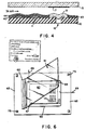
- the clam shell embodiment of Fig 6 provides a convenient fixture for the conservation of the protective gas layer (nitrogen or carbon dioxide) and if desired the alternation of such atmospheres with air, since one gas can be replaced by another in a rapid purging cycle.
- a phototool transparency 60 having opaque portions 61 is hinged at 62 to a mounting surface 63 to open and close a gas containing compartment having gas entry and exit ports 69.
- the photopolymer covered substrate 58 is registered by pegs 66, or the like.
- Closure or latching structure 68 is provided and rollers 75 for moving the fixture past a radiation source.
- the two photoexposure steps may also be reversed in order with particular advantage for some applications, as will become evident from the Fig 4 embodiment.
- the first exposure is made with an air blanket 39 in contact with the photopolymer layer surface, using a conventional off-contact phototool 15 with radiation blocking image patterns 17 thereon, and as before shown in the presence of un-collimated light.
- the photopolymer layer is polymerized below its surface 43 and has a liquid state surface covering 44, as conventionally expected with air inhibited liquid photopolymer surfaces. The curing is firmly bonded to the substrate surface.
- the second exposure step now follows through the transparency with a low energy flash after replacing the air blanket on the polymer surface with a non-reacting gas.
- the portion 19 remains in liquid polymer state throughout its layer thickness for washing out by solvent in a conventional development step.
- Photopolymer characteristics are critical to the performance of this method. For example, a high ratio of oxygen inhibition of the wet surface compared with that uncured polymer under the cured skin barrier surface is a novel requirement imposed by this invention.
- the production of chemical resistance of the polymerized portions to washout solvents with low radiant eneregy is also desirable as well as the bonding characteristics to the substrate surface.
- the photopolymer in the liquid state should be of a pastelike viscosity to be deposited as a layer on the substrate by screen printing or the like with no residual air bubbles on either surface. This screen printing could be prepatterned, if desired, in the manner described in my US-A-4,610,841.
- the photosensitivity to radiation should conform with the criteria hereinbefore described.
- EXAMPLE 1 SOLDER MASK PHOTOPOLYMER COMPOSITION WITH ENCHANCED PHOTOSENSITIVITY RATIO Parts by weight Ingredients 80 CELANESE CELRAD* 3600 UV/EP Resin 20 Trimethylopropane Triacrylate Diluent 1 CIBA-GEIGY IRGACURE* 500 Photoinitiator 1 MALLINKRODT Co. BYK-052 Defoamer 0.0003 Penn Color Co. PCN Green Pigment in Paste dispersion *Registered Trade Name
- This photopolymer has the following characteristics with a 5 kW (reducible to 2.5 kW) mercury metal halide lamp with peak output at 360 and 400 nanometer wavelengths:
- solder masks One important requirement for solder masks is the ability to plug or tent selected holes in the board, as shown at 12 in Fig 1. It is necessary to be able to plug the holes with hardened photopolymer to prevent molten solder from being pumped through the hole from the underside, thereby forcing solder up and under electrical components to cause short circuits.
- Holes of up to 0.08 cm in diameter were plugged by using the process of Examples 1 and 2, preceded by a coating step which forced liquid photopolymer into the holes, as depicted by photopolymer portion 14 bridging hole 12 (Fig 1).
- a squeegee was crafted so as to deposit extra liquid photopolymer into holes while maintaining the controlled thickness on the surface of the board.
- the leading edge of the squeege that is, the edge in contact with the screen fabric, was rounded, so as to deviate from the normal square edge.
- Holes so filled were subsequently permanently plugged by deleting the corresponding opaque areas 17 from phototransparency 15 so as to harden the photopolymer 14 in hole 12.
- the resulting skin layer photopatterns 13 may be displaced or shifted from the position of the corresponding phototransparency images. This shift is caused by the light rays 18 radiating from the source in a radial, not parallel pattern.
- the shadow cast on the photopolymer surface by the opaque areas 17, will therefore be in dimensional agreement with the phototransparency only for points directly beneath the lamp centerline.
- the deviation of the light rays might reach the order of fourteen degrees and the images formed in the photopolymer will be displaced by the order of 0.013 cm.
- This shift is corrected by using a photoreduced phototransparency image so that when the shift occurs the resulting photopatterns will be correctly registered with the features of substrate 10 and metal conductors 11 on the printed wiring board.
- a master phototransparency in dimensional agreement with the substrate is photoreduced by 0.07 percent in the Example 1 process to improve the registration.
- Salvaging reject printed wiring boards in the production process is readily done in this invention by controlling the amount of radiating energy before final bonding, as may be seen from the Fig 5 inspection station 59.
- the polymer Before a post inspection cure step more thoroughly bonding the polymer to the substrate is applied either in the process steps or as a separate bonding step at a later time, the polymer may be radiated just enough to bond the layer to the substrate so that it may be stripped without damage to an expensive circuit board thereunder.
- the liquid photopolymer of the former example was replaced by a dry film layer available form Dupont as "Product 730 S" consisting of a 0.008 cm thick photopolymer layer covered by a clear polyester sheet.
- This polymer was laminated onto the printed wiring substrate with the outer polyester sheet in place to protect the polymer from oxygen.
- a phototransparency with an opaque image thereon was placed in contact with the clear polyester sheet for a flash exposure for eight seconds from the 5 kW source at 1.5 m.
- the polyester sheet was peeled from the photopolymer surface to expose it to air, and the exposure followed with unpatterned radiation from the 2.5 kW source at 1.5 m for four minutes.
- the unstable state polymer was removed in a trichlorethane solvent to leave a fully stable state pattern.
- the final curing step prepared the product for acceptable solder mask properties in the presence of molten solder. This process was more critical than that with the liquid photopolymer of Example 1 because the differential photosensitivity in the presence of oxygen was not nearly as great as for the liquid photopolymer specially formulated for operation in this mode.
- Example 1 The process of Example 1 was repeated with a clear plastic film laminated over the liquid photopolymer as a means of excluding air from its surface rather than the non-reacting gas. After the first exposure the plastic film was peeled from the surface and the second exposure followed with comparable results.
Landscapes
- Engineering & Computer Science (AREA)
- Manufacturing & Machinery (AREA)
- Microelectronics & Electronic Packaging (AREA)
- Physics & Mathematics (AREA)
- General Physics & Mathematics (AREA)
- Exposure And Positioning Against Photoresist Photosensitive Materials (AREA)
- Manufacturing Of Printed Circuit Boards (AREA)
- Non-Metallic Protective Coatings For Printed Circuits (AREA)
Applications Claiming Priority (4)
| Application Number | Priority Date | Filing Date | Title |
|---|---|---|---|
| US110505 | 1980-01-08 | ||
| US11050587A | 1987-10-20 | 1987-10-20 | |
| US11085787A | 1987-10-21 | 1987-10-21 | |
| US110857 | 1998-07-07 |
Publications (2)
| Publication Number | Publication Date |
|---|---|
| EP0313111A2 true EP0313111A2 (de) | 1989-04-26 |
| EP0313111A3 EP0313111A3 (de) | 1991-05-02 |
Family
ID=26808085
Family Applications (1)
| Application Number | Title | Priority Date | Filing Date |
|---|---|---|---|
| EP19880200313 Withdrawn EP0313111A3 (de) | 1987-10-20 | 1988-02-22 | Photographische Belichtung mit Strahlungstransparenten Masken |
Country Status (3)
| Country | Link |
|---|---|
| EP (1) | EP0313111A3 (de) |
| JP (1) | JPH01116541A (de) |
| KR (1) | KR890007621A (de) |
Families Citing this family (1)
| Publication number | Priority date | Publication date | Assignee | Title |
|---|---|---|---|---|
| US4895760A (en) * | 1987-10-09 | 1990-01-23 | Tredegar Industries, Inc. | Film coating for rigid, smooth surfaces |
Family Cites Families (5)
| Publication number | Priority date | Publication date | Assignee | Title |
|---|---|---|---|---|
| US4429027A (en) * | 1981-05-21 | 1984-01-31 | E. I. Du Pont De Nemours & Co. | Photoimaging process |
| US4483884A (en) * | 1982-02-12 | 1984-11-20 | Union Carbide Corporation | Process for producing textured coatings |
| US4421784A (en) * | 1982-02-12 | 1983-12-20 | Union Carbide Corporation | Process for producing textured coatings |
| US4612270A (en) * | 1985-03-14 | 1986-09-16 | Rca Corporation | Two-layer negative resist |
| US4610941A (en) * | 1985-03-19 | 1986-09-09 | Sullivan Donald F | Method for photographically improving the resolution of screen printed photopolymer images |
-
1988
- 1988-02-22 EP EP19880200313 patent/EP0313111A3/de not_active Withdrawn
- 1988-02-24 KR KR1019880002007A patent/KR890007621A/ko not_active Withdrawn
- 1988-03-10 JP JP63057326A patent/JPH01116541A/ja active Pending
Also Published As
| Publication number | Publication date |
|---|---|
| KR890007621A (ko) | 1989-06-20 |
| JPH01116541A (ja) | 1989-05-09 |
| EP0313111A3 (de) | 1991-05-02 |
Similar Documents
| Publication | Publication Date | Title |
|---|---|---|
| US4971895A (en) | Double exposure method of photoprinting with liquid photopolymers | |
| US4506004A (en) | Printed wiring board | |
| US4260675A (en) | Photoprinting plate and method of preparing printed circuit board solder masks therewith | |
| US4424089A (en) | Photoprinting process and apparatus for exposing paste-consistency photopolymers | |
| US4966827A (en) | Polymer printing | |
| US5443672A (en) | Process for coating circuit boards | |
| US4752553A (en) | High resolution solder mask photopolymers for screen coating over circuit traces | |
| US4631111A (en) | Dichromic process for preparation of conductive circuit | |
| US4582778A (en) | Multi-function photopolymer for efficiently producing high resolution images on printed wiring boards, and the like | |
| JP3019503B2 (ja) | プリント配線板の製造方法 | |
| US4556627A (en) | Transferring polymer from thin plastic films to photodevelop insulation patterns on printed wiring boards | |
| EP0052806B1 (de) | Verfahren zum Vergrössern der Rasterpunkte in photopolymeren Lithomasken | |
| US4610941A (en) | Method for photographically improving the resolution of screen printed photopolymer images | |
| EP0130581B1 (de) | Vergrösserung von Photopolymerbildern in Photopolymervorlagen | |
| US4647524A (en) | Transferring polymer from thin plastic films to photodevelop insulation patterns on printed wiring boards | |
| EP0150623A2 (de) | Lichtempfindliches Schablonenmaterial | |
| US3751248A (en) | Method of selective multilayered etching | |
| USRE32430E (en) | Printed wiring board | |
| JP2743100B2 (ja) | プリント基板の製造方法、フォトソルダーレジストおよびソルダーレジストインキ | |
| US4539070A (en) | Exposure of photo resist | |
| US4560639A (en) | Reusable phototransparency image forming tools for direct contact printing | |
| US2007282A (en) | Method of producing a multicolor screen for the production of photographic color pictures | |
| JPH02144989A (ja) | プリント回路板の処理方法 | |
| JPH01116541A (ja) | 放射透過光工具によるフォトプリンティング | |
| JPH03256393A (ja) | プリント配線板の製造方法 |
Legal Events
| Date | Code | Title | Description |
|---|---|---|---|
| PUAI | Public reference made under article 153(3) epc to a published international application that has entered the european phase |
Free format text: ORIGINAL CODE: 0009012 |
|
| AK | Designated contracting states |
Kind code of ref document: A2 Designated state(s): DE FR GB IT NL |
|
| PUAL | Search report despatched |
Free format text: ORIGINAL CODE: 0009013 |
|
| AK | Designated contracting states |
Kind code of ref document: A3 Designated state(s): DE FR GB IT NL |
|
| STAA | Information on the status of an ep patent application or granted ep patent |
Free format text: STATUS: THE APPLICATION IS DEEMED TO BE WITHDRAWN |
|
| 18D | Application deemed to be withdrawn |
Effective date: 19910301 |