EP0313683A1 - Méthode pour fabriquer une structure de circuit intégré semi-conducteur comprenant un élément de longueur submicrométrique - Google Patents
Méthode pour fabriquer une structure de circuit intégré semi-conducteur comprenant un élément de longueur submicrométrique Download PDFInfo
- Publication number
- EP0313683A1 EP0313683A1 EP87115967A EP87115967A EP0313683A1 EP 0313683 A1 EP0313683 A1 EP 0313683A1 EP 87115967 A EP87115967 A EP 87115967A EP 87115967 A EP87115967 A EP 87115967A EP 0313683 A1 EP0313683 A1 EP 0313683A1
- Authority
- EP
- European Patent Office
- Prior art keywords
- layer
- polycrystalline silicon
- silicon
- portions
- silicon dioxide
- Prior art date
- Legal status (The legal status is an assumption and is not a legal conclusion. Google has not performed a legal analysis and makes no representation as to the accuracy of the status listed.)
- Ceased
Links
Images


Classifications
-
- H—ELECTRICITY
- H10—SEMICONDUCTOR DEVICES; ELECTRIC SOLID-STATE DEVICES NOT OTHERWISE PROVIDED FOR
- H10D—INORGANIC ELECTRIC SEMICONDUCTOR DEVICES
- H10D30/00—Field-effect transistors [FET]
- H10D30/01—Manufacture or treatment
- H10D30/021—Manufacture or treatment of FETs having insulated gates [IGFET]
- H10D30/0223—Manufacture or treatment of FETs having insulated gates [IGFET] having source and drain regions or source and drain extensions self-aligned to sides of the gate
-
- H—ELECTRICITY
- H10—SEMICONDUCTOR DEVICES; ELECTRIC SOLID-STATE DEVICES NOT OTHERWISE PROVIDED FOR
- H10P—GENERIC PROCESSES OR APPARATUS FOR THE MANUFACTURE OR TREATMENT OF DEVICES COVERED BY CLASS H10
- H10P14/00—Formation of materials, e.g. in the shape of layers or pillars
- H10P14/60—Formation of materials, e.g. in the shape of layers or pillars of insulating materials
- H10P14/63—Formation of materials, e.g. in the shape of layers or pillars of insulating materials characterised by the formation processes
- H10P14/6302—Non-deposition formation processes
- H10P14/6304—Formation by oxidation, e.g. oxidation of the substrate
- H10P14/6306—Formation by oxidation, e.g. oxidation of the substrate of the semiconductor materials
- H10P14/6308—Formation by oxidation, e.g. oxidation of the substrate of the semiconductor materials of Group IV semiconductors
-
- H—ELECTRICITY
- H10—SEMICONDUCTOR DEVICES; ELECTRIC SOLID-STATE DEVICES NOT OTHERWISE PROVIDED FOR
- H10P—GENERIC PROCESSES OR APPARATUS FOR THE MANUFACTURE OR TREATMENT OF DEVICES COVERED BY CLASS H10
- H10P50/00—Etching of wafers, substrates or parts of devices
- H10P50/20—Dry etching; Plasma etching; Reactive-ion etching
- H10P50/26—Dry etching; Plasma etching; Reactive-ion etching of conductive or resistive materials
- H10P50/264—Dry etching; Plasma etching; Reactive-ion etching of conductive or resistive materials by chemical means
- H10P50/266—Dry etching; Plasma etching; Reactive-ion etching of conductive or resistive materials by chemical means by vapour etching only
- H10P50/267—Dry etching; Plasma etching; Reactive-ion etching of conductive or resistive materials by chemical means by vapour etching only using plasmas
- H10P50/268—Dry etching; Plasma etching; Reactive-ion etching of conductive or resistive materials by chemical means by vapour etching only using plasmas of silicon-containing layers
-
- H—ELECTRICITY
- H10—SEMICONDUCTOR DEVICES; ELECTRIC SOLID-STATE DEVICES NOT OTHERWISE PROVIDED FOR
- H10P—GENERIC PROCESSES OR APPARATUS FOR THE MANUFACTURE OR TREATMENT OF DEVICES COVERED BY CLASS H10
- H10P50/00—Etching of wafers, substrates or parts of devices
- H10P50/73—Etching of wafers, substrates or parts of devices using masks for insulating materials
-
- H—ELECTRICITY
- H10—SEMICONDUCTOR DEVICES; ELECTRIC SOLID-STATE DEVICES NOT OTHERWISE PROVIDED FOR
- H10P—GENERIC PROCESSES OR APPARATUS FOR THE MANUFACTURE OR TREATMENT OF DEVICES COVERED BY CLASS H10
- H10P76/00—Manufacture or treatment of masks on semiconductor bodies, e.g. by lithography or photolithography
- H10P76/40—Manufacture or treatment of masks on semiconductor bodies, e.g. by lithography or photolithography of masks comprising inorganic materials
- H10P76/408—Manufacture or treatment of masks on semiconductor bodies, e.g. by lithography or photolithography of masks comprising inorganic materials characterised by their sizes, orientations, dispositions, behaviours or shapes
- H10P76/4085—Manufacture or treatment of masks on semiconductor bodies, e.g. by lithography or photolithography of masks comprising inorganic materials characterised by their sizes, orientations, dispositions, behaviours or shapes characterised by the processes involved to create the masks
-
- Y—GENERAL TAGGING OF NEW TECHNOLOGICAL DEVELOPMENTS; GENERAL TAGGING OF CROSS-SECTIONAL TECHNOLOGIES SPANNING OVER SEVERAL SECTIONS OF THE IPC; TECHNICAL SUBJECTS COVERED BY FORMER USPC CROSS-REFERENCE ART COLLECTIONS [XRACs] AND DIGESTS
- Y10—TECHNICAL SUBJECTS COVERED BY FORMER USPC
- Y10S—TECHNICAL SUBJECTS COVERED BY FORMER USPC CROSS-REFERENCE ART COLLECTIONS [XRACs] AND DIGESTS
- Y10S257/00—Active solid-state devices, e.g. transistors, solid-state diodes
- Y10S257/90—MOSFET type gate sidewall insulating spacer
-
- Y—GENERAL TAGGING OF NEW TECHNOLOGICAL DEVELOPMENTS; GENERAL TAGGING OF CROSS-SECTIONAL TECHNOLOGIES SPANNING OVER SEVERAL SECTIONS OF THE IPC; TECHNICAL SUBJECTS COVERED BY FORMER USPC CROSS-REFERENCE ART COLLECTIONS [XRACs] AND DIGESTS
- Y10—TECHNICAL SUBJECTS COVERED BY FORMER USPC
- Y10S—TECHNICAL SUBJECTS COVERED BY FORMER USPC CROSS-REFERENCE ART COLLECTIONS [XRACs] AND DIGESTS
- Y10S438/00—Semiconductor device manufacturing: process
- Y10S438/942—Masking
- Y10S438/947—Subphotolithographic processing
-
- Y—GENERAL TAGGING OF NEW TECHNOLOGICAL DEVELOPMENTS; GENERAL TAGGING OF CROSS-SECTIONAL TECHNOLOGIES SPANNING OVER SEVERAL SECTIONS OF THE IPC; TECHNICAL SUBJECTS COVERED BY FORMER USPC CROSS-REFERENCE ART COLLECTIONS [XRACs] AND DIGESTS
- Y10—TECHNICAL SUBJECTS COVERED BY FORMER USPC
- Y10S—TECHNICAL SUBJECTS COVERED BY FORMER USPC CROSS-REFERENCE ART COLLECTIONS [XRACs] AND DIGESTS
- Y10S438/00—Semiconductor device manufacturing: process
- Y10S438/942—Masking
- Y10S438/948—Radiation resist
- Y10S438/95—Multilayer mask including nonradiation sensitive layer
Definitions
- This invention relates to a method for fabricating semiconductor integrated circuit structures which have field effect transistor devices therein having a submicrometer gate length.
- This layer is then subjected to an anisotropic etching process such as by reactive ion etching, to substantially remove the horizontal layer while leaving the vertical layer substantially intact.
- the vertical layer dimension is adjusted depending on the original thickness of the layer applied. In this way a narrow dimension region such as a field effect transistor gate of submicrometer length can be obtained.
- Another approach uses a tri-layer resist system to define the gate electrode of a field effect transistor by photo- or E-beam lithography.
- a comparatively thick bottom polymer- or resist layer is deposited on the surface of a polycrystalline silicon layer which is designated to be in part the gate electrode.
- an intermediate barrier layer of silicon dioxide or nitride is deposited by chemical vapor deposition at room temperature.
- the top layer is a highly sensitive positive photoresist layer in which the desired pattern of the gate electrode is generated by optical or E-beam exposure and development. Pattern transfer from the top resist to the silicon dioxide or nitride barrier layer is achieved by plasma etching with CF4.
- An oxygen RIE process is used to transfer the pattern to the bottom polymer- or resist layer.
- the bottom resist layer is oxygen etched at a relatively high pressure for obtaining lateral bias etching of the silicon dioxide/nitride barrier layer by a particular amount.
- the resulting bottom layer photoresist bars decreased by the line width bias over the original line width of the top resist layer, serve as a photoresist mask for the subsequent polycrystalline silicon RIE step.
- This step has poor dimensional control as it is known that the base of the photoresist bars is not exactly defined and differs in width to a considerable extent from the wafer center to the edge.
- the lateral oxygen etch rate is not constant with respect to time, and the average line width bias is limited by the geometry.
- a method for fabricating a semiconductor integrated circuit structure having a submicrometer length device element wherein a surface isolation pattern is formed in a semiconductor substrate which isolates regions of the semiconductor within the substrate from one another. These semiconductor regions are designated to contain devices.
- a first insulating compound layer is formed on the surface of the semiconductor substrate which is designated to be in part the gate dielectric layer.
- a polycrystalline silicon layer is deposited on this insulating compound layer. The polycrystalline silicon layer is heavily doped by ion implantation and annealed below about 850°C. The polycrystalline silicon layer is dry-etched to leave polycrystalline silicon portions with sidewall angles of at least 90°.
- the polycrystalline silicon portions are thermally oxidized, and the thermal oxide is removed to leave polycrystalline silicon portions of reduced submicrometer thickness and length. Subsequently, the desired pattern of PN junctions is formed in the semiconductor substrate, using, for example, ion implantation techniques, with the controlled submicrometer length polycrystalline silicon portions serving as a mask.
- a second insulating layer is deposited on the polycrystalline silicon layer.
- the second insulating layer as well as the polycrystalline silicon layer are patterned by dry etching. The caps remaining of the second insulating layer on the polycrystalline silicon portions prevent a surface oxidation but allow a lateral oxidation of these portions.
- the method described in the preceding paragraph may find particular application for the formation of submicrometer gate length field effect transistor devices in an integrated circuit structure.
- the first insulating compound layer is formed of a combination of silicon dioxide of about 4 to 6 nm, of silicon nitride of about 11 to 15 nm, and of silicon dioxide of about 1.0 to 1.5 nm thickness.
- the polycrystalline silicon layer has a thickness in the range of about 350 to 650 nm.
- the doping of this layer is preferably done by ion implantation of phosphorus or arsenic at a dose in the range of about 1 to 4 x 10¹⁶/cm2 at approximately 40 to 80 KeV.
- the polycrystalline silicon layer is annealed at about 800°C to produce a higher phosphorus or arsenic ion concentration in its upper part.
- the pattern of polycrystalline silicon portions with substantially vertical sidewalls is preferably made by RIE etching using an etching gas composition of about 6 to 8 % b.v. SF6, 2 to 3 % b.v. Cl2, remainder He, and a comparatively low power density of about 0.1 to 0.3 W/cm2.
- the high concentration of doping material in the polycrystalline silicon layer allows thermal oxidation of this layer at a lower temperature than previously used, namely at a temperature of about 800°C. This concentration also allows a uniform thermal growth of silicon dioxide which is easily to be controlled.
- the method of the invention mitigates these shortcomings of the prior art by using a polycrystalline silicon layer which is implanted at a high ion dose and annealed at about 800 to 850°C which later on provides for an extremely uniform thermal oxide growth on the underlying polycrystalline silicon in a shorter period than previously.
- the thickness of the oxidation blocking material on the polycrystalline silicon layer is now in the order of several nm only so that a dry etching step of very short duration is sufficient for its removal.
- Figs. 1A, B through 7 there are illustrated two embodiments for fabricating submicrometer channel length field effect transistors in a high density integrated circuit structure.
- the process is illustrated to form N channel MOSFET integrated circuits.
- P channel field effect transistors can alternatively be formed by the present embodiments by simply reversing the polarity of the various elements of the transistors and associated regions.
- the first series of steps involve the formation of the isolation regions for isolating regions of monocrystalline silicon from other regions of monocrystalline silicon in a P- ⁇ 100> crystallographic oriented silicon substrate (10) as thus can be seen with reference to Figs. 1A and B.
- the isolation may preferably be partial dielectric isolation using materials such as silicon dioxide, glass, polyimide, etc., alone or in combinations.
- the preferred pattern of partial dielectric isolation (12) defines monocrystalline silicon surface regions wherein field effect devices will ultimately be formed.
- dielectric isolation regions of this type For example, detailed processes for forming dielectric isolation regions are described in U. S. Patents Nos. 4,104,086 and 4,471,523.
- a P+ region (14) is typically formed under the dielectric isolation layer region (12) to prevent a formation of an inversion layer and the resulting electrical leakage between isolated monocrystalline regions under the isolation region (12).
- the recessed dielectric isolation region (12) and P+ region (14) may be formed by first thermally oxidising the surface of the silicon substrate (10) to form a silicon dioxide layer (not shown) thereon. A silicon nitride layer (not shown) is then deposited by chemical vapor deposition thereover. The silicon nitride layer has openings formed therein at the desired location of the isolation regions by conventional lithography and etching techniques.
- the P+ region (14) is formed by the ion implantation of boron through the silicon dioxide layer in the openings in the silicon nitride layer. The silicon nitride layer forms an effective mask to the penetration of the boron ions in the remaining areas covering the surface of the wafer.
- the recessed oxide isolation region (12) is then grown by placing the wafer in an oxidation ambient for a time sufficient to form the recessed oxidation regions (12).
- the silicon nitride and silicon dioxide layers are now removed from the surface of the silicon wafer.
- the surface isolation pattern in the semiconductor silicon substrate which isolates regions of the semiconductor within the substrate from one another is now formed.
- An insulating layer (16) is formed on the surface of the silicon body (10).
- This layer may be thermally grown silicon dioxide which is designated to be in part the gate dielectric layer upon the surface of the silicon substrate.
- this layer may be composed of silicon dioxide, silicon nitride, nitrided silicon dioxide, silicon dioxide implanted with N2 ions, polycrystalline aluminum trioxide or the like or combinations of the foregoing. The layer thickness of these materials is not noticeably changed by subsequent thermal oxidation.
- the insulating layer is formed of a combination of silicon dioxide (16.1), silicon nitride (16.2), and silicon dioxide (16.3).
- the thicknesses of the individual layers are, for example, of 4 to 6 nanometers silicon dioxide (16.1), of 11 to 15 nanometers silicon nitride (16.2), and of 1.0 to 1.5 nanometers silicon dioxide (16.3).
- Silicon nitride and silicon dioxide layers 16.2 and 16.3 cover the entire surface having the surface isolation pattern (12) and over the silicon dioxide layer (16.1).
- the silicon dioxide layers are preferably thermally grown in oxygen or oxygen-water vapor ambient at a temperature of about 800°C.
- a second method for growing silicon dioxide involves a chemical vapor deposition process wherein SiO2 is deposited by using SiH4 and O2 at about 450°C under atmospheric or low pressure conditions.
- the silicon nitride layer is usually formed by chemical vapor deposition using the following process conditions: SiH4, NH3 and N2 carrier gas at a temperature of about 800°C under atmospheric or low pressure conditions.
- the surface conductivity of the P- substrate (10) is adjusted where the field effect transistors are to be formed.
- the threshold, Vt is adjusted by using for example a boron ion implantation of about 1.2 x 10¹²/cm2 dose at approximately 7 KeV to produce surface P regions (18).
- polycrystalline silicon layer (20) onto the entire surface of silicon dioxide/silicon nitride/silicon dioxide compound layer (16.1.2.3).
- the polycrystalline silicon layer is deposited by using silane in a hydrogen ambient in the temperature range of about 600°C to 650°C, and preferably about 625°C.
- the operative thickness of the polycrystalline silicon layer is between about 350 to 650 nanometers with 430 nanometers being preferred.
- the polycrystalline silicon layer makes no electrical contact to the silicon body (10) since it is formed upon insulating compound layer (16).
- the entire surface of polycrystalline silicon layer (20) is then doped by ion implantation of phosphorus or arsenic and heating process.
- the polycrystalline silicon layer (20) is implanted at a phosphorus ion dose in the range of about 1 to 4 x 10¹⁶/cm2 at approximately 40 to 80 KeV.
- the wafers are annealed in N2 for about one hour in the temperature range of about 800 to 850°C.
- This annealing treatment causes a distribution of the phosphorus ions in the polycrystalline silicon layer resulting in a higher phosphorus concentration in the upper part of the layer.
- phosphorus concentration profiles measured in an about 430 nm thick polycrystalline silicon layer show in the top quarter a phosphorus ion concentration about twice as high as in the remainder of the layer.
- This concentration profile which depends on the implantation energy and on the annealing temperatures is important for later oxidation and etching processes. If annealing would take place at higher temperatures, for example at about 900 to 1.000°C, a complete redistribution of the implanted phosphorus ions would take place resulting in a constant concentration throughout polycrystalline silicon layer (20).
- a double layer of silicon dioxide/silicon nitride is formed on polycristalline silicon layer (20), which is used later on to define portions of polycrystalline silicon and which prevents surface oxidation but allows lateral oxidation of these portions.
- Silicon dioxide layer (22.1, Fig. 1B) is thermally grown or deposited by chemical vapor deposition on polycrystalline silicon layer (20), and silicon nitride layer (22.2) is deposited by chemical vapor deposition on silicon dioxide layer (22.1) using the process conditions as mentioned before.
- the thicknesses of these layers are, for example, of 5 to 8 nanometers silicon dioxide and of 4 to 6 nanometers silicon nitride.
- an insulating layer (22) can be formed on polycrystalline silicon layer (20) in the same step as the doping of this layer is effected by implanting ions which contain nitrogen in addition to phosphorus.
- ions which contain nitrogen in addition to phosphorus.
- species like PN2+ are implanted with a dose of the order of 2.1 x 10¹⁶/cm2 and 50 KeV followed by an annealing step of 1 hr at about 850°C in N2+.
- the phosphorus ions distribute throughout polycrystalline silicon layer (20) whereas the nitrogen ions migrate to the surface of this layer to form surface nitride layer (22) thereon. Details on the mechanism of molecular nitrogen ion (N2+) implantation can be found for example in W. J. M. J. Josquin et al, J. Electrochem. Soc., Vol. 129, No. 8, August 1982, pp. 1803.
- photoresist mask (24, Figs. 2A, B) on polycrystalline silicon layer (20)
- a standard photo-lithographic process is used. In this process a photoresist is applied in a thickness of about 1 ⁇ m to the surface of polycrystalline silicon layer (20).
- a variety of known positive resists are suitable for this purpose, for example the AZ 1450J photoresist of the Shipley Comp.
- Patterning of an AZ photoresist layer is carried out by means of a known UV exposure tool using a 436 nm wavelength exposure followed by a baking step in the temperature range of about 95 to 105 oC for about 30 minutes in N2 and development in an aqueous AZ developer based upon tetramethylammonium hydroxide.
- a tri-layer resist system can be used for making the photoresist mask.
- an about 1 to 3 ⁇ m thick polymer- or resist layer (24.1) is deposited on the surface of polycrystalline silicon layer (20) followed by a baking step at about 210°C for about 30 minutes.
- An intermediate masking layer (24.2) of silicon nitride is then deposited in a thickness of 0.1 to 0.2 ⁇ m by plasma-enhanced CVD at room temperature.
- the top layer (24.3) is a 0.2 to 1 ⁇ m thick layer of a highly sensitive positive photoresist in which the desired pattern is generated as described above. For patterns with submicrometer dimensions E-beam exposure is used.
- Pattern transfer from the top resist to the silicon nitride (24.2) is achieved by plasma etching with CF4 at about 66.5 ⁇ bar.
- An oxygen reactive ion etch process is used to transfer the pattern to the bottom polymer- or resist layer.
- a 0.1 W/cm2 RF power density at a pressure of about 5 ⁇ bar resulted in a 70 nm/min etch rate.
- this tri-layer process step yields strictly vertical photoresist sidewalls.
- etching step is anisotropic such as reactive ion etching, RIE, in SF6/Cl2/He.
- RIE reactive ion etching
- a CF4 etching step may precede to remove the native oxide from the polycrystalline silicon.
- the process for reducing the FET channel length by removing controllable quantities of the polycrystalline silicon portions covering these device regions can only be successfully conducted if, by anisotropic etching, polycrystalline silicon portions with sidewall angles of 90 degrees, preferably of 90 to 92 degrees are obtainable.
- polycrystalline silicon portions with sidewall angles of 90 degrees preferably of 90 to 92 degrees are obtainable.
- trenches are formed in the silicon dioxide/silicon nitride compound gate (16.2, 16.3) at the lower end of the polycrystalline silicon sidewall which make the devices unserviceable. Therefore, an etching process had to be developed which provides for good selectivity between polycrystalline silicon and silicon nitride and silicon dioxide respectively, and which generates 90 degree angles.
- RIE trenching at the lower end of the polycrystalline silicon sidewalls RIE has to be carried out at low power density, preferably at about 0.1 to 0.3 W/cm2 up to the endpoint and, from there, at ⁇ 0.05 W/cm2 with about 15 % overetching.
- the etching endpoint is determinded by means of laser interference.
- polycrystalline silicon layer (20) is etched in the areas exposed by photoresist mask (24) or (24.1, Figs. 2A, B) with the following parameters:
- the remaining photoresist etching mask is removed by isotropic stripping in an oxygen plasma to leave the Fig. 3A structure with vertical polycrystalline silicon sidewalls.
- the etching of double layer of silicon dioxide/silicon nitride (22.1, 22.2, Fig. 1B) arranged on polycrystalline silicon layer (20) has to be carried out using an etching gas different from that for the etching of polycrystalline silicon.
- This etching step is also a reactive ion etch, RIE, in a CF4 plasma.
- RIE reactive ion etch
- the double layer is etched in the areas exposed by photoresist mask (24) of Fig. 2B, which is generated as described before, with the following parameters:
- This etching step also removes native oxide from the polycrystalline silicon surface.
- polycrystalline silicon layer (20) is etched in the same chamber, using SF6/Cl2/He as etching gas and the parameters described above.
- the photoresist mask is removed in an oxygen plasma to leave the Fig. 3B structure with vertical polycrystalline silicon sidewalls.
- the oxidation of undoped or in situ doped polycrystalline silicon with a homogenous distribution of doping material is difficult to control, because the oxidation rates at the upper and at the lower end of the sidewalls of the respective polycrystalline silicon portions differ, and projections (horns) are formed at the upper end.
- a higher concentration of phosphorus or arsenic ions is chosen for the upper part of polycrystalline silicon layer (20), which increases the oxidation rate of this part.
- the thermal oxide (26) is removed from all surfaces of polycrystalline silicon portions (20) such as by plasma etching or wet etching in concentrated hydrofluoric acid with silicon nitride layer (16.2) acting as an etch barrier.
- polycrystalline silicon portions (20, Fig. 5A) are obtained with length and thickness dimensions reduced by the desired amount.
- silicon dioxide is thermally grown at about 800°C in a thickness of about 333 nm on a portion of polycrystalline silicon layer (20) having a length of 0.9 ⁇ m and a thickness of 0.45 ⁇ m. After removal of the oxide with concentrated hydrofluoric acid a structure having a length of 0.60 ⁇ m and a thickness of 0.30 ⁇ m is obtained. The oxide was grown in the required thickness within about four hours. The reduction in thickness of the polycrystalline silicon portion is compensated for by the deposition of a correspondingly thicker polycrystalline silicon layer (20).
- a cap (22.1, 22.2 Fig. 3B).
- this cap may consist of silicon nitride in a layer thickness of about 100 nm.
- the maximum nitride layer thickness of the present invention should not exceed 4 to 6 nanometers. It turned out that, owing to this small thickness, the silicon nitride layer was destroyed by stresses generated during the lateral oxidation of the polycrystalline silicon portions, and failed to prevent the oxidation of the horizontal surfaces of these portions.
- a stress-relieve layer consisting of silicon dioxide and having a thickness about 5 to 8 nanometers, which effectively prevents the destruction of the silicon nitride layer during oxidation, is arranged between the polycrystalline silicon layer and the silicon nitride layer.
- the process steps for the deposition of silicon dioxide and silicon nitride layers (22.1 and 22.2) have been described above with reference to Fig. 1B.
- Fig. 4B when the structure is subjected to conventional thermal oxidation, controllable quantities of the polycrystalline silicon portion (20) are consumed laterally beneath the silicon dioxide/silicon nitride cap (22.1, 22.2) to produce silicon dioxide portions (26).
- polycrystalline silicon portion (20) With the consumption of polycrystalline silicon in the formation of silicon dioxide portions (26), the lengths of polycrystalline silicon portion (20) may be reduced from about 0.72 ⁇ m or 0.75 ⁇ m down to about 0.29 ⁇ m and 0.33 ⁇ m respectively. Finally, silicon dioxide portions (26) and silicon dioxide/silicon nitride cap (22.1, 22.2) are simultaneously removed by etching techniques to leave the polycrystalline silicon portion (20, Fig. 5B) having the required narrowed lateral dimensions.
- polycrystalline silicon portion (20) being the gate electrode of the field effect transistor device.
- the exposed compound gate dielectric silicon dioxide/silicon nitride/ silicon dioxide (16.1,2,3) can either be removed by etching followed by the implantation or diffusion of phosphorus or arsenic dopants adjacent to the gate electrode to form the desired PN junction source/drain elements for the field effect transistor device, or the compound gate dielectric can be allowed to remain and ion implantation with the appropriate energy to penetrate this compound layer is used to form the N+ source/drain regions in the device areas.
- One example of the ion implantation method uses arsenic as the conductivity imparting impurity of the order of 2.0 x 10¹⁵ ions/cm2 and 80 KeV to form a PN junction of 0.4 ⁇ m depth.
- a conformal chemically vapor deposited silicon dioxide or the like insulator layer (not shown) is formed over the entire device structure.
- One preferred method European Patent Application 86104596.1
- for making such an insulator layer by chemical vapor deposition under reduced pressure uses tetraethylorthosilicate (TEOS) as a source for silicon and oxygen, which is directed across the heated substrates.
- TEOS tetraethylorthosilicate
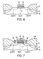
- Anisotropic etching is utilized to remove the horizontal conformal chemical vapor deposition layer and leave the spacer sidewall silicon dioxide layers (28) on the sides of polycrystalline silicon portion (20).
- the spacers (28) are shown in Fig. 6.
- Fig. 7 also illustrates the result of the formation of the phosphosilicate glass insulating layer (34) and the metal electrical contacts (36) to the various elements of the devices. It is also feasable to form a polycide layer (not shown) on top of the polycrystalline silicon layer (20) to lower its sheet resistance. Details relating to anisotropic etching of polycide layers are described, for instance, by L. Epraph in the IEEE Transactions on Electron Devices, Vol. ED-28, No. 11, November 1981, pp. 1315-1319.
Landscapes
- Insulated Gate Type Field-Effect Transistor (AREA)
- Formation Of Insulating Films (AREA)
- Element Separation (AREA)
Priority Applications (3)
| Application Number | Priority Date | Filing Date | Title |
|---|---|---|---|
| EP87115967A EP0313683A1 (fr) | 1987-10-30 | 1987-10-30 | Méthode pour fabriquer une structure de circuit intégré semi-conducteur comprenant un élément de longueur submicrométrique |
| JP63233857A JPH0654781B2 (ja) | 1987-10-30 | 1988-09-20 | 集積回路構造体の製造方法 |
| US07/259,082 US4869781A (en) | 1987-10-30 | 1988-10-17 | Method for fabricating a semiconductor integrated circuit structure having a submicrometer length device element |
Applications Claiming Priority (1)
| Application Number | Priority Date | Filing Date | Title |
|---|---|---|---|
| EP87115967A EP0313683A1 (fr) | 1987-10-30 | 1987-10-30 | Méthode pour fabriquer une structure de circuit intégré semi-conducteur comprenant un élément de longueur submicrométrique |
Publications (1)
| Publication Number | Publication Date |
|---|---|
| EP0313683A1 true EP0313683A1 (fr) | 1989-05-03 |
Family
ID=8197405
Family Applications (1)
| Application Number | Title | Priority Date | Filing Date |
|---|---|---|---|
| EP87115967A Ceased EP0313683A1 (fr) | 1987-10-30 | 1987-10-30 | Méthode pour fabriquer une structure de circuit intégré semi-conducteur comprenant un élément de longueur submicrométrique |
Country Status (3)
| Country | Link |
|---|---|
| US (1) | US4869781A (fr) |
| EP (1) | EP0313683A1 (fr) |
| JP (1) | JPH0654781B2 (fr) |
Cited By (3)
| Publication number | Priority date | Publication date | Assignee | Title |
|---|---|---|---|---|
| DE3915650A1 (de) * | 1989-05-12 | 1990-11-15 | Siemens Ag | Verfahren zur strukturierung einer auf einem halbleiterschichtaufbau angeordneten schicht |
| WO2005071724A1 (fr) * | 2004-01-14 | 2005-08-04 | Tokyo Electron Limited | Procede d'ajustage d'une structure d'electrode de grille |
| WO2005104218A1 (fr) * | 2004-03-31 | 2005-11-03 | Tokyo Electron Limited | Procede pour commander le decoupage d'une structure d'electrode de grille |
Families Citing this family (56)
| Publication number | Priority date | Publication date | Assignee | Title |
|---|---|---|---|---|
| US5089863A (en) * | 1988-09-08 | 1992-02-18 | Mitsubishi Denki Kabushiki Kaisha | Field effect transistor with T-shaped gate electrode |
| US5543646A (en) * | 1988-09-08 | 1996-08-06 | Mitsubishi Denki Kabushiki Kaisha | Field effect transistor with a shaped gate electrode |
| US5271799A (en) * | 1989-07-20 | 1993-12-21 | Micron Technology, Inc. | Anisotropic etch method |
| US5201993A (en) * | 1989-07-20 | 1993-04-13 | Micron Technology, Inc. | Anisotropic etch method |
| US4971655A (en) * | 1989-12-26 | 1990-11-20 | Micron Technology, Inc. | Protection of a refractory metal silicide during high-temperature processing using a dual-layer cap of silicon dioxide and silicon nitride |
| JPH07108988B2 (ja) * | 1990-04-11 | 1995-11-22 | 株式会社島津製作所 | マイクロメカニクスの製造方法 |
| US5013398A (en) * | 1990-05-29 | 1991-05-07 | Micron Technology, Inc. | Anisotropic etch method for a sandwich structure |
| US5094712A (en) * | 1990-10-09 | 1992-03-10 | Micron Technology, Inc. | One chamber in-situ etch process for oxide and conductive material |
| US5436481A (en) * | 1993-01-21 | 1995-07-25 | Nippon Steel Corporation | MOS-type semiconductor device and method of making the same |
| SE501079C2 (sv) * | 1993-04-16 | 1994-11-07 | Asea Brown Boveri | Metod för etsning av kiselområden på isolerande substrat |
| US6780718B2 (en) | 1993-11-30 | 2004-08-24 | Stmicroelectronics, Inc. | Transistor structure and method for making same |
| JP3336747B2 (ja) * | 1994-06-09 | 2002-10-21 | ソニー株式会社 | 絶縁膜の形成方法、並びに半導体装置の作製方法及び半導体装置 |
| US5917219A (en) * | 1995-10-09 | 1999-06-29 | Texas Instruments Incorporated | Semiconductor devices with pocket implant and counter doping |
| US6049135A (en) | 1996-05-28 | 2000-04-11 | Kabushiki Kaisha Toshiba | Bed structure underlying electrode pad of semiconductor device and method for manufacturing same |
| US6037627A (en) * | 1996-08-02 | 2000-03-14 | Seiko Instruments Inc. | MOS semiconductor device |
| US5796151A (en) * | 1996-12-19 | 1998-08-18 | Texas Instruments Incorporated | Semiconductor stack having a dielectric sidewall for prevention of oxidation of tungsten in tungsten capped poly-silicon gate electrodes |
| JP3090074B2 (ja) * | 1997-01-20 | 2000-09-18 | 日本電気株式会社 | 半導体装置及びその製造方法 |
| US5763922A (en) * | 1997-02-28 | 1998-06-09 | Intel Corporation | CMOS integrated circuit having PMOS and NMOS devices with different gate dielectric layers |
| US6048769A (en) | 1997-02-28 | 2000-04-11 | Intel Corporation | CMOS integrated circuit having PMOS and NMOS devices with different gate dielectric layers |
| US6080629A (en) * | 1997-04-21 | 2000-06-27 | Advanced Micro Devices, Inc. | Ion implantation into a gate electrode layer using an implant profile displacement layer |
| US5885877A (en) * | 1997-04-21 | 1999-03-23 | Advanced Micro Devices, Inc. | Composite gate electrode incorporating dopant diffusion-retarding barrier layer adjacent to underlying gate dielectric |
| US5963841A (en) * | 1997-08-01 | 1999-10-05 | Advanced Micro Devices, Inc. | Gate pattern formation using a bottom anti-reflective coating |
| US5776821A (en) * | 1997-08-22 | 1998-07-07 | Vlsi Technology, Inc. | Method for forming a reduced width gate electrode |
| US6204130B1 (en) * | 1997-08-29 | 2001-03-20 | Advanced Micro Devices, Inc. | Semiconductor device having reduced polysilicon gate electrode width and method of manufacture thereof |
| US6087238A (en) * | 1997-12-17 | 2000-07-11 | Advanced Micro Devices, Inc. | Semiconductor device having reduced-width polysilicon gate and non-oxidizing barrier layer and method of manufacture thereof |
| US6033998A (en) * | 1998-03-09 | 2000-03-07 | Lsi Logic Corporation | Method of forming variable thickness gate dielectrics |
| US6509606B1 (en) | 1998-04-01 | 2003-01-21 | National Semiconductor Corporation | Single poly EPROM cell having smaller size and improved data retention compatible with advanced CMOS process |
| US5880006A (en) * | 1998-05-22 | 1999-03-09 | Vlsi Technology, Inc. | Method for fabrication of a semiconductor device |
| US6054206A (en) * | 1998-06-22 | 2000-04-25 | Novellus Systems, Inc. | Chemical vapor deposition of low density silicon dioxide films |
| US6110779A (en) | 1998-07-17 | 2000-08-29 | Advanced Micro Devices, Inc. | Method and structure of etching a memory cell polysilicon gate layer using resist mask and etched silicon oxynitride |
| US6380055B2 (en) | 1998-10-22 | 2002-04-30 | Advanced Micro Devices, Inc. | Dopant diffusion-retarding barrier region formed within polysilicon gate layer |
| US6746925B1 (en) * | 2003-03-25 | 2004-06-08 | Lsi Logic Corporation | High-k dielectric bird's beak optimizations using in-situ O2 plasma oxidation |
| US6790720B1 (en) * | 2003-09-25 | 2004-09-14 | Macronix International Co., Ltd. | Method for fabricating a MOSFET and reducing line width of gate structure |
| JP2008124399A (ja) * | 2006-11-15 | 2008-05-29 | Toshiba Corp | 半導体装置の製造方法 |
| US9461169B2 (en) | 2010-05-28 | 2016-10-04 | Globalfoundries Inc. | Device and method for fabricating thin semiconductor channel and buried strain memorization layer |
| US8592328B2 (en) | 2012-01-20 | 2013-11-26 | Novellus Systems, Inc. | Method for depositing a chlorine-free conformal sin film |
| US9214333B1 (en) * | 2014-09-24 | 2015-12-15 | Lam Research Corporation | Methods and apparatuses for uniform reduction of the in-feature wet etch rate of a silicon nitride film formed by ALD |
| US9589790B2 (en) | 2014-11-24 | 2017-03-07 | Lam Research Corporation | Method of depositing ammonia free and chlorine free conformal silicon nitride film |
| US9564312B2 (en) | 2014-11-24 | 2017-02-07 | Lam Research Corporation | Selective inhibition in atomic layer deposition of silicon-containing films |
| US9502238B2 (en) | 2015-04-03 | 2016-11-22 | Lam Research Corporation | Deposition of conformal films by atomic layer deposition and atomic layer etch |
| US9601693B1 (en) | 2015-09-24 | 2017-03-21 | Lam Research Corporation | Method for encapsulating a chalcogenide material |
| US10629435B2 (en) | 2016-07-29 | 2020-04-21 | Lam Research Corporation | Doped ALD films for semiconductor patterning applications |
| US10074543B2 (en) | 2016-08-31 | 2018-09-11 | Lam Research Corporation | High dry etch rate materials for semiconductor patterning applications |
| US9865455B1 (en) | 2016-09-07 | 2018-01-09 | Lam Research Corporation | Nitride film formed by plasma-enhanced and thermal atomic layer deposition process |
| US10454029B2 (en) | 2016-11-11 | 2019-10-22 | Lam Research Corporation | Method for reducing the wet etch rate of a sin film without damaging the underlying substrate |
| US10832908B2 (en) | 2016-11-11 | 2020-11-10 | Lam Research Corporation | Self-aligned multi-patterning process flow with ALD gapfill spacer mask |
| US10134579B2 (en) | 2016-11-14 | 2018-11-20 | Lam Research Corporation | Method for high modulus ALD SiO2 spacer |
| US10269559B2 (en) | 2017-09-13 | 2019-04-23 | Lam Research Corporation | Dielectric gapfill of high aspect ratio features utilizing a sacrificial etch cap layer |
| US11404275B2 (en) | 2018-03-02 | 2022-08-02 | Lam Research Corporation | Selective deposition using hydrolysis |
| TWI678596B (zh) * | 2018-09-13 | 2019-12-01 | 新應材股份有限公司 | 正型光阻組成物及圖案化聚醯亞胺層之形成方法 |
| WO2020247977A1 (fr) | 2019-06-04 | 2020-12-10 | Lam Research Corporation | Revêtement protecteur de polymérisation pour gravure ionique réactive dans la formation de motifs |
| WO2021025874A1 (fr) | 2019-08-06 | 2021-02-11 | Lam Research Corporation | Dépôt de couche atomique thermique de films contenant du silicium |
| US11217690B2 (en) * | 2019-09-16 | 2022-01-04 | Infineon Technologies Austria Ag | Trench field electrode termination structure for transistor devices |
| CN115803474A (zh) | 2020-07-23 | 2023-03-14 | 朗姆研究公司 | 具有受控膜性质和高沉积速率的保形热cvd |
| KR20230043795A (ko) | 2020-07-28 | 2023-03-31 | 램 리써치 코포레이션 | 실리콘-함유 막들의 불순물 감소 |
| WO2023283144A1 (fr) | 2021-07-09 | 2023-01-12 | Lam Research Corporation | Dépôt de couches atomiques amélioré par plasma de films contenant du silicium |
Citations (2)
| Publication number | Priority date | Publication date | Assignee | Title |
|---|---|---|---|---|
| EP0098318A1 (fr) * | 1982-07-03 | 1984-01-18 | Ibm Deutschland Gmbh | Procédé pour la formation de rainures à parois latérales principalement verticales dans du silicium utilisant une attaque par ions réactifs |
| EP0146789A2 (fr) * | 1983-12-29 | 1985-07-03 | International Business Machines Corporation | Procédé pour la formation de rainures d'isolation dans des dispositifs à circuits intégrés |
Family Cites Families (13)
| Publication number | Priority date | Publication date | Assignee | Title |
|---|---|---|---|---|
| US4104086A (en) * | 1977-08-15 | 1978-08-01 | International Business Machines Corporation | Method for forming isolated regions of silicon utilizing reactive ion etching |
| US4244799A (en) * | 1978-09-11 | 1981-01-13 | Bell Telephone Laboratories, Incorporated | Fabrication of integrated circuits utilizing thick high-resolution patterns |
| US4209350A (en) * | 1978-11-03 | 1980-06-24 | International Business Machines Corporation | Method for forming diffusions having narrow dimensions utilizing reactive ion etching |
| US4234362A (en) * | 1978-11-03 | 1980-11-18 | International Business Machines Corporation | Method for forming an insulator between layers of conductive material |
| US4209349A (en) * | 1978-11-03 | 1980-06-24 | International Business Machines Corporation | Method for forming a narrow dimensioned mask opening on a silicon body utilizing reactive ion etching |
| US4256514A (en) * | 1978-11-03 | 1981-03-17 | International Business Machines Corporation | Method for forming a narrow dimensioned region on a body |
| US4445267A (en) * | 1981-12-30 | 1984-05-01 | International Business Machines Corporation | MOSFET Structure and process to form micrometer long source/drain spacing |
| US4397937A (en) * | 1982-02-10 | 1983-08-09 | International Business Machines Corporation | Positive resist compositions |
| DE3242113A1 (de) * | 1982-11-13 | 1984-05-24 | Ibm Deutschland Gmbh, 7000 Stuttgart | Verfahren zur herstellung einer duennen dielektrischen isolation in einem siliciumhalbleiterkoerper |
| JPS59188974A (ja) * | 1983-04-11 | 1984-10-26 | Nec Corp | 半導体装置の製造方法 |
| US4471523A (en) * | 1983-05-02 | 1984-09-18 | International Business Machines Corporation | Self-aligned field implant for oxide-isolated CMOS FET |
| US4722909A (en) * | 1985-09-26 | 1988-02-02 | Motorola, Inc. | Removable sidewall spacer for lightly doped drain formation using two mask levels |
| DE3683039D1 (de) * | 1986-04-04 | 1992-01-30 | Ibm Deutschland | Verfahren zum herstellen von silicium und sauerstoff enthaltenden schichten. |
-
1987
- 1987-10-30 EP EP87115967A patent/EP0313683A1/fr not_active Ceased
-
1988
- 1988-09-20 JP JP63233857A patent/JPH0654781B2/ja not_active Expired - Lifetime
- 1988-10-17 US US07/259,082 patent/US4869781A/en not_active Expired - Fee Related
Patent Citations (2)
| Publication number | Priority date | Publication date | Assignee | Title |
|---|---|---|---|---|
| EP0098318A1 (fr) * | 1982-07-03 | 1984-01-18 | Ibm Deutschland Gmbh | Procédé pour la formation de rainures à parois latérales principalement verticales dans du silicium utilisant une attaque par ions réactifs |
| EP0146789A2 (fr) * | 1983-12-29 | 1985-07-03 | International Business Machines Corporation | Procédé pour la formation de rainures d'isolation dans des dispositifs à circuits intégrés |
Non-Patent Citations (9)
| Title |
|---|
| APPLIED PHYSICS LETTERS, vol. 40, no. 9, May 1982, pages 795-798, American Institute of Physics, New York, US; B. SWAMINATHAN et al.: "Diffusion of arsenic in polycrystalline silicon" * |
| EXTENDED ABSTRACTS, vol. 86-2, 19th-24th October 1986, page 855, abstract no. 570, Prineton, NJ, US; R. BAUNACH et al.: "Electrical and morphological characterization of multilayer dielectrics" * |
| IBM TECHNICAL DISCLOSURE BULLETIN, vol. 15, no. 6, November 1972, pages 1823-1825, New York, US; E. BASSOUS: "Fabricating submicrometer silicon devices" * |
| IBM TECHNICAL DISCLOSURE BULLETIN, vol. 20, no. 4, September 977, pages 1376-1378, New York, US; S.A. ABBAS et al.: "Extending the minimal dimensions of photolithographic integrated-circuit fabrication processing" * |
| IBM TECHNICAL DISCLOSURE BULLETIN, vol. 26, no. 8, January 1984, pages 4303-4307, New York, US; F.S. LAI: "Self-aligned contact process using an ion-implanted silicon nitride film as an oxidation mask" * |
| INTERNATIONAL ELECTRON DEVICES MEETING, Technical Digest, Washington, 3rd-5th December 1979, pages 585-588, IEEE; H. GOTO et al.: "A new self-aligned source/drain diffusion technology from selectively oxidized poly-silicon" * |
| JOURNAL OF THE ELECTROCHEMICAL SOCIETY, vol. 129, no. 8, August 1982, pages 1803-1811, Manchester, New Hampshire, US; W.J.M. JOSQUIN et al.: "The oxidation inhibition in nitrogen-implanted silicon" * |
| JOURNAL OF THE ELECTROCHEMICAL SOCIETY, vol. 130, no. 11, November 1983, pages 2271-2274, Manchester, New Hampshire, US; K. TAKEBAYASHI et al.: "Infrared radiation annealing of ion-implanted polycrystalline silicon using a graphite heater" * |
| SOLID-STATE ELECTRONICS, vol. 22, no. 12, December 1979, pages 1017-1023, Pergamon Press Ltd, Oxford, GB; G. YARON: "Characterization of phosphorus implanted low pressure chemical vapor deposited polycrystalline silicon" * |
Cited By (3)
| Publication number | Priority date | Publication date | Assignee | Title |
|---|---|---|---|---|
| DE3915650A1 (de) * | 1989-05-12 | 1990-11-15 | Siemens Ag | Verfahren zur strukturierung einer auf einem halbleiterschichtaufbau angeordneten schicht |
| WO2005071724A1 (fr) * | 2004-01-14 | 2005-08-04 | Tokyo Electron Limited | Procede d'ajustage d'une structure d'electrode de grille |
| WO2005104218A1 (fr) * | 2004-03-31 | 2005-11-03 | Tokyo Electron Limited | Procede pour commander le decoupage d'une structure d'electrode de grille |
Also Published As
| Publication number | Publication date |
|---|---|
| JPH021132A (ja) | 1990-01-05 |
| US4869781A (en) | 1989-09-26 |
| JPH0654781B2 (ja) | 1994-07-20 |
Similar Documents
| Publication | Publication Date | Title |
|---|---|---|
| US4869781A (en) | Method for fabricating a semiconductor integrated circuit structure having a submicrometer length device element | |
| US6559017B1 (en) | Method of using amorphous carbon as spacer material in a disposable spacer process | |
| EP0083785B1 (fr) | Procédé pour la fabrication de transistors à effet de champ auto-alignés pour circuits intégrés | |
| US4209349A (en) | Method for forming a narrow dimensioned mask opening on a silicon body utilizing reactive ion etching | |
| US4432132A (en) | Formation of sidewall oxide layers by reactive oxygen ion etching to define submicron features | |
| EP0083088B1 (fr) | Procédé de fabrication d'un transistor à effet de champ à canal très court | |
| EP0083783B1 (fr) | Procédé pour la fabrication de structures à circuits intégrés comportant des transistors à effet de champ ayant des électrodes de porte de longueur sub-micrométrique, et structure à circuits intégrés fabriquée selon ce procédé | |
| EP0036573A2 (fr) | Procédé pour la fabrication d'une structure conductrice en polysilicium | |
| EP0442718A2 (fr) | Procédé de fabrication d'un dispositif semi-conducteur | |
| EP0083784B1 (fr) | Procédé pour la fabrication de dispositifs à circuits intégrés ayant des éléments à dimensions sub-micrométriques, et structure fabriquée selon ce procédé | |
| US6878646B1 (en) | Method to control critical dimension of a hard masked pattern | |
| US4554046A (en) | Method of selectively etching high impurity concentration semiconductor layer | |
| US4980317A (en) | Method of producing integrated semiconductor structures comprising field-effect transistors with channel lengths in the submicron range using a three-layer resist system | |
| KR100197648B1 (ko) | 반도체소자의 소자분리 절연막 형성방법 | |
| GB2111305A (en) | Method of forming ion implanted regions self-aligned with overlying insulating layer portions | |
| US4551906A (en) | Method for making self-aligned lateral bipolar transistors | |
| US5604138A (en) | Process for making a semiconductor MOS transistor | |
| US5840611A (en) | Process for making a semiconductor MOS transistor | |
| KR100299385B1 (ko) | 반도체 소자의 제조방법 | |
| US4586243A (en) | Method for more uniformly spacing features in a semiconductor monolithic integrated circuit | |
| KR0170436B1 (ko) | 모스트랜지스터 제조방법 | |
| US5814552A (en) | High step process for manufacturing alignment marks for twin-well integrated circuit devices | |
| KR100341198B1 (ko) | 반도체 기판의 열적 산화 공정 및 복수의 결정 방위의 동시적 열적 산화 공정 | |
| EP0111097B1 (fr) | Procédé pour fabriquer des dispositifs à semi-conducteur ayant un diélectrique de champ épais et un interrupteur de canal autoaligné | |
| JP3063276B2 (ja) | 半導体装置の製造方法 |
Legal Events
| Date | Code | Title | Description |
|---|---|---|---|
| PUAI | Public reference made under article 153(3) epc to a published international application that has entered the european phase |
Free format text: ORIGINAL CODE: 0009012 |
|
| AK | Designated contracting states |
Kind code of ref document: A1 Designated state(s): DE FR GB |
|
| 17P | Request for examination filed |
Effective date: 19890809 |
|
| 17Q | First examination report despatched |
Effective date: 19910607 |
|
| STAA | Information on the status of an ep patent application or granted ep patent |
Free format text: STATUS: THE APPLICATION HAS BEEN REFUSED |
|
| 18R | Application refused |
Effective date: 19920521 |
|
| RIN1 | Information on inventor provided before grant (corrected) |
Inventor name: HAGMANN, DIETER, DIPL.-PHYS. Inventor name: TRUMPP, HANS-JOACHIM Inventor name: EUEN, WOLFGANG, DIPL.-ING. |