EP0313857A2 - Kontrolleinrichtung für Pufferspeicher - Google Patents
Kontrolleinrichtung für Pufferspeicher Download PDFInfo
- Publication number
- EP0313857A2 EP0313857A2 EP88116184A EP88116184A EP0313857A2 EP 0313857 A2 EP0313857 A2 EP 0313857A2 EP 88116184 A EP88116184 A EP 88116184A EP 88116184 A EP88116184 A EP 88116184A EP 0313857 A2 EP0313857 A2 EP 0313857A2
- Authority
- EP
- European Patent Office
- Prior art keywords
- address
- buffer
- synonym
- array
- logical
- Prior art date
- Legal status (The legal status is an assumption and is not a legal conclusion. Google has not performed a legal analysis and makes no representation as to the accuracy of the status listed.)
- Granted
Links
Images

Classifications
-
- G—PHYSICS
- G06—COMPUTING OR CALCULATING; COUNTING
- G06F—ELECTRIC DIGITAL DATA PROCESSING
- G06F13/00—Interconnection of, or transfer of information or other signals between, memories, input/output devices or central processing units
- G06F13/14—Handling requests for interconnection or transfer
- G06F13/16—Handling requests for interconnection or transfer for access to memory bus
-
- G—PHYSICS
- G06—COMPUTING OR CALCULATING; COUNTING
- G06F—ELECTRIC DIGITAL DATA PROCESSING
- G06F12/00—Accessing, addressing or allocating within memory systems or architectures
- G06F12/02—Addressing or allocation; Relocation
- G06F12/08—Addressing or allocation; Relocation in hierarchically structured memory systems, e.g. virtual memory systems
- G06F12/10—Address translation
- G06F12/1027—Address translation using associative or pseudo-associative address translation means, e.g. translation look-aside buffer [TLB]
- G06F12/1045—Address translation using associative or pseudo-associative address translation means, e.g. translation look-aside buffer [TLB] associated with a data cache
- G06F12/1054—Address translation using associative or pseudo-associative address translation means, e.g. translation look-aside buffer [TLB] associated with a data cache the data cache being concurrently physically addressed
-
- G—PHYSICS
- G06—COMPUTING OR CALCULATING; COUNTING
- G06F—ELECTRIC DIGITAL DATA PROCESSING
- G06F12/00—Accessing, addressing or allocating within memory systems or architectures
- G06F12/02—Addressing or allocation; Relocation
- G06F12/08—Addressing or allocation; Relocation in hierarchically structured memory systems, e.g. virtual memory systems
Definitions
- the present invention relates to an information processing apparatus and particularly to a buffer memory control apparatus which is optimum to access a buffer memory efficiently.
- U.S. Patent No. 4,332,010 discloses a mechanism for detecting and handling a cache synonym.
- synonyms means a plurality of blocks of logical address pages corresponding to one and the same physical address. This is because a logical address is used as an address to make access to a buffer memory, and one and the same real address is assigned to a plurality of different logical addresses through paging a main storage.
- a first one is a translation lookaside buffer (hereinafter abbreviated to "TLB”) for translating the logical address to be used for the access into a physical address
- a second one is a buffer address array (hereinafter abbreviated to "BAA”) for storing address tags of blocks within a buffer storage
- a third one is the buffer storage (hereinafter abbreviated to "BS”) for storing data by blocks.
- TLB translation lookaside buffer
- BAA buffer address array
- BS buffer storage
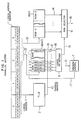
- Fig. 1 is a block diagram showing an intermediate stage prepared to explain the parallel access system according to the present invention.
- the logical address of a logical address register 1 is divided into two groups of bit positions, one of which groups consists of the bit positions (0, 1), (0, 2), ... (2, 2), and (2, 3) which are to be subject to address translation, while the other group consists of the bit positions (2, 4), (2, 5), ... (3, 6), and (3, 7) which are not subject to address translation.
- a TLB 2 is composed of pairs of logical addresses and physical addresses, so that upon reception of the address bits (0, 1) through (2, 3) to be subject to address translation from the logical address register 1 on a line 11, the TLB 2 puts out a physical address corresponding to the input logical address.
- a BAA 3 is a memory storing physical addresses of blocks of a BS 4 and constituted by four rows (row 0 - row 3), each row being constituted by four groups numbered with an address of two bits (2, 2) and (2, 3). According to this expression, it is possible to divide an address (32 bits) into four bytes (each 8 bits) from its MSB so as to specify the position of each bit by a format of (byte, bit).
- a comparator circuit 8 constituted by a plurality of comparators compares a physical address read out on lines 19 from the BAA 3 in response to the address input to the BAA 3 with a physical address obtained on a line 10 through address translation in the TLB 2, and upon detection of coincidence between both the physical addresses, the comparator circuit 8 makes a hit signal 18 be logic "1".
- a logical hit/decode circuit 5 checks the logical state of the output signal of the comparator circuit 8 and produces a row selection signal 15 which is in turn applied to a row selecting circuit 6.
- the logical hit/decode circuit 5 makes a synonym hit signal 9 be logic "1".
- a synonym control circuit 7 makes a synonym invalidation signal 17 be logic "1" so as to invalidate the valide bits of the synonym group by use of the row and group numbers.
- the BS 4 is constituted by four rows, and arranged to be accessed through a line 12 with the address bits "(2, 2), ... (3, 3)" to be subject to address translation through a line 12.
- the row selection circuit 6 selects one of the buffer row data 14 read out from the BS 4 and puts out a buffer data 16.
- U.S. Patent 4,332,010 concerns such an apparatus of the kind as described above.
- the data width required to a memory chip increases in proportion to the quantity of association and the memory cell reading current increases in proportion to the data width.
- the quantity of heat generation of the memory cell is therefore increased because it is given by a product of the current and voltage required for memory cell reading.
- BAA buffer address array
- BAA buffer address array
- BAA buffer address array
- the buffer control apparatus includes a first buffer address array (BAA) and a second buffer address array (BAA), the first buffer address array (BAA) being accessed with a part of bits of a logical address which are to be subject to address translation and a part of bits of a logical address which are not to be subject to address translation, the second buffer address array (BAA) being accessed or identified by use of a physical address and being capable of detecting a synonym.
- BAA buffer address array
- BAA buffer address array
- the function of the BAA is divided into a row selecting function, and a synonym group selecting function and the row selecting function and the synonym group selecting function are designed on corresponding memory chips respectively. That is, the function of the BAA is constituted by a combination of two kinds of buffer address arrays (BAAs) which will be described hereunder.
- BAAs buffer address arrays
- the first buffer address array (BAA) is constituted by columns having a quantity of association corresponding to the number of rows and being accessed with an address including bit portions of a logical address which are subject to address translation
- the second buffer address array (BAA) is constituted by columns having a quantity of association corresponding to a product of the number of rows and the number of groups and being accessed with an address including no bit portions of the logical address which are subject to address translation.
- the first buffer address array (BAA) is accessed every time the buffer memory is accessed so that the existence of a target block to be accessed in its logical group and a row of the buffer memory is selected.
- the second buffer address array (BAA) is accessed to judge whether or not the target block exists in its synonym group when the target block does not in the logical groups. When the target block exists in the synonym group, the synonym groups are invalidated in the first and second buffer address arrays (BAAs).
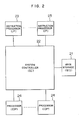
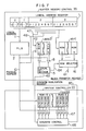
- Fig. 2 shows the structure of a general computer system which is constituted by a main storage (hereinafter abbreviated to “MS”) 21, a system controller (hereinafter abbreviated to “SC”) 22, instruction processors (hereinafter abbreviated to “iPs”) 23, and input/output processors (hereinafter abbreviated to “IOPs”) 24.
- the IOPs 24 is arranged to control the data transfer between the MS 21 and I/O devices.
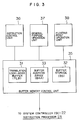
- Fig. 3 shows the structure of the iP 23.
- a buffer memory control unit 35 is connected to the SC 22 and supplies instructions and data to an instruction control unit 36, a general purpose operation unit 37, and a floating point operation unit 38.
- the buffer memory control unit 35 has a translation lookaside buffer (TLB) 31 for storing pairs of logical addresses and physical addresses, a buffer storage (BS) 32 for temporarily storing data read out from the MS 21, and a buffer address array (BAA) 33 having an array of addresses of the respective blocks of the BS 32 which are necessary to identify the BS 32.
- TLB translation lookaside buffer
- BS buffer storage
- BAA buffer address array
- the instruction control unit 36 reads out instructions from the BS 32, decodes the instructions and supplied the decoded instructions to the operation units 37 and 38.
- the general purpose operation unit 37 executes fixed point operation, logical operation, decimal operation, system control, and so on, and the floating point operation unit 38 executes floating point operation.
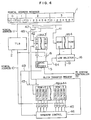
- Fig. 4 shows the internal structure of the buffer memory control unit 35, as an embodiment of the present invention.
- a logical address register 1 is arranged to latch a fetch request address sent out from the instruction control unit 36, the general purpose operation unit 37, and the floating point operation unit 38.
- the BAA 3 of Fig. 1 is divided into a logical buffer address array LBAA 3′ and a synonym buffer address array PBAA 44.
- the LBAA 3′ is arranged to be accessed with an address of bits (2, 2) through (3, 0) of a logical address including two bits (2, 2) and (2, 3) which are to be subject to address translation.
- a comparator circuit 8 constituted by a plurality of comparators compares a physical address put out from the LBAA 3′ with a physical address 10 translated in the TLB 2 to detect coincidence between the two physical addresses.
- a logical hit decode circuit 5 checks the output of the comparator circuit 8 and outs an output signal 64. Upon reception of the output signal 64 from the logical hit decode circuit 5, a row selecting circuit 16 selects row data (address) from the BS 4 so as to puts out a selected row data 61 when the data exists in the BS 4.
- the PBAA 44 is constituted by columns having a quantity of association corresponding to a product of the number of rows and the number of groups and being accessed with an address of five bits (2, 4) through (2, 7) and (3, 0) of the logic address which are not subject to address translation.
- the synonym groups are arranged in the direction of association and all the prospective ones of synonyms, that is, all the entries which may be synonyms, can be read out parallelly.
- a comparator circuit 45 constituted by a plurality of comparators compares the physical address 10 from the TLB 2 with the output from the PBAA 44. On the basis of the result of comparison by the comparator circuit 45, a synonym control circuit 46 puts out a hit row number and a hit synonym number.
- the LBAA 3′ is arranged to be accessed with an address of the logical address register 1 and a proper rows of the BS 4 is selected through the comparator circuit 8 and the logical hit decode circuit 5, so that the reading of the BS 4 is performed.
- Fig. 5 shows a second embodiment of the present invention which is different from the embodiment of Fig. 4 mainly in the structure of the physical buffer address array.
- a PBAA 53 is arranged to be accessed with a physical address 10 which has been obtained through the logical address to physical address translation by a TLB 2. In the entry of each row of the PBAA 53, the row number and group number corresponding to those of the LBAA 3′ are held.
- Fig. 7 shows a third embodiment of the present invention.
- a front address array (hereinafter abbreviated to "FAA") 66 is disposed in a system controller 22.
- the FAA 66 is a copy of a BAA provided for prevention of inconsistency of data between a plurality of buffers and memory locations in a structure of multiprocessor. That is, when writing is performed in one iP 23 (Fig. 2), the FAAs of all the iPs are identified, and if there is a block of a buffer holding the block in question, the block of the buffer is invalidated.
- the function of the PBAA 44 of Fig. 4 is realized in the FAA 66.
- a block transfer request 62 is generated.
- preparation is made for block transfer, access is made to the FAA 66, and existence of synonym is examined through a synonym control circuit 68.
- existence of synonym Upon detection of existence of synonym, a synonym invalidation request is sent out to the iP 23.
- the iP 23 Upon reception of the synonym invalidation request, the iP 23 resets the valid bit to thereby invalidate the synonym.
Landscapes
- Engineering & Computer Science (AREA)
- Theoretical Computer Science (AREA)
- Physics & Mathematics (AREA)
- General Engineering & Computer Science (AREA)
- General Physics & Mathematics (AREA)
- Memory System Of A Hierarchy Structure (AREA)
Applications Claiming Priority (2)
| Application Number | Priority Date | Filing Date | Title |
|---|---|---|---|
| JP247802/87 | 1987-10-02 | ||
| JP24780287 | 1987-10-02 |
Publications (3)
| Publication Number | Publication Date |
|---|---|
| EP0313857A2 true EP0313857A2 (de) | 1989-05-03 |
| EP0313857A3 EP0313857A3 (en) | 1989-05-10 |
| EP0313857B1 EP0313857B1 (de) | 1992-09-09 |
Family
ID=17168871
Family Applications (1)
| Application Number | Title | Priority Date | Filing Date |
|---|---|---|---|
| EP88116184A Expired - Lifetime EP0313857B1 (de) | 1987-10-02 | 1988-09-30 | Kontrolleinrichtung für Pufferspeicher |
Country Status (5)
| Country | Link |
|---|---|
| US (1) | US5109335A (de) |
| EP (1) | EP0313857B1 (de) |
| KR (1) | KR920001282B1 (de) |
| CA (1) | CA1304827C (de) |
| DE (1) | DE3874481T2 (de) |
Cited By (2)
| Publication number | Priority date | Publication date | Assignee | Title |
|---|---|---|---|---|
| EP0401021A3 (de) * | 1989-06-01 | 1992-03-11 | Fujitsu Limited | Pufferspeicheranordnung mit Adressen zur Seitenbezeichnung und seiteninternen Adressen |
| EP0439325A3 (en) * | 1990-01-22 | 1992-07-08 | Fujitsu Limited | A system for controlling an internally-installed cache memory |
Families Citing this family (13)
| Publication number | Priority date | Publication date | Assignee | Title |
|---|---|---|---|---|
| JPH0748191B2 (ja) * | 1989-08-10 | 1995-05-24 | 株式会社日立製作所 | バッファ記憶制御装置 |
| JPH0520197A (ja) * | 1991-07-09 | 1993-01-29 | Hitachi Ltd | 記憶管理システム及びマイクロプロセツサ |
| JPH0546475A (ja) * | 1991-08-15 | 1993-02-26 | Fujitsu Ltd | バツフア記憶制御方式 |
| US5412611A (en) * | 1992-03-17 | 1995-05-02 | Fujitsu, Limited | FIFO memory device capable of writing contiguous data into rows |
| JP2839060B2 (ja) * | 1992-03-02 | 1998-12-16 | インターナショナル・ビジネス・マシーンズ・コーポレイション | データ処理システムおよびデータ処理方法 |
| US5890221A (en) * | 1994-10-05 | 1999-03-30 | International Business Machines Corporation | Method and system for offset miss sequence handling in a data cache array having multiple content addressable field per cache line utilizing an MRU bit |
| US6006312A (en) * | 1995-02-27 | 1999-12-21 | Sun Microsystems, Inc. | Cachability attributes of virtual addresses for optimizing performance of virtually and physically indexed caches in maintaining multiply aliased physical addresses |
| US5680566A (en) * | 1995-03-03 | 1997-10-21 | Hal Computer Systems, Inc. | Lookaside buffer for inputting multiple address translations in a computer system |
| US5956754A (en) * | 1997-03-03 | 1999-09-21 | Data General Corporation | Dynamic shared user-mode mapping of shared memory |
| US6807615B1 (en) * | 1999-04-08 | 2004-10-19 | Sun Microsystems, Inc. | Apparatus and method for providing a cyclic buffer using logical blocks |
| GB2372589B (en) * | 2001-02-21 | 2003-01-22 | 3Com Corp | Memory aliasing in a processor system |
| US7206916B2 (en) * | 2004-03-08 | 2007-04-17 | Sun Microsystems, Inc. | Partial address compares stored in translation lookaside buffer |
| CN113934655B (zh) * | 2021-12-17 | 2022-03-11 | 北京微核芯科技有限公司 | 解决高速缓冲存储器地址二义性问题的方法和装置 |
Family Cites Families (8)
| Publication number | Priority date | Publication date | Assignee | Title |
|---|---|---|---|---|
| JPS5440182B2 (de) * | 1974-02-26 | 1979-12-01 | ||
| US4332010A (en) * | 1980-03-17 | 1982-05-25 | International Business Machines Corporation | Cache synonym detection and handling mechanism |
| DE3177181D1 (de) * | 1980-11-10 | 1990-06-21 | Ibm | Anordnung zur erkennung und verarbeitung von synonymen in cache-speichern. |
| JPS5948879A (ja) * | 1982-09-10 | 1984-03-21 | Hitachi Ltd | 記憶制御方式 |
| JPS6093563A (ja) * | 1983-10-27 | 1985-05-25 | Hitachi Ltd | バツフア記憶制御方式 |
| JPS62118457A (ja) * | 1985-11-19 | 1987-05-29 | Hitachi Ltd | バツフア記憶制御方式 |
| US4693800A (en) * | 1985-11-29 | 1987-09-15 | The B. F. Goodrich Company | Property variation of dispersion resins by electrofiltration |
| JPH0661066B2 (ja) * | 1986-10-20 | 1994-08-10 | 株式会社日立製作所 | 記憶制御装置 |
-
1988
- 1988-09-28 KR KR1019880012533A patent/KR920001282B1/ko not_active Expired
- 1988-09-29 US US07/250,942 patent/US5109335A/en not_active Expired - Fee Related
- 1988-09-29 CA CA000578896A patent/CA1304827C/en not_active Expired - Lifetime
- 1988-09-30 DE DE8888116184T patent/DE3874481T2/de not_active Expired - Fee Related
- 1988-09-30 EP EP88116184A patent/EP0313857B1/de not_active Expired - Lifetime
Cited By (4)
| Publication number | Priority date | Publication date | Assignee | Title |
|---|---|---|---|---|
| EP0401021A3 (de) * | 1989-06-01 | 1992-03-11 | Fujitsu Limited | Pufferspeicheranordnung mit Adressen zur Seitenbezeichnung und seiteninternen Adressen |
| US5544293A (en) * | 1989-06-01 | 1996-08-06 | Fujitsu Limited | Buffer storage system and method using page designating address and intra-page address and detecting valid data |
| EP0439325A3 (en) * | 1990-01-22 | 1992-07-08 | Fujitsu Limited | A system for controlling an internally-installed cache memory |
| US5517633A (en) * | 1990-01-22 | 1996-05-14 | Fujitsu Limited | System for controlling an internally-installed cache memory |
Also Published As
| Publication number | Publication date |
|---|---|
| KR890007170A (ko) | 1989-06-19 |
| CA1304827C (en) | 1992-07-07 |
| DE3874481T2 (de) | 1993-01-28 |
| KR920001282B1 (ko) | 1992-02-10 |
| EP0313857A3 (en) | 1989-05-10 |
| DE3874481D1 (de) | 1992-10-15 |
| US5109335A (en) | 1992-04-28 |
| EP0313857B1 (de) | 1992-09-09 |
Similar Documents
| Publication | Publication Date | Title |
|---|---|---|
| US5133058A (en) | Page-tagging translation look-aside buffer for a computer memory system | |
| EP0095033B1 (de) | Teilassoziativer Sektorpufferspeicher | |
| KR920005280B1 (ko) | 고속 캐쉬 시스템 | |
| US5426750A (en) | Translation lookaside buffer apparatus and method with input/output entries, page table entries and page table pointers | |
| US3618040A (en) | Memory control apparatus in multiprocessor system | |
| EP0090575B1 (de) | Speicheranordnung | |
| EP0313857B1 (de) | Kontrolleinrichtung für Pufferspeicher | |
| US4916604A (en) | Cache storage apparatus | |
| CA2022529C (en) | Apparatus for page tagging in a computer system | |
| EP0149389B1 (de) | Anordnung zur Adressumsetzungssteuerung | |
| EP0243724A2 (de) | Mehrebenen-Speicherhierarchie mit variabler Adressierungsart | |
| US6571316B1 (en) | Cache memory array for multiple address spaces | |
| EP0303648B1 (de) | Zentralprozessoreinheit für digitale datenverarbeitungsanordnung mit cache-speicherverwaltungsvorrichtung | |
| EP0365117B1 (de) | Datenverarbeitungsvorrichtung mit Cache-Speicher | |
| EP0103132A2 (de) | Pufferspeichersteuerungsanordnung | |
| EP0468804A2 (de) | Steuerungsanordnung eines hierarchischen Speichers | |
| US5603008A (en) | Computer system having cache memories with independently validated keys in the TLB | |
| EP0519685A1 (de) | Adressenübersetzung | |
| US4920536A (en) | Error recovery scheme for destaging cache data in a multi-memory system | |
| CN1003680B (zh) | 可用实地址及虚地址寻址的高速缓冲存贮器 | |
| EP0153109B1 (de) | Cache-Kohärenz-Anordnung | |
| JP2675836B2 (ja) | データ処理装置 | |
| US6253301B1 (en) | Method and apparatus for a dedicated physically indexed copy of the data cache tag arrays | |
| GB2037466A (en) | Computer with cache memory | |
| US6493792B1 (en) | Mechanism for broadside reads of CAM structures |
Legal Events
| Date | Code | Title | Description |
|---|---|---|---|
| PUAI | Public reference made under article 153(3) epc to a published international application that has entered the european phase |
Free format text: ORIGINAL CODE: 0009012 |
|
| PUAL | Search report despatched |
Free format text: ORIGINAL CODE: 0009013 |
|
| AK | Designated contracting states |
Kind code of ref document: A2 Designated state(s): DE FR GB |
|
| AK | Designated contracting states |
Kind code of ref document: A3 Designated state(s): DE FR GB |
|
| 17P | Request for examination filed |
Effective date: 19890417 |
|
| 17Q | First examination report despatched |
Effective date: 19910325 |
|
| GRAA | (expected) grant |
Free format text: ORIGINAL CODE: 0009210 |
|
| AK | Designated contracting states |
Kind code of ref document: B1 Designated state(s): DE FR GB |
|
| REF | Corresponds to: |
Ref document number: 3874481 Country of ref document: DE Date of ref document: 19921015 |
|
| ET | Fr: translation filed | ||
| PLBE | No opposition filed within time limit |
Free format text: ORIGINAL CODE: 0009261 |
|
| STAA | Information on the status of an ep patent application or granted ep patent |
Free format text: STATUS: NO OPPOSITION FILED WITHIN TIME LIMIT |
|
| 26N | No opposition filed | ||
| PGFP | Annual fee paid to national office [announced via postgrant information from national office to epo] |
Ref country code: FR Payment date: 20010717 Year of fee payment: 14 |
|
| PGFP | Annual fee paid to national office [announced via postgrant information from national office to epo] |
Ref country code: GB Payment date: 20010920 Year of fee payment: 14 |
|
| PGFP | Annual fee paid to national office [announced via postgrant information from national office to epo] |
Ref country code: DE Payment date: 20011129 Year of fee payment: 14 |
|
| REG | Reference to a national code |
Ref country code: GB Ref legal event code: IF02 |
|
| PG25 | Lapsed in a contracting state [announced via postgrant information from national office to epo] |
Ref country code: GB Free format text: LAPSE BECAUSE OF NON-PAYMENT OF DUE FEES Effective date: 20020930 |
|
| PG25 | Lapsed in a contracting state [announced via postgrant information from national office to epo] |
Ref country code: DE Free format text: LAPSE BECAUSE OF NON-PAYMENT OF DUE FEES Effective date: 20030401 |
|
| GBPC | Gb: european patent ceased through non-payment of renewal fee |
Effective date: 20020930 |
|
| PG25 | Lapsed in a contracting state [announced via postgrant information from national office to epo] |
Ref country code: FR Free format text: LAPSE BECAUSE OF NON-PAYMENT OF DUE FEES Effective date: 20030603 |
|
| REG | Reference to a national code |
Ref country code: FR Ref legal event code: ST |