EP0314227A2 - Breitbandiger unsymmetrischer Spannungs-Strom-Wandler und Verstärkungsregelungsschaltung - Google Patents
Breitbandiger unsymmetrischer Spannungs-Strom-Wandler und Verstärkungsregelungsschaltung Download PDFInfo
- Publication number
- EP0314227A2 EP0314227A2 EP88202286A EP88202286A EP0314227A2 EP 0314227 A2 EP0314227 A2 EP 0314227A2 EP 88202286 A EP88202286 A EP 88202286A EP 88202286 A EP88202286 A EP 88202286A EP 0314227 A2 EP0314227 A2 EP 0314227A2
- Authority
- EP
- European Patent Office
- Prior art keywords
- input
- signal
- circuit
- amplifier
- current
- Prior art date
- Legal status (The legal status is an assumption and is not a legal conclusion. Google has not performed a legal analysis and makes no representation as to the accuracy of the status listed.)
- Withdrawn
Links
- 239000000872 buffer Substances 0.000 description 34
- 238000010586 diagram Methods 0.000 description 14
- 239000000543 intermediate Substances 0.000 description 5
- 238000000034 method Methods 0.000 description 5
- 230000007850 degeneration Effects 0.000 description 2
- 230000000694 effects Effects 0.000 description 2
- 239000003990 capacitor Substances 0.000 description 1
- 230000000295 complement effect Effects 0.000 description 1
- 239000002131 composite material Substances 0.000 description 1
- 238000010276 construction Methods 0.000 description 1
- 230000008878 coupling Effects 0.000 description 1
- 238000010168 coupling process Methods 0.000 description 1
- 238000005859 coupling reaction Methods 0.000 description 1
- 102220098914 rs36097930 Human genes 0.000 description 1
- 102220037287 rs387906970 Human genes 0.000 description 1
Images


Classifications
-
- H—ELECTRICITY
- H03—ELECTRONIC CIRCUITRY
- H03G—CONTROL OF AMPLIFICATION
- H03G3/00—Gain control in amplifiers or frequency changers
-
- H—ELECTRICITY
- H03—ELECTRONIC CIRCUITRY
- H03F—AMPLIFIERS
- H03F1/00—Details of amplifiers with only discharge tubes, only semiconductor devices or only unspecified devices as amplifying elements
- H03F1/30—Modifications of amplifiers to reduce influence of variations of temperature or supply voltage or other physical parameters
- H03F1/302—Modifications of amplifiers to reduce influence of variations of temperature or supply voltage or other physical parameters in bipolar transistor amplifiers
-
- G—PHYSICS
- G05—CONTROLLING; REGULATING
- G05F—SYSTEMS FOR REGULATING ELECTRIC OR MAGNETIC VARIABLES
- G05F1/00—Automatic systems in which deviations of an electric quantity from one or more predetermined values are detected at the output of the system and fed back to a device within the system to restore the detected quantity to its predetermined value or values, i.e. retroactive systems
- G05F1/10—Regulating voltage or current
- G05F1/46—Regulating voltage or current wherein the variable actually regulated by the final control device is DC
- G05F1/56—Regulating voltage or current wherein the variable actually regulated by the final control device is DC using semiconductor devices in series with the load as final control devices
- G05F1/561—Voltage to current converters
-
- G—PHYSICS
- G05—CONTROLLING; REGULATING
- G05F—SYSTEMS FOR REGULATING ELECTRIC OR MAGNETIC VARIABLES
- G05F3/00—Non-retroactive systems for regulating electric variables by using an uncontrolled element, or an uncontrolled combination of elements, such element or such combination having self-regulating properties
- G05F3/02—Regulating voltage or current
- G05F3/08—Regulating voltage or current wherein the variable is DC
- G05F3/10—Regulating voltage or current wherein the variable is DC using uncontrolled devices with non-linear characteristics
- G05F3/16—Regulating voltage or current wherein the variable is DC using uncontrolled devices with non-linear characteristics being semiconductor devices
- G05F3/20—Regulating voltage or current wherein the variable is DC using uncontrolled devices with non-linear characteristics being semiconductor devices using diode- transistor combinations
- G05F3/22—Regulating voltage or current wherein the variable is DC using uncontrolled devices with non-linear characteristics being semiconductor devices using diode- transistor combinations wherein the transistors are of the bipolar type only
-
- H—ELECTRICITY
- H03—ELECTRONIC CIRCUITRY
- H03G—CONTROL OF AMPLIFICATION
- H03G1/00—Details of arrangements for controlling amplification
- H03G1/04—Modifications of control circuit to reduce distortion caused by control
Definitions
- This invention relates to a wideband, DC coupled amplifier comprising: an input terminal for receiving an input signal; an output terminal for providing an output signal; a first amplifier stage having an input lead connected to said input terminal for receiving said input signal and providing a first intermediate signal having a first component which is a function of said input signal and having a second component which is a function of one or more bias signals used in said first amplifier stage
- Wide bandwidth amplifiers are used to amplify video signals.
- Such wide-band amplifiers are described, for example, in "A New Wide-Band Amplifier Technique” Barrie Gilbert, IEEE Journal of Solid-State Circuits, Vol. SC-3, pages 353-365, December 1968; "Design Techniques for Monolithic Operational Amplifiers", Robert J. Widlar, IEEE Journal of Solid-State Circuits, Vol. SC-4, No.4, page 184-191, August 1969; “Amplifying Devices and Low-Pass Amplifier Design", John Wiley & Sons, 1968; and United States Patent No.3,849,735 issued November 19, 1974 to Haenen et al , and assigned to U.S. Philips Corporation.
- wide bandwidth amplifiers typically require response down to DC, thereby precluding AC coupling.
- Video standards used throughout the world require video signals to be referenced to ground, thereby requiring the use of wide bandwidth, single ended amplifiers.
- the prior art has not provided a wideband, single ended, DC coupled monolithic amplifier suitable for use, for example, with video signals.
- a novel wideband, DC coupled, single-ended voltage-to-current converter and gain control circuit is provided.
- the circuit of this invention is designed to receive an input signal referenced to ground such that for zero input signal, zero output signal is provided.
- the circuit of this invention provides a linear output current in response to the input voltage.
- a circuit is provided which allows for the input of a signal, typically a wide-band signal, such as a video signal, in any one of a desired number of formats, such as ECL, TTL, or analog.
- Contrast and brightness signals are also applied as input signals to the circuit, which combines the desired one of the wideband information, contrast, and brightness signals in order to provide a suitable output signal.
- the input data is a video signal
- the output signal is a current suitable for driving a CRT display.
- a replica bias circuit which allows the output signal to be a function of the input signal without offsets introduced by bias currents used throughout the circuit.
- An amplifier as defined in the first paragraph is, according to the invention, characterized in that the wideband, DC coupled amplifier further comprises: a replica bias circuit for generating a replica bias signal which is related to and tracks said second component of said first intermediate signal; means for combining said first intermediate signal and said replica bias signal to provide a second intermediate signal which is a function of said input signal and not a function of said bias signals or said replica bias signal; and a second amplifier stage having an input lead for receiving said second intermediate signal and having an output lead connected to said output terminal for providing said output signal, said output signal being a function of said input signal and not a function of said bias signals or said replica bias signal.
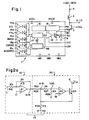
- Fig. 1 is a block diagram of one embodiment of a circuit 1 constructed in accordance with the teachings of this invention which serves as a transconductance amplifier which receives a digital or composite video input signal (with sync removed) and controls a CRT (not shown) via CRT drive transistor 2.
- this invention is suitable for other applications, for example, in other wide-band applications, or in any application where it is desired to construct an amplifier whose output signal is a function of the input signal without components caused by bias currents used in the amplifier itself.
- circuit 1 receives input signals related to a video signal and provides an output signal suitable for driving a CRT display using external power transistor 2 together with inductor 3 and load resistor 4.
- circuit 1 includes input buffer 14a suitable for receiving an ECL signal defining the video pattern to be displayed.
- the video pattern is provided in TTL format and supplied to input buffer 14b.
- the video information is an analog signal which is applied to analog video input buffer 15a.
- Circuit 1 also includes input buffers 15b and 15c for receiving contrast and brightness information, respectively.
- Any suitable ECL input buffer may be used for buffer 14a, such as those well known in the prior art.
- any suitable TTL input buffer can be used for input buffer 14b, such as those well known in the prior art.
- Buffers 15a through 15c may advantageously be constructed in accordance with the teachings of this invention to provide wideband transconductance amplifiers, particularly having a minimum -3 dB bandwidth of approximately 200 MHz, and are described in more detail later.
- the output current of brightness amplifier 15c provides a fixed DC current offset which is applied to the input lead of output amplifier 19.
- the output current of one of ECL input buffer 14a, TTL input buffer 14b, or analog input buffer 15a is selected as the video input signal to gain control circuit 17.
- the current from contrast input amplifier 15b is also provided to an input lead of gain control circuit 17, and varies the gain of gain control circuit 17 linearly from 0 to 120 mA/V, for an input contrast signal of 0 to 3 volts.
- Output stage 19 is a biasing amplifier with current feedback which linearizes the output signal and makes circuit 1 independent of the current gain (beta) of external output transistor 2.
- Circuit 1 also includes I/V reference 16 which serves to provide voltage and current reference levels for use throughout circuit 1.
- I/V reference 16 serves to provide voltage and current reference levels for use throughout circuit 1.
- Biasing circuits of this nature are well known in the art, and are described, for example, in the previously referenced text by Gray and Meyer, and in U.S. Patents 3,430,155 and 4,061,959. Of course, any suitable current and voltage reference level circuits can be utilized to form I/V reference 16.
- Circuit 1 also includes gain control circuit 17 which serves to receive the analog information in the form of a current from a selected one of analog input buffers 14a, 14b, or 15a, in response to the ECL, TTL, or analog input signal or voltages, respectively.
- the output current I ECL from ECL input amplifier 14a or the output current I TTL from TTL input amplifier 14b can be used in place of I analog , depending on the type of input information provided. When one source of video information is selected, the input leads of the others are grounded. If not, undesired input signals will be combined with the desired video information and may saturate gain control circuit 17.
- gain control circuit 17 provides output current I drive to the input lead of output amplifier 19, which current is summed with the output current from brightness amplifier 15c.
- Output amplifier 19 amplifies this summed current to provide an amplified current to drive power transistor 19a, which in turn provides an output current IOUT to the emitter of power transistor 2. It has been found that it is convenient to form power transistor 19a within the same integrated circuit containing those components located within the box in Fig.1, while forming power transistor 2, inductor 3, and resistor 4 as components external to the integrated circuit.
- the intensity of the beam of electrons appearing on the CRT screen (not shown) is controlled by the voltage on the collector of transistor 2, which is applied to the CRT.
- This voltage is determined by current IOUT, the values of inductor 3 and resistor 4, and the input capacitance of the CRT.
- current IOUT current IOUT
- inductor 3 and resistor 4 current IOUT
- inductor 3 and resistor 4 current IOUT
- Circuit 1 also receives an IDLE input signal which controls an IDLE current source 6 which provides a minimum DC current value (typically approximately 1.8 mA) for IOUT, thereby preventing power transistor 2 from turning off, thereby eliminating turn-on delay of power transistor 2.
- an IDLE current source 6 which provides a minimum DC current value (typically approximately 1.8 mA) for IOUT, thereby preventing power transistor 2 from turning off, thereby eliminating turn-on delay of power transistor 2.
- Circuit 1 also receives a SHUT signal which is applied to disable amplifier 19, in essence to blank the CRT screen. With amplifier 19 disabled by the SHUT signal, IDLE current source 6 provides the minimum DC current for IOUT, but insufficient current to light the CRT screen.
- Circuit 1 also includes a COMP lead which allows a compensation capacitor to be connected between the input lead of output amplifier 19 and ground in order to reduce the bandwidth of output amplifier 19, if desired. For example, in one embodiment, connecting a capacitance of approximately 100 pF between the COMP lead and ground provides a -3 dB bandwidth of approximately 30 MHz.
- Output amplifier 19 may be constructed, for example, as taught in the previously described reference by Gray and Meyer.
- Circuit 1 also includes protection subcircuit 18 including leads PR1 and PR2 which allow resistors to be connected between leads PR1 or PR2 and ground, thereby setting a maximum output current limit from output amplifier 19, which limits the maximum level of current IOUT.
- Protection circuit 18 includes leads PR1 and PR2 which allow resistors to be connected between leads PR1 or PR2 and ground, thereby setting a maximum output current limit from output amplifier 19, which limits the maximum level of current IOUT. Circuits suitable for use as protection circuit 18 are known in the prior art and are taught, for example, in the previously described reference by Gray and Meyer.
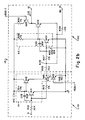
- Fig. 2a shows a schematic diagram of one embodiment of voltage-to-current converter 15 constructed in accordance with the teachings of this invention suitable for use as input amplifiers 15a, 15b, or 15c of Fig.1.
- Voltage-to-current converter 15 includes two subsections, inverting amplifier 10 and unity gain buffer 20.
- Inverting amplifier 10 receives an input signal on terminal 11 (which is, for example, the ANALOG video input signal applied to input buffer 15a, or the CONTRAST input signal applied to input buffer 15b, or the BRIGHTNESS input signal applied to input buffer 15c of Fig.1).Amplifier A1 in conjunction with resistors R12 and R13 provide a gain of approximately -1/6, with a DC bias of 7/6 V be (Q11), where Q11 is the inverting input transistor (Fig. 2b) of amplifier A1. Naturally, any desired gain, as determined by the ratio of resistance of resistors R12 and R13, and any DC bias, can be used in accordance with the teachings of this invention.
- V N18 the voltage on output node N18 of amplifier A1
- V be (Q11) the base-emitter voltage of inverting input transistor Q11 (Fig. 1b) of amplifier A1
- V in the input voltage on input terminal 11
- the output signal from amplifier A1 is applied to input resistor R26 of unity gain buffer 20.
- Unity gain buffer 20 includes amplifier A2 and resistors R26, R27, R29, and output transistor Q24, in order to provide output current I15 available at terminal 12 in response to the input voltage received from inverting amplifier 10.
- Resistors R27 and R29 are selected to provide a voltage divider having a ratio of 6/7 in order to complement the 1/6 voltage ratio provided by inverting amplifier 10.
- Unity gain buffer 20 also includes resistor R38 (which in one embodiment has a value of 12K ohms) connected between the emitter of output transistor Q24 and terminal 13. Terminal 13 receives a replica bias voltage in order to DC bias input node N19, which in turn biases the base of transistor Q24 to the voltage at node N19 plus V be .
- resistor R38 which in one embodiment has a value of 12K ohms
- V N19 the voltage on node 18
- V N19 the voltage on node 19
- V N20 the voltage on node 20
- V RB the replica bias voltage on terminal 13
- the voltage drop across R38 is equal to V be .
- VN19 7 6 V be (Q11) ;
- a novel, single ended, DC coupled amplifier is provided which is capable of providing an output current I15 which is directly related to the input voltage V in , without any effect of the bias voltage used in the circuit.
- Fig. 2b is a more detailed schematic diagram of one embodiment of the circuit of Fig. 2a.
- amplifier A1 includes current source transistor Q13 and emitter degeneration resistor R15.
- Transistor Q13 receives a constant DC bias voltage VBIAS-1 from I/V reference circuit 16 (Fig. 1), as is well known to those of ordinary skill in the art, in order to properly bias transistor Q13 to provide a constant collector current I13.
- transistor Q25 which is provided as a current source having its collector connected to output node 12, and its emitter connected to emitter degeneration resistor R30.
- the base of PNP transistor Q25 is biased by an external bias voltage VBIAS-2, which is provided by I/V reference block 16 of Fig.1 in order to properly bias transistor Q25 to provide a constant current.
- VBIAS-2 external bias voltage
- transistor Q24 when transistor Q24 is conducting, the current provided by transistor Q25 is consumed by transistor Q24, and transistor Q24 also sinks current I15 from terminal 12.
- transistor Q24 turned off, the current supplied by current source transistor Q25 serves as a -I15 current available on terminal 12.Due to the construction of the embodiment of Fig.
- terminal 12 can drive external circuitry (not shown) having voltage levels greater than or equal to about 2 V be without causing transistor Q24 to saturate.
- VBIAS-2 is selected to be approximately 1 volt below VCC.
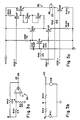
- Fig. 3a is a schematic diagram of one embodiment of a replica bias circuit 99 constructed in accordance with the teachings of this invention.
- Replica bias circuit 99 includes amplifier A5, and biasing and feedback resistors R40, R41, and R42.
- V A is the voltage on the inverting input lead of amplifier A5
- V A V be (Q31)
- V be (Q31) V be (Q11)
- transistors Q31 and Q11 are matched.
- Fig. 3c is a more detailed schematic diagram of one embodiment of a replica bias circuit 99 suitable for use in accordance with the teachings of this invention.
- Replica bias circuit 99 serves to provide a replica bias output voltage on terminal 23 for use in DC biasing node N19 of unity gain buffer 20 of Fig. 2a, which serves as portion of the analog, contrast, and brightness input buffers 15a, 15b, and 15c, respectively, of Fig. 1.
- Replica bias circuit 99 uses the bias voltage levels VBIAS-2, VBIAS-3 and VBIAS-4 from I/V Reference 16 (Fig.1). Conveniently, these bias voltages are also used by the embodiment of amplifier 15 of Fig. 2b, and the embodiment of gain control circuit 17 of Fig. 4b, although any source of suitable bias voltages can be used for each of those circuits. It is not important that they are biased from the same levels.
- VBIAS-2, VBIAS-3, and VBIAS-4 are derived in a well known manner from I/V reference 16 of Fig. 1.
- VBIAS-2 is typically approximately VCC - 1 volt, and serves to bias PNP transistor Q127.
- VBIAS-3 and VBIAS-4 are approximately equal and serve to bias NPN transistors Q125 and Q126, respectively.
- Replica bias circuit 99 provides a replica bias signal on output terminal 23 which serves to bias analog amplifier 15a, contrast amplifier 15b, and brightness amplifier 15c.
- Replica bias serves to cause the biasing, and thus the gain, of analog amplifier 15a, contrast amplifier 15b, and brightness amplifier 15c to track in response to any changes in V be due to, for example, VCC.
- each of the analog, contrast and brightness amplifiers derive DC bias for their node 19 from the replica bias voltage available on terminal 23. Since, in this embodiment, three separate input amplifiers 15a, 15b, and 15c are receiving the same replica bias voltage in order to remove the effects on their transfer function due to bias voltages, input transistors Q11 and Q23 (amplifier 15 of Fig. 2b) and transistor Q31 (amplifier A3 of the replica bias circuitry of Fig. 3c) are very closely matched. Of importance, it is not necessary that each input amplifier 15a, 15b, 15c (Fig.1) receives a replica bias voltage from the same source, as it is not particularly important that input amplifiers 15a, 15b, and 15c track each other. What is important is that a given replica bias signal properly track changes in V be for a particular amplifier or amplifiers which are being influenced by that replica bias signal.
- FIG. 4a is a schematic diagram of one embodiment 6 of gain control circuit 17 (Fig.1) which functions as a current multiplier.
- I contrast and I analog serve as input currents to gain control circuit 17.
- Transistor Q36 receives on its base bias voltage VBIAS-6 (typically approximately 4V be ) where V be here represents the standard base-emitter voltage of a forward biased bipolar transistor, in order to provide a desired DC bias on the input lead of unity gain buffer A3. Therefore, the output voltage on the output lead of unity gain buffer A3 is provided in response to the voltage appearing on the input lead of unity gain buffer A3, as determined by the bias set by transistor Q36 and the I contrast current.
- VBIAS-6 typically approximately 4V be
- V be represents the standard base-emitter voltage of a forward biased bipolar transistor
- V IN (A3) (VBIAS-6) - V be (Q36) (12)
- V be (Qx) V T ln(I C (Qx)/I S (Qx);
- I C (Qx) the collector current of transistor Qx
- I S (Qx) the saturation current of transistor Qx
- V T kT/q
- k Bolrtzman's constant
- T temperature in degrees Kelvon
- q the charge of an electron.
- Transistor Q41 operates in a similar fashion as transistor Q36, except that its base voltage is provided by the output lead of unity gain buffer A3 in response to V IN (A3).
- output voltage V OUT (A4) on the output lead of unity gain buffer A4 is a function of both I contrast and I analog .
- Transistor Q49 receives its base drive from VBIAS-6 (4V be ), and is biased by the collector of transistor Q46.
- the emitters of transistors Q46 and Q47 are connected to current source 32 controlled by VBIAS-3.
- VBIAS-3 is also conveniently used to control current source 31 which provides current I1 to the emitter of transistor Q48, which in turn drives the base of transistor Q47.
- V be (Q36) + V be (Q41) + V be (Q46) -V be (Q47) - V be (Q48) - V be (Q49) 0 (21)
- transistor Q47 provides on its collector an output current I drive in response to the output voltage on the output lead of unity gain buffer A4:
- I drive the output drive current provided by gain control circuit 17;
- I1 a reference current; and
- K a constant determined by the ratio of transistor saturation currents: Since the saturation current of a bipolar transistor is proportional to the area of its emitter,
- I contrast 600 ⁇ A
- I drive 3 I analog (28)
- VBIAS-3 is a highly stable voltage thereby causing I drive to be highly stable with respect to the voltage on output lead of unity gain buffer 19.
- VBIAS-3 In order for the transfer function of output amplifier 17 to be a function of only I contrast and I analog , VBIAS-3, and thus reference current I1 , is made to be highly constant.
- Unity gain buffers A3 and A4 serve to maintain the low output impedance normally seen by the base of transistors Q41 and Q46 from emitter followers Q36 and Q41, respectively. In this manner, transistors Q41 and Q46 are always driven by a low source impedance, thereby insuring high frequency linearity.
- Fg. 4b is a more detailed schematic diagram of one embodiment of gain control circuit 17 shown in Fig. 4a.
- Amplifiers A3 and A4 are shown in more detail, and their current sources Q78 and Q80 are driven by VBIAS-4. However, current sources Q65 and Q64 are driven by a separate bias voltage VBIAS-2. Of importance, transistors Q65 and 64 are operated by a bias voltage VBIAS-2, rather than being internally biased within unity gain buffers A3 and A4 respectively. This serves to reduce the amount of current source base drive required to be derived from a particular voltage regulator, and also minimizes high frequency feedback within each amplifier A3 and A4.
- the VBIAS-6 voltage applied to the bases of transistors A36, Q175, Q77, and Q49 is set at 4V be by transistors Q69 through Q72.
- the base of transistor Q69 is driven by a bias current IBIAS equal to 2 times the reference current of 200 microamps.
- VBIAS-3 is provided by transistors A73 and Q74 which receive a bias current IBIAS equal to 3 times the reference current or aproximately 600 microamps. This VBIAS-3 is also used to drive transistor Q89, which is part of the biasing network consisting of transistors Q69 through Q72. VBIAS-3 also drive the bases of transistors A53 and Q52, which in turn drive the emitters of transistors Q46, Q47 and transistor Q48, respectively, as previously described with regard to Fig. 4a. Transistor Q86 is driven by VBIAS-3 and in turn biases Q88 in order to provide VBIAS-2.
- VBIAS-2 biases the base of transistor Q60, which establishes, in conjunction with transistors Q81, Q85, Q39 and Q59, VBIAS-4, as previously described.
- VBIAS-4 in turn drives the bases of current sources Q78, Q79, Q80 and Q54.
- a novel, wide band, DC coupled, single ended voltage-to-current converter which receives a bias voltage from the replica bias circuit, thereby causing the amplifier to have a transfer function independent of the bias levels used in the amplifier.
Landscapes
- Engineering & Computer Science (AREA)
- Physics & Mathematics (AREA)
- Electromagnetism (AREA)
- General Physics & Mathematics (AREA)
- Radar, Positioning & Navigation (AREA)
- Automation & Control Theory (AREA)
- Microelectronics & Electronic Packaging (AREA)
- Nonlinear Science (AREA)
- Power Engineering (AREA)
- Amplifiers (AREA)
- Control Of Amplification And Gain Control (AREA)
Applications Claiming Priority (2)
| Application Number | Priority Date | Filing Date | Title |
|---|---|---|---|
| US11513687A | 1987-10-30 | 1987-10-30 | |
| US115136 | 1987-10-30 |
Publications (2)
| Publication Number | Publication Date |
|---|---|
| EP0314227A2 true EP0314227A2 (de) | 1989-05-03 |
| EP0314227A3 EP0314227A3 (de) | 1991-03-20 |
Family
ID=22359499
Family Applications (1)
| Application Number | Title | Priority Date | Filing Date |
|---|---|---|---|
| EP19880202286 Withdrawn EP0314227A3 (de) | 1987-10-30 | 1988-10-13 | Breitbandiger unsymmetrischer Spannungs-Strom-Wandler und Verstärkungsregelungsschaltung |
Country Status (3)
| Country | Link |
|---|---|
| EP (1) | EP0314227A3 (de) |
| JP (1) | JPH02126709A (de) |
| KR (1) | KR890007495A (de) |
Cited By (2)
| Publication number | Priority date | Publication date | Assignee | Title |
|---|---|---|---|---|
| EP0463857A1 (de) * | 1990-06-25 | 1992-01-02 | Nec Corporation | Emittergeerdete Verstärkerschaltung mit Vorspannungsschaltung |
| EP1615143A3 (de) * | 2004-06-30 | 2008-01-23 | Fujitsu Limited | Operationsgerät und Kontrollverfahren |
Family Cites Families (3)
| Publication number | Priority date | Publication date | Assignee | Title |
|---|---|---|---|---|
| JPS5612050B2 (de) * | 1974-05-30 | 1981-03-18 | ||
| JPS5165861A (en) * | 1974-12-05 | 1976-06-07 | Sony Corp | Toranjisutano baiasukairo |
| US4450367A (en) * | 1981-12-14 | 1984-05-22 | Motorola, Inc. | Delta VBE bias current reference circuit |
-
1988
- 1988-10-13 EP EP19880202286 patent/EP0314227A3/de not_active Withdrawn
- 1988-10-27 JP JP63271912A patent/JPH02126709A/ja active Pending
- 1988-10-27 KR KR1019880014005A patent/KR890007495A/ko not_active Withdrawn
Cited By (4)
| Publication number | Priority date | Publication date | Assignee | Title |
|---|---|---|---|---|
| EP0463857A1 (de) * | 1990-06-25 | 1992-01-02 | Nec Corporation | Emittergeerdete Verstärkerschaltung mit Vorspannungsschaltung |
| EP1615143A3 (de) * | 2004-06-30 | 2008-01-23 | Fujitsu Limited | Operationsgerät und Kontrollverfahren |
| EP2116938A1 (de) * | 2004-06-30 | 2009-11-11 | Fujitsu Limited | Operationsgerät und Kontrollverfahren |
| US7822888B2 (en) | 2004-06-30 | 2010-10-26 | Fujitsu Limited | Data buffer control which controls selection of path and operation of data buffer, based on stored configuration information |
Also Published As
| Publication number | Publication date |
|---|---|
| EP0314227A3 (de) | 1991-03-20 |
| KR890007495A (ko) | 1989-06-20 |
| JPH02126709A (ja) | 1990-05-15 |
Similar Documents
| Publication | Publication Date | Title |
|---|---|---|
| US6111463A (en) | Operational transconductance amplifier and multiplier | |
| US6172555B1 (en) | Bandgap voltage reference circuit | |
| KR20010020410A (ko) | 선형성 및 대역폭이 개선된 가변 이득 증폭기 | |
| JPS6354006A (ja) | 電流ミラ−回路 | |
| JP3119215B2 (ja) | 差動アンプ | |
| US5107224A (en) | Wideband single-ended voltage-to-current converter and gain-control circuit | |
| EP0387951B1 (de) | Stromverstärker | |
| JPH0537260A (ja) | カレント・ミラー回路 | |
| EP0314227A2 (de) | Breitbandiger unsymmetrischer Spannungs-Strom-Wandler und Verstärkungsregelungsschaltung | |
| JP3216134B2 (ja) | 指数的な利得制御を行う増幅回路 | |
| US5327097A (en) | Gain control circuit | |
| GB2219898A (en) | Automatic gain control circuit | |
| US4633100A (en) | Darlington transistor arrangement | |
| WO2001048915A2 (en) | Electronic circuit | |
| US20020074984A1 (en) | Temperature characteristic compensating circuit and semiconductor integrated circuit having the same | |
| US6191635B1 (en) | Level shifting circuit having a fixed output common mode level | |
| US5432433A (en) | Current source having current mirror arrangement with plurality of output portions | |
| EP0104950B1 (de) | Differenzverstärkerschaltung | |
| US4356455A (en) | Amplifier | |
| JPH0537810A (ja) | 映像出力装置 | |
| KR100248930B1 (ko) | 신호레벨 제어회로 | |
| US5506536A (en) | Differential amplifier with exponential gain characteristic | |
| US6424324B1 (en) | Display driver apparatus | |
| JP3107590B2 (ja) | 電流極性変換回路 | |
| JP3509167B2 (ja) | カレントミラー装置 |
Legal Events
| Date | Code | Title | Description |
|---|---|---|---|
| PUAI | Public reference made under article 153(3) epc to a published international application that has entered the european phase |
Free format text: ORIGINAL CODE: 0009012 |
|
| AK | Designated contracting states |
Kind code of ref document: A2 Designated state(s): DE FR GB IT NL |
|
| PUAL | Search report despatched |
Free format text: ORIGINAL CODE: 0009013 |
|
| AK | Designated contracting states |
Kind code of ref document: A3 Designated state(s): DE FR GB IT NL |
|
| RHK1 | Main classification (correction) |
Ipc: H03F 1/30 |
|
| STAA | Information on the status of an ep patent application or granted ep patent |
Free format text: STATUS: THE APPLICATION IS DEEMED TO BE WITHDRAWN |
|
| 18D | Application deemed to be withdrawn |
Effective date: 19910921 |